How it Works
Log In / Sign Up
Buy Points
How it Works
FAQ
Contact Us
Questions and Suggestions
Users
ST
Loading...
L
LK112M39TR
LK112M41TR
LK112M42TR
LK112M43TR
LK112M44TR
LK112M45TR
LK112M46TR
LK112M48TR
LK112M49TR
LK112M50TR
LK112M55TR
LK112M60TR
LK112M80TR
LK112S
LK112SM13TR
LK112SM14TR
LK112SM18TR
LK112SM19TR
LK112SM20TR
LK112SM21TR
LK112SM22TR
LK112SM23TR
LK112SM24TR
LK112SM26TR
LK112SM28TR
LK112SM29TR
LK112SM31TR
LK112SM33TR
LK112SM34TR
LK112SM35TR
LK112SM36TR
LK112SM37TR
LK112SM38TR
LK112SM39TR
LK112SM41TR
LK112SM42TR
LK112SM43TR
LK112SM44TR
LK112SM45TR
LK112SM46TR
LK112SM47TR
LK112SM48TR
LK112SM49TR
LK112SM50TR
LM101A
LM111
LM117
LM119
2
LM123
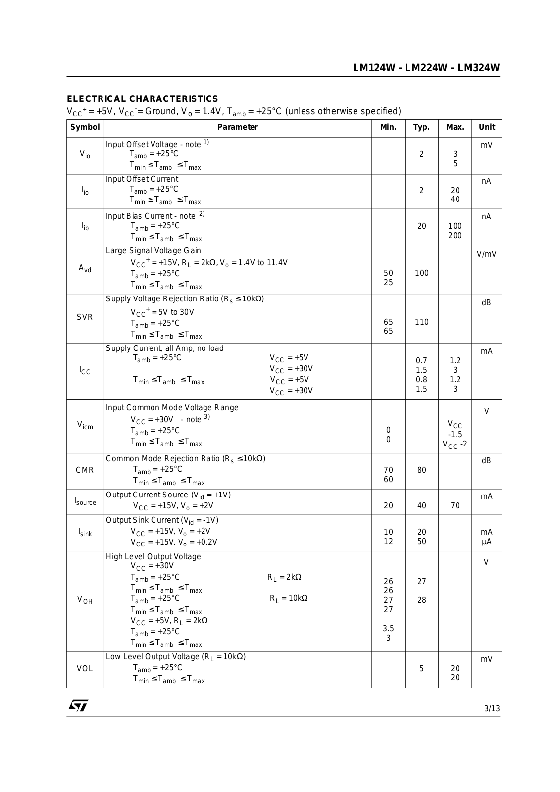
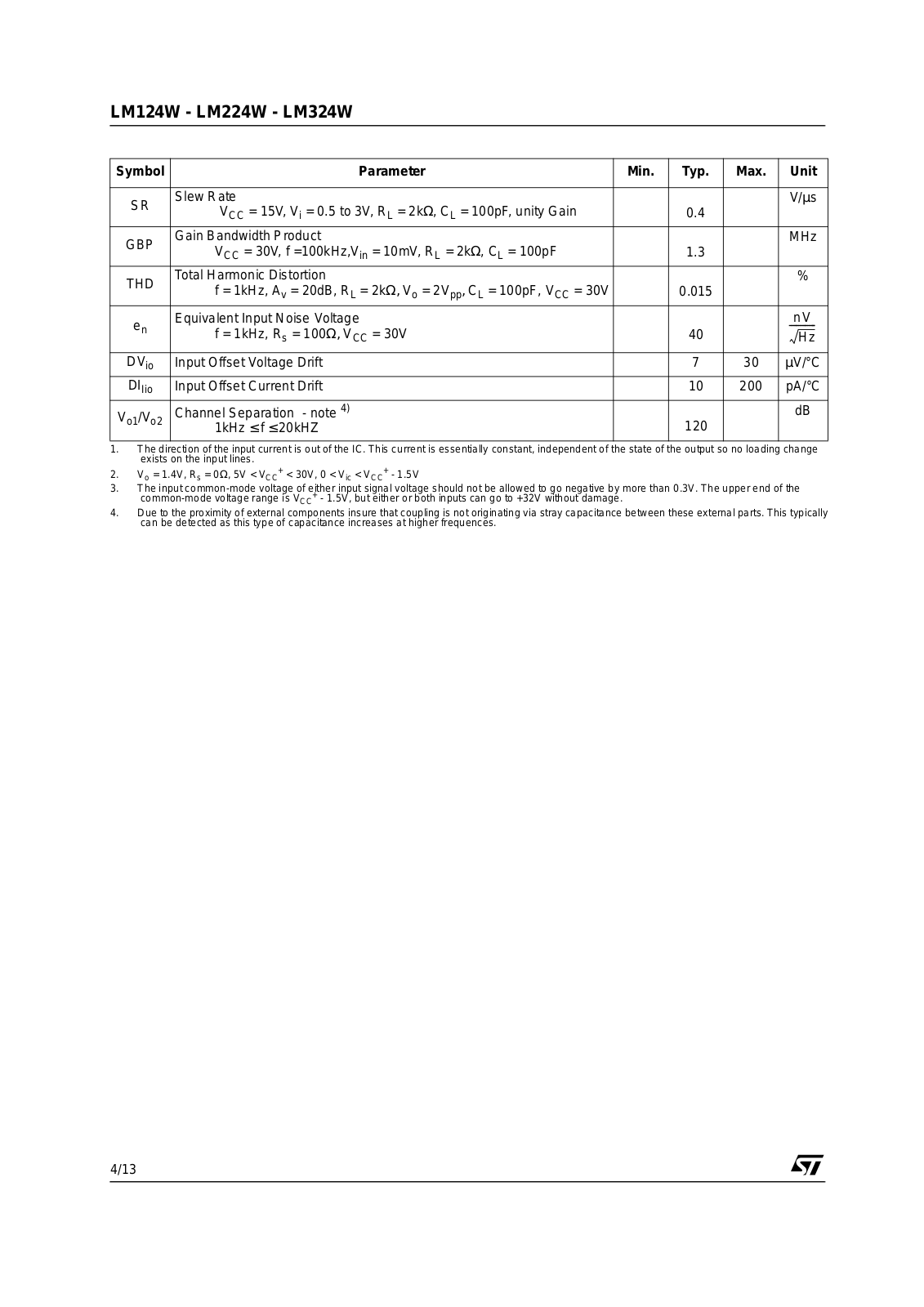
LM124
4
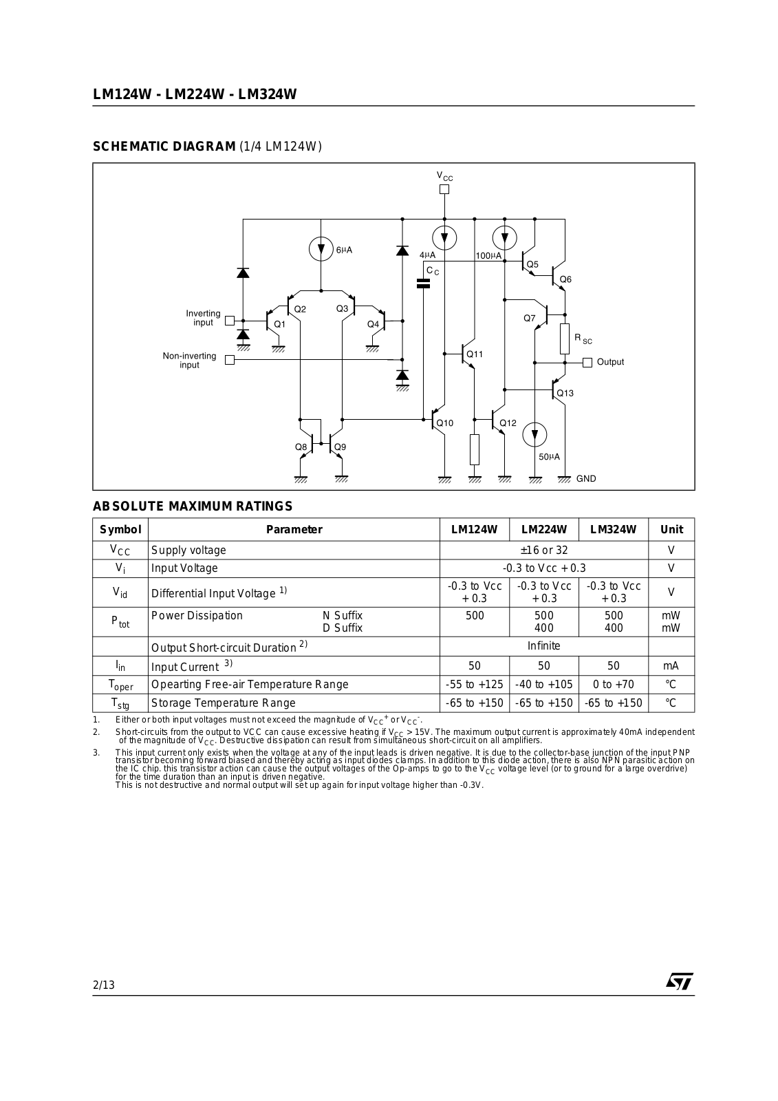
LM124W
2
LM134
LM135
LM137
LM138
LM139
LM146
2
LM148
LM158
2
LM158 A
LM158W
LM193
LM193A
LM201A
LM211
LM217
LM217L
LM217M
LM219
2
LM223
LM224
4
LM224A
LM224W
2
LM234
LM235
LM236
2
LM238
LM239
LM246
2
LM248
LM258
2
LM258 A
LM258W
LM2901
LM2901H
LM2902W
LM2903
LM2903H
LM2903W
LM2904
2
LM2904A
LM2904W
LM2904WH
LM293
LM293A
LM301A
LM311
LM317
LM317L
LM317M
Loading...
Loading...
Nothing found
LM124W
Operation Manual
13 pgs
623.1 Kb
0
User Manual
16 pgs
797.77 Kb
0
Table of contents
Loading...
ST LM124W, LM224W, LM324W Operation Manual
...
ST Operation Manual
Download
Specifications and Main Features
Frequently Asked Questions
User Manual
Download
Loading...
+
9
hidden pages
Unhide
You need points to download manuals.
1 point = 1 manual.
You can buy points or you can get point for every manual you upload.
Buy points
Upload your manuals
 Loading...