

现货库存、技术资料、百科信息、热点资讯,精彩尽在鼎好!
Low power quad operational amplifiers
Features
■ Wide gain bandwidth: 1.3 MHz
■ Input common-mode voltage range includes
ground
■ Large voltage gain: 100 dB
■ Very low supply current per amplifier: 375 µA
■ Low input bias current: 20 nA
■ Low input offset voltage: 5 mV max. (For more
accurate applications, use the equivalent parts
LM124A-LM224A-LM324A which feature 3 mV
max.)
■ Low input offset current: 2 nA
■ Wide power supply range:
– Single supply: +3 V to +30 V
– Dual supplies: ±1.5 V to ±15 V
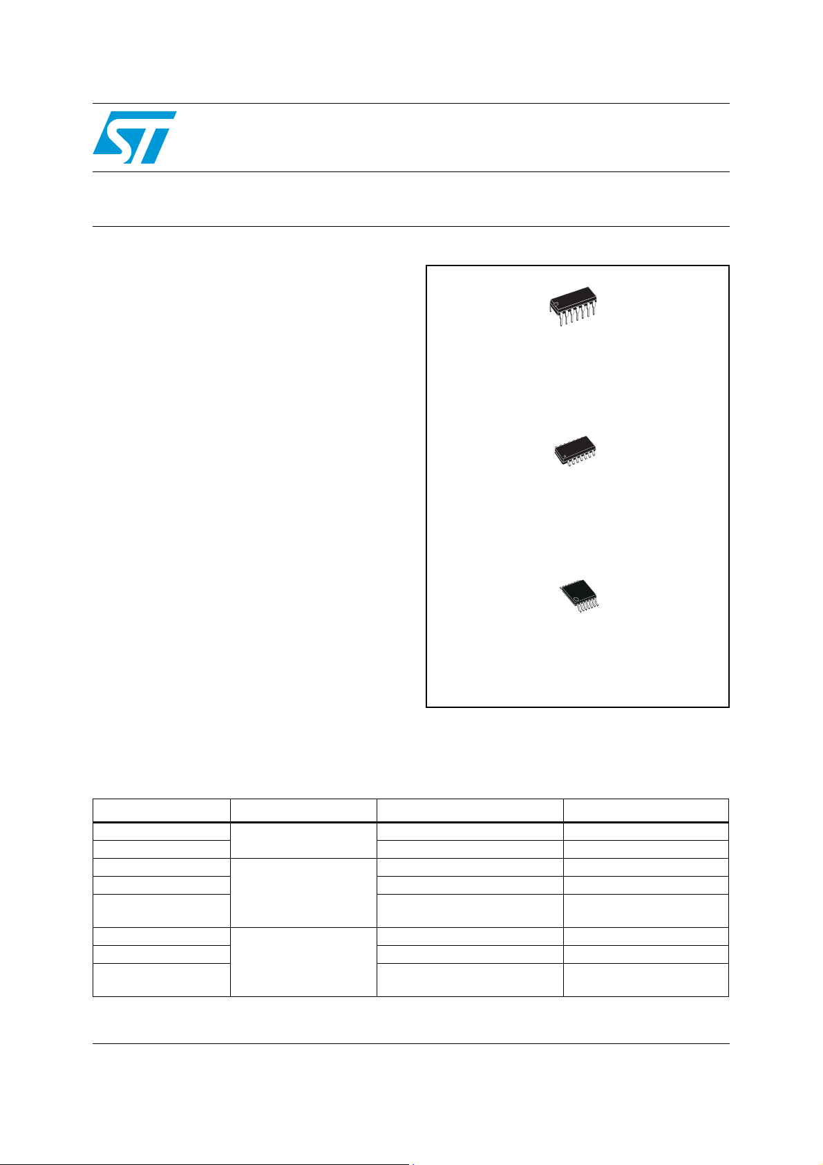
LM124-LM224-LM324
N
DIP14
(Plastic package)
D
SO-14
(Plastic micropackage)
Description
These circuits consist of four independent, high
gain, internally frequency compensated
operational amplifiers. Th ey o perate f rom a single
power supply over a wide range of voltages.
Operation from split power supplies is also
possible and the low po wer supply current drain is
independent of the magnitude of th e power supply
voltage.
(Thin shrink small outline package)
P
TSSOP-14
Order codes
Part number Tem perature range Package Packing
LM124N
LM124D/DT SO Tube or tape & reel
LM224N
LM224D/DT SO Tube or tape & reel
LM224PT
LM324N
LM324D/DT SO Tube or tape & reel
LM324PT
-55°C, +125°C
-40°C, +105°C
(Thin shrink outline package)
0°C, +70°C
(Thin shrink outline package)
DIP Tube
DIP Tube
TSSOP
DIP Tube
TSSOP
Tape & reel
Tape & reel
October 2006 Rev 5 1/19
www.st.com
19

Contents LM124-LM224-LM324
Contents
1 Pin & schematic diagram . . . . . . . . . . . . . . . . . . . . . . . . . . . . . . . . . . . . . 3
2 Absolute maximum ratings . . . . . . . . . . . . . . . . . . . . . . . . . . . . . . . . . . . 4
3 Electrical characteristics . . . . . . . . . . . . . . . . . . . . . . . . . . . . . . . . . . . . . 5
4 Typical single-supply applications . . . . . . . . . . . . . . . . . . . . . . . . . . . . 10
5 Macromodels . . . . . . . . . . . . . . . . . . . . . . . . . . . . . . . . . . . . . . . . . . . . . . 12
6 Package information . . . . . . . . . . . . . . . . . . . . . . . . . . . . . . . . . . . . . . . . 14
6.1 DIP14 package . . . . . . . . . . . . . . . . . . . . . . . . . . . . . . . . . . . . . . . . . . . . . 15
6.2 SO-14 package . . . . . . . . . . . . . . . . . . . . . . . . . . . . . . . . . . . . . . . . . . . . 16
6.3 TSSOP14 package . . . . . . . . . . . . . . . . . . . . . . . . . . . . . . . . . . . . . . . . . . 17
7 Revision history . . . . . . . . . . . . . . . . . . . . . . . . . . . . . . . . . . . . . . . . . . . 18
2/19
LM124-LM224-LM324 Pin & schematic diagram
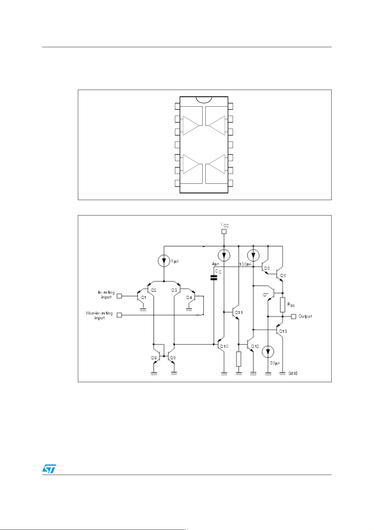
1 Pin & schematic diagram
Figure 1. Pin connections (top view)
Output 1
Inverting Input 1
Non-inverting Input 1
Non-inverting Input 2
Inverting Input 2
Output 2
1
2
-
+
3
+
V
4
CC
5
+
-
6
7
Figure 2. Schematic diagram (1/4 LM124)
Output 4
14
Inverting Input 4
13
-
+
+
-
Non-inverting Input 4
12
-
V
11
CC
10
Non-inverting Input 3
Inverting Input 3
9
Output 3
8
3/19
Absolute maximum ratings LM124-LM224-LM324
2 Absolute maximum ratings
Table 1. Absolute maximum ratings
Symbol Parameter LM124 LM224 LM324 Unit
V
V
Supply voltage ±16 or 32 V
CC
V
Input voltage 32 V
i
Differential input voltage
id
(1)
32 V
Pow er dissipation
P
tot
I
in
T
oper
T
stg
T
R
thja
R
thjc
ESD
N suffix
D suffix
Output short-circuit duration
Input current
(3)
(2)
500 500
400
Infinite
50 50 50 mA
Operating free-air temperature range -55 to +125 -40 to +105 0 to +70 °C
Storage temperature range -65 to +150 °C
Maximum junction temperature 150 °C
j
Thermal resistance junction to ambient
SO14
TSSOP14
DIP14
Thermal resistance junction to case
SO14
TSSOP14
DIP14
HBM: human body model
(5)
(6)
(4)
103
100
83
31
32
33
250
150
500
400
mW
°C/W
°C/W
VMM: machine model
CDM: charged device model 1500
+
1. Either or both input voltages must not exceed the magnitude of V
2. Short-circuits from the output to VCC can cause excessive heating if VCC > 15V. The maximum output
current is approximately 40 mA independent of the magnitude of V
from simultaneous short-circuits on all amplifiers.
3. This input current only exists when the voltage at any of the input leads is driven negative. It is due to the
collector-base junction of the input PNP transistor becoming forward biased and thereby acting as input
diode clamps. In addition to this diode action, there is also NPN parasitic action on the IC chip. This
transistor action can cause the output voltages of the op-amps to go to the V
for a large overdrive) for the time during which an input is driven negative.
This is not destructive and normal output is restored for input voltages above -0.3 V.
4. Short-circuits can cause excessive heating. Destructive dissipation can result from simultaneous shortcircuits on all amplifiers. These are typical values given for a single layer board (except for TSSOP, a twolayer board).
5. Human body model, 100 pF discharged through a 1.5 kΩ resistor into pin of device.
6. Machine model ESD, a 200 pF cap is charged to the specified voltage, then discharged directly into the IC
with no external series resistor (internal resistor < 5 Ω), into pin-to-pin of device.
CC
CC
-
or V
.
CC
. Destructive dissipation can result
voltage level (or to ground
CC
4/19
LM124-LM224-LM324 Electrical characteristics
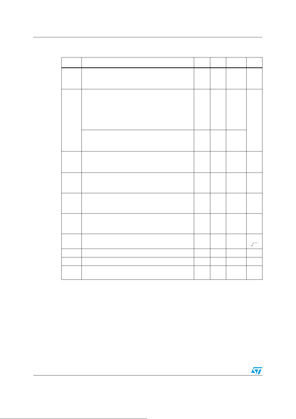
3 Electrical characteristics
Table 2. V
+
= +5 V, V
CC
-
= Ground, Vo = 1.4 V, T
CC
= +25° C (unless otherwise
amb
specified)
Symbol Parameter Min. Typ. Max. Unit
≤ T
≤ T
≤ T
≤ T
(3)
≤ T
≤ T
max
max
max
(2)
max
max
max
max
max
(1)
25
7
7
9
230
100
20 150
300
V/mV
≤ 10 kΩ)
s
5025100
6565110
≤ 10 kΩ)
s
70
0.7
1.5
0.8
1.5
0
0
80 dB
1.2
3
1.2
3
VCC -1.5
-2
V
CC
60
V
io
I
io
I
ib
A
vd
SVR
I
CC
V
icm
CMR
I
source
Input offset voltage
T
= +25° C
amb
LM124-LM224
LM324
T
≤ T
amb
≤ T
min
LM124-LM224
LM324
Input offset current
T
= +25° C
amb
T
≤ T
min
amb
Input bias current
T
= +25° C
amb
T
≤ T
min
amb
Large signal voltage gain
+
= +15 V, RL = 2 kΩ, Vo = 1.4 V to 11.4 V
V
CC
= +25° C
T
amb
T
≤ T
min
amb
Supply voltage rejection ratio (R
+
V
= 5 V to 30 V
CC
= +25° C
T
amb
T
≤ T
min
amb
Supply current, all Amp, no load
= +25° C
T
amb
VCC = +5 V
V
= +30 V
CC
≤ T
T
min
amb
≤ T
VCC = +5 V
V
= +30 V
CC
Input common mode voltage range
= +30 V
V
CC
T
= +25° C
amb
T
≤ T
min
amb
Common mode rejection ratio (R
T
= +25° C
amb
T
≤ T
min
amb
Output current source (Vid = +1 V)
= +15 V, Vo = +2 V 20 40 70 mA
V
CC
mV
nA
nA
dB
mA
V
5/19
Electrical characteristics LM124-LM224-LM324
Table 2. V
+
= +5 V, V
CC
-
= Ground, Vo = 1.4 V, T
CC
= +25° C (unless otherwise
amb
specified)
Symbol Parameter Min. Typ. Max. Unit
Output sink current (Vid = -1 V)
I
V
V
SR
sink
VCC = +15 V, Vo = +2 V
V
= +15 V, Vo = +0.2 V
CC
High level output voltage
= +30 V
V
CC
T
= +25° C, RL = 2 kΩ
amb
T
≤ T
≤ T
amb
max
= +25° C, RL = 10 kΩ
≤ T
≤ T
amb
max
= +25°C
≤ T
≤ T
amb
max
OH
min
T
amb
T
min
= +5 V, RL = 2 kΩ
V
CC
T
amb
T
min
Low level output voltage (RL = 10 kΩ)
= +25°C
OL
T
T
amb
min
≤ T
amb
≤ T
max
Slew rate
= 15 V, Vi = 0.5 to 3 V, RL = 2 kΩ, CL = 100 pF,
V
CC
unity gain
10
12
26
26
27
27
3.5
20
50
27
28
3
52020mV
0.4 V/µs
mA
µA
V
Gain bandwidth product
GBP
= 30 V, f = 100 kHz,V
V
CC
= 100 pF
C
L
= 10 mV, RL = 2 kΩ,
in
1.3 MHz
Total harmonic distortion
THD
f = 1 kHz, A
= 20 dB, RL = 2 kΩ, Vo = 2 Vpp,
v
0.015 %
CL = 100 pF, VCC = 30 V
Equivalent input noise voltage
e
n
f = 1 kHz, R
DV
DI
V
o1/Vo2
1. Vo = 1.4 V, Rs = 0 Ω, 5 V < V
2. The direction of the input current is out of the IC. This current is essentially constant, independent of the
3. The input common-mode voltage of either input signal voltage should not be allowed to go negative by
4. Due to the proximity of external components, ensure that stray capacitance between these external parts
Input offset voltage drift 7 30 µV/°C
io
Input offset current drift 10 200 pA/°C
io
Channel separation
1 kHz ≤ f ≤ 20 kHZ
state of the output so there is no change in the load on the input lines.
more than 0. V. The upper end of the common-mode voltage range is V
can go to +32 V without damage.
does not cause coupling. Typically, this can be detected because this type of capacitance increases at
higher frequencies.
= 100 Ω, VCC = 30 V
s
(4)
+
< 30 V, 0 < Vic < V
CC
CC
+
- 1.5 V
+
- 1.5 V, but either or both inputs
CC
40
120 dB
nV
----------- Hz
6/19
 Loading...