

查询LM123供应商
LM123/LM223
LM323
THREE-TERMINAL 3A-5V POSITIVE VOLTAGE REGULATORS
.OUTPUT CURRENT : 3A
.INTERNAL CURRENT AND THERMAL LIMI-
TING
.TYPICALOUPUT IMPEDANCE : 0.01Ω
.MINIMUMINPUT VOLTAGE: 7.5V
.POWER DISSIPATION : 30W
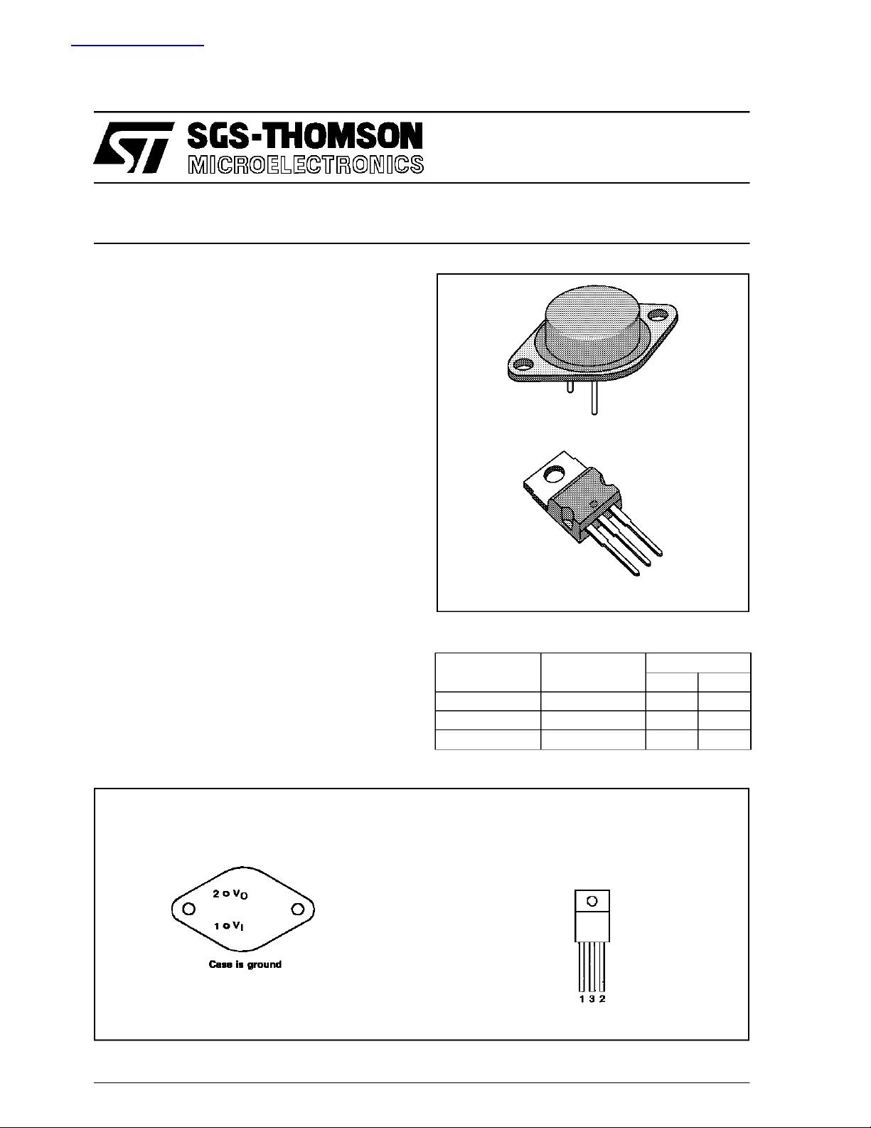
TO-3
DESCRI PTIO N
The LM123, LM223,LM323arethree-terminalpositive voltageregulators with a preset 5V output and
a load driving capability of 3A. New circuit design
and processing techniques areused to provide the
highoutputcurrent withoutsacrificing theregulation
characteristics of lower current devices.
The 3A regulator is virtually blowout proof.
Current limiting, power limiting and thermal shut-
down provide the same high level of reliability obtainedwith thesetechniques in theLM209, 1Aregulator.
An overallworstcasespecification for thecombined
effects of input voltage, load current, ambient temperature, and power dissipation ensure that the
LM123,LM223,LM323 will performsatisfactorily as
a system element.
ORDER CODES
Part Number Temperature
LM123 -55
LM223 -25
LM323 0
TO-220
Package
Range
o
C to 150oC •
o
C to 150oC •
o
C to 125oC ••
KT
PIN CONNEC T ION
(bot t om view)
March1993
TO-3
1 - Input
2 - Output
TO-220
(front view)
1 - Input
2 - Output
3 - GND
1/9
LM123-LM223-LM323
ABSOLU TE MAXIMU M RAT ING
Symbol Parameter Value Unit
V
Input Voltage 20 V
I
I
Output Current Internally Limited
O
P
Power Dissipation Internally Limited
tot
T
THERMA L CHA R ACTE R ISTI CS
Symbol Parameter Typ. Max. Unit
R
R
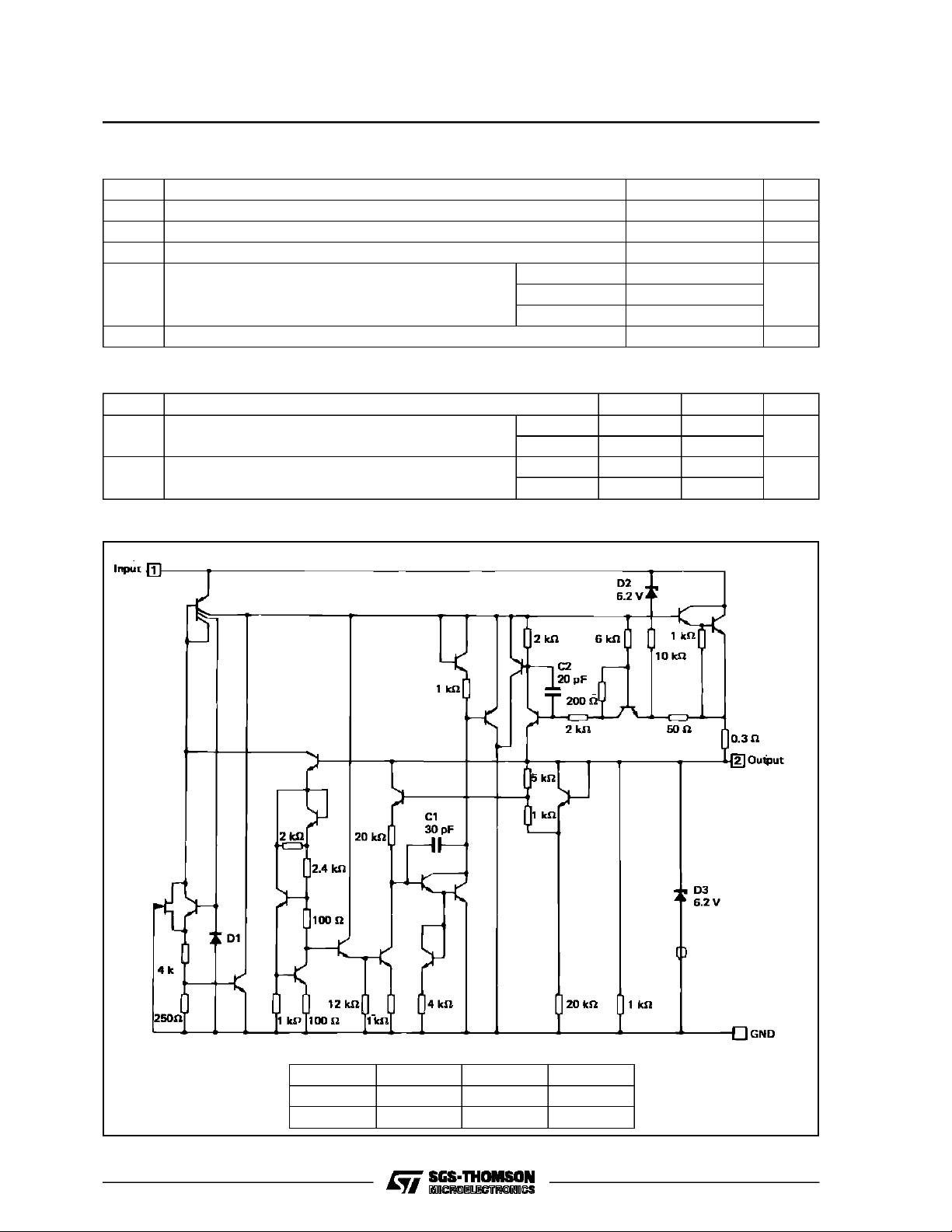
SCHEM ATIC D IA G RA M
Operating Junction Temperature Range LM123 -55 to 150
oper
LM223 -25 to 150
LM323 0 to 125
T
Storage Temperature Range -65 to 150
stg
Junction-case Thermal Resistance TO-3 2
thj-case
TO-220 3
Junction-ambient Thermal Resistance TO-3 35
thj-amb
TO-220 50
o
o
o
C
o
C
C/W
C/W
2/9
Case VI VO GND
TO-3 1 2 Case
TO-220 1 2 3
LM123-LM223-LM323
ELECTRIC AL CH A RAC TERI SI C S
LM123: -55oC<Tj<150oC
LM223: -25oC<Tj<150oC
LM323: 0oC<Tj<150oC
Symbol Parameter LM123/LM223 LM323 Unit
Min. Typ. Max. Min. Typ. Max.
V
Output Voltage Range (Note 2)
O
T
=25oC, VI= 7.5 V, IO=0
amb
V
Output Voltage Range (Note 2)
O
T
min
≤ Tj≤ T
max
,P≤P
max
7.5 V ≤ VI≤ 15 V, 0≤ IO≤ 3A
K
Line Regulation (Note 3)
VI
Tj=25oC, 7.5 V ≤ VI≤ 15V
K
Load Regulation (Note 3)
VO
Tj=25oC, VI= 7.5 V, 0 ≤ IO≤ 3A
I
Quiescent Current
IB
7.5 V ≤ V
V
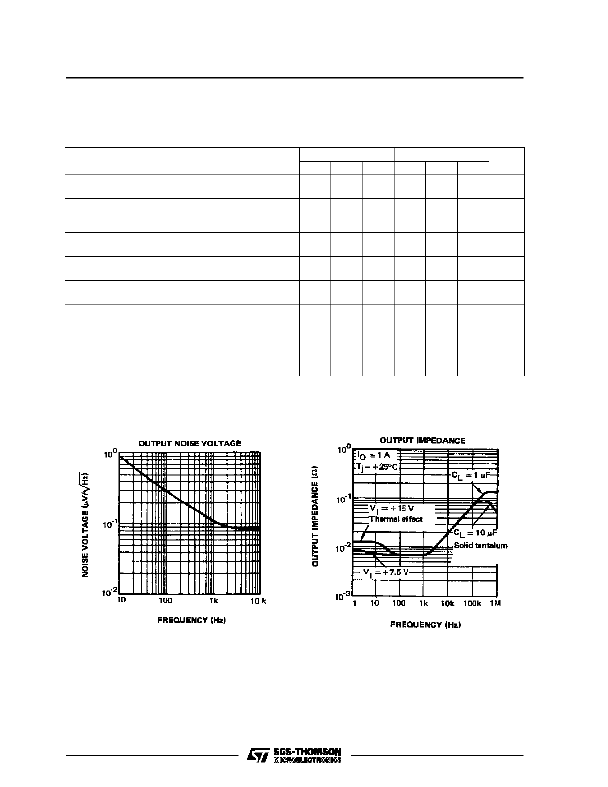
Output Noise Voltage
NO
T
amb
I
Short Circuit Current Limit (Tj=25oC)
OS
≤ 15 V, 0≤ IO≤ 3A
I
=25oC, 10 Hz ≤ f ≤ 100 KHz
VI=15V
VI= 7.5V
K
Notes : 1. Although power dissipation is internally limited, specifications apply only for P ≤ 30W.
Long Term Stability 35 35 mV
VH
2. Selected devices with tightened tolerance output voltage available.
3. Load and line regulation are specified at constant junction temperature. Pulse testing is required with a pulse width
≤ 1ms and a duty cycle ≤ 5%.
4.7 5 5.3 4.8 5 5.2 V
4.6 5.4 4.75 5.25 V
5 25 5 25 mV
25 100 25 100 mV
12 20 12 20 mA
40 40 µV
3
4.5
4
5
3
4.5
4
5
rms
A
A
3/9

LM123-LM223-LM323
4/9

LM123-LM223-LM323
TYPICAL APPLI CA TIONS
BASIC3A REGULATOR TRIMINGOUTPUT TO5V
C1= R equire d if regulator is distant from filter
capacito rs.
CL= R egulator is stable w ith no load capacitor into
resistive loads.
5/9

LM123-LM223-LM323
10A REGULA TO R WITH COMPLETE OVERLO AD PROTECTION
*
Selected for20mA currentfrom unregulated negative supply.
**
Solidtantalum.
A = LM101A, LM201A, LM301A.
ADJUSTABLE REGULATOR 0 – 10V/3A
A1 = LM 101 A, LM 201 A, LM 301 A.
C1 = 2µF optional - improves ripple rejection, noise and transient response.
6/9

TO-3 MECHANICAL DATA
LM123-LM223-LM323
DIM.
mm inch
MIN. TYP. MAX. MIN. TYP. MAX.
A 11.00 13.10 0.433 0.516
B 0.97 1.15 0.038 0.045
C 1.50 1.65 0.059 0.065
D 8.32 8.92 0.327 0.351
E 19.00 20.00 0.748 0.787
G 10.70 11.10 0.421 0.437
N 16.50 17.20 0.649 0.677
P 25.00 26.00 0.984 1.023
R 4.00 4.09 0.157 0.161
U 38.50 39.30 1.515 1.547
V 30.00 30.30 1.187 1.193
P
G
U
V
N
O
R
B
A
D
C
E
P003F
7/9

LM123-LM223-LM323
TO-220 MECHANICAL DATA
DIM.
mm inch
MIN. TYP. MAX. MIN. TYP. MAX.
A 4.40 4.60 0.173 0.181
C 1.23 1.32 0.048 0.051
D 2.40 2.72 0.094 0.107
D1 1.27 0.050
E 0.49 0.70 0.019 0.027
F 0.61 0.88 0.024 0.034
F1 1.14 1.70 0.044 0.067
F2 1.14 1.70 0.044 0.067
G 4.95 5.15 0.194 0.203
G1 2.4 2.7 0.094 0.106
H2 10.0 10.40 0.393 0.409
L2 16.4 0.645
L4 13.0 14.0 0.511 0.551
L5 2.65 2.95 0.104 0.116
L6 15.2 15.9 0.598 0.625
L7 6.2 6.6 0.244 0.260
L9 3.5 4.2 0.137 0.165
DIA. 3.75 3.85 0.147 0.151
E
A
L4
D
F2
F1
G1
H2
G
F
C
D1
L2
Dia.
L5
L7
L6
L9
P011C
8/9

LM123-LM223-LM323
Information furnished is believed to be accurate and reliable. However, SGS-THOMSON Microelectronics assumes no responsability for the
consequences of useof such information nor forany infringement of patents or other rights of third parties which may results from its use. No
license isgranted by implication or otherwise underany patent or patent rights of SGS-THOMSON Microelectronics. Specificationsmentioned
in this publication are subject to changewithout notice. This publication supersedes andreplaces all informationpreviously supplied.
SGS-THOMSON Microelectronicsproductsare not authorized foruse ascritical componentsin life support devices or systemswithout express
written approval of SGS-THOMSON Microelectonics.
1994 SGS-THOMSON Microelectronics- All RightsReserved
Australia - Brazil - France- Germany - Hong Kong - Italy - Japan - Korea - Malaysia- Malta - Morocco - The Netherlands-
Singapore - Spain - Sweden- Switzerland - Taiwan - Thailand - UnitedKingdom - U.S.A
SGS-THOMSON Microelectronics GROUP OF COMPANIES
9/9
 Loading...