

Features
■ Two independent comparators
■ Supply voltage: +5V to ±15V
■ Typically 80ns response time at ±15V
■ Minimum fan-out of 2 each side
■ Maximum input current of 1µa over operating
temperature range
■ Inputs and outputs can be isolated from system
ground
■ High common-mode slew rate
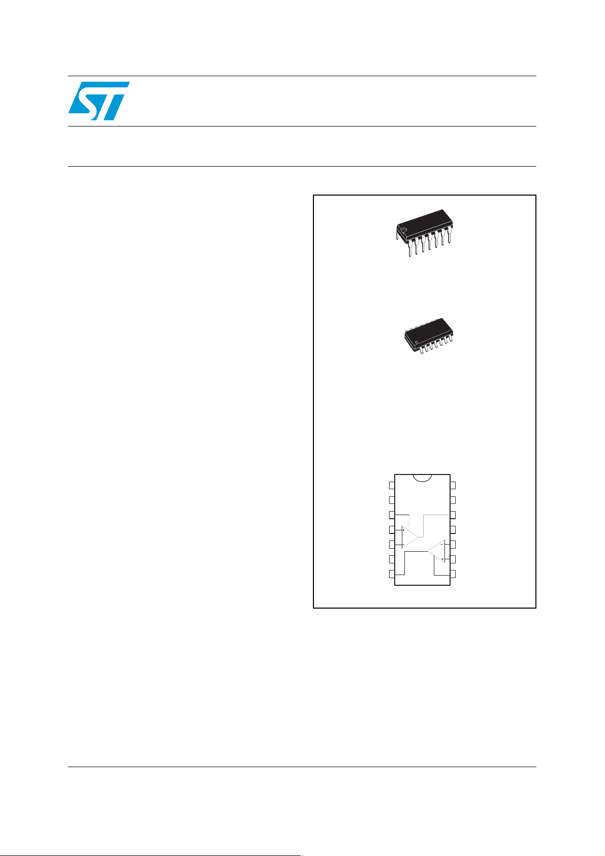
LM119-LM219-LM319
High speed dual comparators
DIP14
(Plastic package)
Description
These products are precision high speed dual
comparators designed to operate over a wide
range of supply voltages do wn to a single 5V logic
supply and ground. They feature low input
currents and high gains.
The open collector of the output stage makes it
compatible with TTL as well as capable of driving
lamps and relays at currents up to 25mA.
Although designed primarily for applications
requiring operation from digital logic supplies, the
comparators are fully specified f or po wer supplies
up to ±15V.
They feat ure faster response than LM111 at the
expense of higher current consumption. Howe v er,
the high speed, wide operating v oltag e ran ge and
low package count make the LM119/219/319
much more versatile.
N.C.
N.C.
Ground 1
Non-inverting input 1
Inverting input 1
V
CC
Output 2
SO-14
(Plastic micropackage)
Pin connections
(Top view)
1
2
3
4
5
-
6
7
14
13
12
11
10
9
8
N.C.
N.C.
Output 1
+
V
CC
Inverting input 2
Non-inverting input 2
Ground 2
January 2008 Rev 2 1/12
www.st.com
12
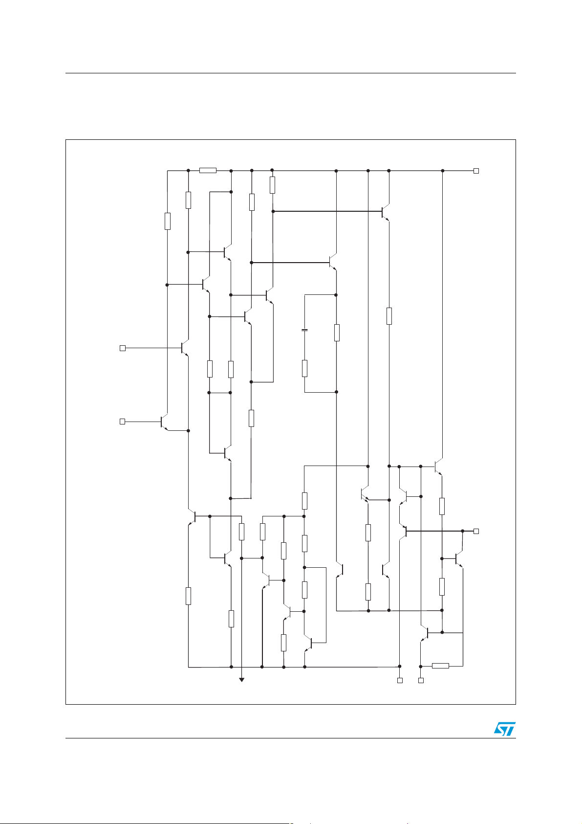
Schematic diagram LM119-LM219-LM319
1 Schematic diagram
Figure 1. Circuit schematics (1/2 LM119)
R1
R2
4kΩ
R3
4kΩ
3.5kΩ
R6
3kΩ
R7
3kΩ
Q9
+
V
CC
Inverting
Input
Non-inverting
Input
Q4
Q3
Q7
Q6
c1
18 Fμ
Q1
Q22
Q2
R4
3kΩ
600Ω
R25
R24
250Ω
Q6
Q21
R5
3kΩ
R23
4kΩ
Q20
R8
2kΩ
R22
60Ω
R20
3.6kΩ
R21
900Ω
Q19
R10
470kΩ
R9
18kΩ
Q18
-
+
R18
1.8kΩ
R19
250Ω
Q11
Q8
R11
13kΩ
600Ω
R13
R14
2kΩ
Q10
Q14
Q12
13kΩ
Q13
R12
Q17
R16
600Ω
R17
3Ω
Q15
R15
300Ω
Output
Q16
To other half
2/12
-
V
GND
CC
LM119-LM219-LM319 Absolute maximum ratings and operating conditions
2 Absolute maximum ratings and operating conditions
Table 1. Absolute maximum ratings (AMR)
Symbol Parameter Value Unit
-
- V
V
o
V
CC
V
CC
V
V
T
T
R
R
ESD
1. For supply voltages lower than ±15V the absolute maximum input voltage is equal to the supply voltage.
2. Short-circuits can cause excessive heating. Destructive dissipation can result from simultaneous shortcircuits on all amplifiers.
3. R
th
4. Human body model: 100pF discharged through a 1.5kΩ resistor between two pins of the device, done for
all couples of pin combinations with other pins floating.
5. Machine model: a 200pF cap is charged to the specified voltage, then discharged directly between two pins
of the device with no external series resistor (internal resistor < 5Ω), done for all couples of pin
combinations with other pins floating.
6. Charged device model: all pins and the package are charged together to the specified voltage and then
discharged directly to the ground through only one pin. This is done for all pins.
Table 2. Operating conditions
Output to negative supply voltage 36 V
CC
-
Negative supply voltage -25 V
+
Positive supply voltage 18 V
Differential input voltage ±5 V
id
i
Input voltage
(1)
±15 V
Output short-circuit to ground Infinite
Maximum junction temperature 150 °C
j
storage temperature range -65 to +150 °C
stg
Thermal resistance junction to ambient
thja
DIP14
SO-14
Thermal resistance junction to case
thjc
DIP14
SO-14
HBM: human body model
MM: machine model
(5)
CDM: charged device model
are typical values.
(4)
(6)
(2) (3)
80
105
(2) (3)
33
31
400
100
1500
°C/W
°C/W
V
Symbol Parameter Value Unit
V
Supply voltage 5 to ±15 V
CC
Operating free-air temperature range
T
oper
LM119
LM219
LM319
-55 to + 125
-40 to + 105
0 to + 70
°C
3/12
Electrical characteristics LM119-LM219-LM319
3 Electrical characteristics
Table 3. VCC = ±15V, Tamb = +25°C (unless otherwise specified)
LM119 - LM219 LM319
Symbol Parameter
Min. Typ. Max. Min Typ. Max.
V
I
I
A
Input offset voltage (Rs ≤ 5kΩ)
io
io
ib
vd
≤ T
≤ T
≤ T
amb
amb
amb
≤ T
≤ T
≤ T
max
(1)
max
(1)
max
T
min
Input offset current
T
min
Input bias current
T
min
Large signal voltage gain 10 40 8 40 V/mV
(1) (2)
0.7 4
7
30 75
100
150 500
1000
28
10
80 200
300
250 1000
1200
Positive supply current
+
I
CC
-
I
CC
V
CC
V
CC
= ±15V
+
= +5V, V
CC
-
= 0V
8
4.3
11.5 8
4.3
12.5
Negative supply current 3 4.5 3 5 mA
Input common mode voltage r a n ge
V
icm
VCC = ±15V
+
V
= +5V, V
CC
CC
-
= 0V
±121±13
±121±13
3
3
Low level output voltage
= 25mA
I
o
≤ -5mV
V
i
V
OL
Vi ≤ -10mV
≤ T
T
min
+
V
≥ +4.5V, V
CC
≤ -6mV
V
i
amb
≤ T
max
CC
-
= 0V, I
o(sink)
< 3.2mA
Vi ≤ -10mV
0.75
0.23
1.5
0.4
0.75
0.3
1.5
0.4
High level output current (Vo = +35V)
≥ 5mV
V
I
OH
t
res
1. These specifications apply for VCC = ±15V, unless otherwise stated.The offset voltage, offset current and bias current
specifications apply for any supply voltage from a single +5V up to ±15V supplies. The offset voltages and offset current
given are the maximum values required to drive the output down to 1V or up to +14V with a 1mA load current. Thus, these
parameters define an error band and take into account the worst case effects of voltage gain and input impedance.
2. At output switch point, Vo ≈ 1.4V, no load, with V
3. The response time specified is for a 100mV input step with 5mV overdrive.
i
V
≥ 10mV
i
≤ T
amb
≤ T
T
min
Response time
, Vi ≥ 5mV
max
(3)
80 80 ns
from 5V to ±15V and over the full input common-mode range.
CC
0.2
1
2
0.2 10
10
Unit
mV
nA
nA
mA
V
V
μA
4/12

LM119-LM219-LM319 Electrical characteristics
Figure 2. Input bias currents (LM119-219) Figure 3. Common mode limits (LM119-219)
Figure 4. Output saturation voltage (LM119-
Figure 5. Supply current (LM119-219)
219)
Figure 6. Supply current (LM119-219) Figure 7. Output limiting characteristics
(LM119-219)
5/12

Electrical characteristics LM119-LM219-LM319
Figure 8. Input bias currents (LM319) Figure 9. Common mode limits (LM319)
Figure 10. Output saturation volta ge (LM319) Figure 11. Supply current (LM319)
Figure 12. Transfer function Figure 13. Input characteristics
6/12

LM119-LM219-LM319 Electrical characteristics
Figure 14. Response time for various input
overdrives
Figure 16. Response time for various input
overdrives
Figure 15. Response time for various input
overdrives
Figure 17. Response time for various input
overdrives
7/12

Typical application diagrams LM119-LM219-LM319
4 Typical application diagrams
Figure 18. Relay driver
+28V
+5V
Inputs
Figure 19. Window detector
V
UT
V
I
V
LT
1/2
LM119
1/2
LM119
1/2
LM119
30V
500W
V
O
TTL output
= +5V for < <
V
O
=0for < or >
V
O
V
LT
V
V
I
V
V
I
UT
V
V
LT
I
UT
8/12

LM119-LM219-LM319 Package information
5 Package information
In order to meet environmental requ irements, ST offers these devices in ECOPACK®
packages. These packages have a lead-free second level interconnect. The category of
second level interconnect is marked on the package and on the inner box label, in
compliance with JEDEC Standard JESD97. The maximum ratings related t o soldering
conditions are also marked on the inner box label. ECOPACK is an ST trademark.
ECOPACK specifications are available at: www.st.com
5.1 DIP14 package information
Figure 20. DIP14 package mechanical drawing
.
Table 4. DIP14 package mechanical data
Dimensions
Ref.
Min. Typ. Max. Min. Typ. Max.
a1 0.51 0.020
B 1.39 1.65 0.055 0.065
b0.5 0.020
b1 0.25 0.010
D200.787
E8.5 0.335
e 2.54 0.100
e3 15.24 0.600
F 7.1 0.280
I 5.1 0.201
L3.3 0.130
Z 1.27 2.54 0.050 0.100
Millimeters Inches
9/12

Package information LM119-LM219-LM319
5.2 SO-14 package information
Figure 21. SO-14 package mechanical drawing
Table 5. SO-14 package mechanical data
Dimensions
Ref.
Min. Typ. Max. Min. Typ. Max.
A1.750.068
a1 0.1 0.2 0.003 0.007
a2 1.65 0.064
b 0.35 0.46 0.013 0.018
b1 0.19 0.25 0.007 0.010
C0.5 0.019
c1 45° (typ.)
D 8.55 8.75 0.336 0.344
E 5.8 6.2 0.228 0.244
e 1.27 0.050
e3 7.62 0.300
F 3.8 4.0 0.149 0.157
G 4.6 5.3 0.181 0.208
L 0.5 1.27 0.019 0.050
Millimeters Inches
M0.680.026
S 8° (max.)
10/12

LM119-LM219-LM319 Ordering information
6 Ordering information
Table 6. Order codes
Order code Temperature range Package Packaging Marking
LM119N
LM119D
LM119DT
LM219N
LM219D
LM219DT
LM319N
LM319D
LM319DT
-55°C to +125°C
-40°C to +105°C
0°C to +70°C
7 Revision history
Table 7. Document revision history
Date Revision Changes
5-Jul-2002 1 Initial release.
28-Jan-2007 2
DIP14 Tube LM119N
SO-14
DIP14 Tube LM219N
SO-14
DIP14 Tube LM319N
SO-14
Added ESD, R
(AMR).
Expanded orderable parts table, see Table 6: Order codes.
Updated document format.
parameters in Table 1: Absolute maximum ratings
thja
Tube or
Tape & reel
Tube or
Tape & reel
Tube or
Tape & reel
119
219
319
11/12

LM119-LM219-LM319
Please Read Carefully:
Information in this document is provided solely in connection with ST products. STMicroelectronics NV and its subsidiaries (“ST”) reserve the
right to make changes, corrections, modifications or improvements, to this document, and the products and services described herein at any
time, without notice.
All ST products are sold pursuant to ST’s terms and conditions of sale .
Purchasers are solely res ponsibl e fo r the c hoic e, se lecti on an d use o f the S T prod ucts and s ervi ces d escr ibed he rein , and ST as sumes no
liability whatsoever relati ng to the choice, selection or use of the ST products and services descri bed herein.
No license, express or implied, by estoppel or otherwise, to any intellectual property rights is granted under this document. If any part of this
document refers to any third pa rty p ro duc ts or se rv ices it sh all n ot be deem ed a lice ns e gr ant by ST fo r t he use of su ch thi r d party products
or services, or any intellectua l property c ontained the rein or consi dered as a warr anty coverin g the use in any manner whats oever of suc h
third party products or servi ces or any intellectual property contained therein.
UNLESS OTHERWISE SET FORTH IN ST’S TERMS AND CONDITIONS OF SALE ST DISCLAIMS ANY EXPRESS OR IMPLIED
WARRANTY WITH RESPECT TO THE USE AND/OR SALE OF ST PRODUCTS INCLUDING WITHOUT LIMITATION IMPLIED
WARRANTIES OF MERCHANTABILITY, FITNESS FOR A PARTICUL AR PURPOS E (AND THEIR EQUIVALE NTS UNDER THE LAWS
OF ANY JURISDICTION), OR INFRINGEMENT OF ANY PATENT, COPYRIGHT OR OTHER INTELLECTUAL PROPERTY RIGHT.
UNLESS EXPRESSLY APPROVED IN WRITING BY AN AUTHORIZED ST REPRESENTATIVE, ST PRODUCTS ARE NOT
RECOMMENDED, AUTHORIZED OR WARRANTED FOR USE IN MILITARY, AIR CRAFT, SPACE, LIFE SAVING, OR LIFE SUSTAINING
APPLICATIONS, NOR IN PRODUCTS OR SYSTEMS WHERE FAILURE OR MALFUNCTION MAY RESULT IN PERSONAL INJ URY,
DEATH, OR SEVERE PROPERTY OR ENVIRONMENTAL DAMAGE. ST PRODUCTS WHICH ARE NOT SPECIFIED AS "AUTOMOTIVE
GRADE" MAY ONLY BE USED IN AUTOMOTIVE APPLICATIONS AT USER’S OWN RISK.
Resale of ST products with provisions different from the statements and/or technical features set forth in this document shall immediately void
any warranty granted by ST fo r the ST pro duct or serv ice describe d herein and shall not cr eate or exten d in any manne r whatsoever , any
liability of ST.
ST and the ST logo are trademarks or registered trademarks of ST in various countries.
Information in this document su persedes and replaces all informa tion previously supplied.
The ST logo is a registered trademark of STMicroelectronics. All other names are the property of their respective owners.
© 2008 STMicroelectronics - All rights reserved
STMicroelectronics group of compan ie s
Australia - Belgium - Brazil - Canada - China - Czech Republic - Finland - France - Germany - Hong Kong - India - Israel - Ita ly - Japan -
Malaysia - Malta - Morocco - Singapore - Spain - Sweden - Switzerland - United Kingdom - United States of America
www.st.com
12/12
 Loading...