

ST LK112SM13TR, LK112SM14TR, LK112SM18TR, LK112SM19TR, LK112SM20TR User Manual
...
Low noise low drop voltage regulator with shutdown function
Features
■ Output current up to 200 mA
■ Low dropout voltage (500 mV max at
I
= 200 mA)
OUT
■ Very low quiescent current: 0.1 µA in OFF
mode and max 250 µA in ON mode at
I
= 0 mA
OUT
■ Low output noise: typ. 30 µV at I
and 10 Hz < f < 80 kHz
■ Wide range of output voltages
■ Internal current and thermal limit
■ V
■ Operative input voltage from:
tolerance ± 2% (at 25 °C)
OUT
V
+ 0.5 to 14 V (for V
OUT
OUT
or from 2.5 V to 14 V (for V
> 2 V)
OUT
Description
The LK112Sxx is a low dropout linear regulator
with a built in electronic switch. The internal
switch can be controlled by TTL or CMOS logic
levels. The device is ON state when the control
pin is pulled to a logic high level. An external
capacitor can be used connected to the noise
bypass pin to lower the output noise level to 30
OUT
< 2 V)
= 60 mA
LK112Sxx
SOT23-5L
µVrms. An internal PNP pass transistor is used to
achieve a low dropout voltage.
The LK112Sxx has a very low quiescent current
in ON MODE while in OFF MODE the Iq is
reduced down to 100 nA max. The internal
thermal shutdown circuitry limits the junction
temperature to below 150 °C. The load current is
internally monitored and the device will shutdown
in the presence of a short circuit or overcurrent
condition at the output.
Table 1. Device summary
Part numbers
LK112SXX13 LK112SXX24 LK112SXX36 LK112SXX45
LK112SXX14 LK112SXX26 LK112SXX37 LK112SXX46
LK112SXX18 LK112SXX28 LK112SXX38 LK112SXX47
LK112SXX19 LK112SXX29 LK112SXX39 LK112SXX48
LK112SXX20 LK112SXX31 LK112SXX41 LK112SXX49
LK112SXX21 LK112SXX33 LK112SXX42 LK112SXX50
LK112SXX22 LK112SXX34 LK112SXX43
LK112SXX23 LK112SXX35 LK112SXX44
July 2008 Rev 11 1/17
www.st.com
17

Contents LK112Sxx
Contents
1 Diagram . . . . . . . . . . . . . . . . . . . . . . . . . . . . . . . . . . . . . . . . . . . . . . . . . . . 3
2 Pin configuration . . . . . . . . . . . . . . . . . . . . . . . . . . . . . . . . . . . . . . . . . . . 4
3 Maximum ratings . . . . . . . . . . . . . . . . . . . . . . . . . . . . . . . . . . . . . . . . . . . . 5
4 Electrical characteristics . . . . . . . . . . . . . . . . . . . . . . . . . . . . . . . . . . . . . 6
5 Typical characteristics . . . . . . . . . . . . . . . . . . . . . . . . . . . . . . . . . . . . . . . 7
6 Package mechanical data . . . . . . . . . . . . . . . . . . . . . . . . . . . . . . . . . . . . 12
7 Order codes . . . . . . . . . . . . . . . . . . . . . . . . . . . . . . . . . . . . . . . . . . . . . . 15
8 Revision history . . . . . . . . . . . . . . . . . . . . . . . . . . . . . . . . . . . . . . . . . . . 16
2/17
LK112Sxx Diagram
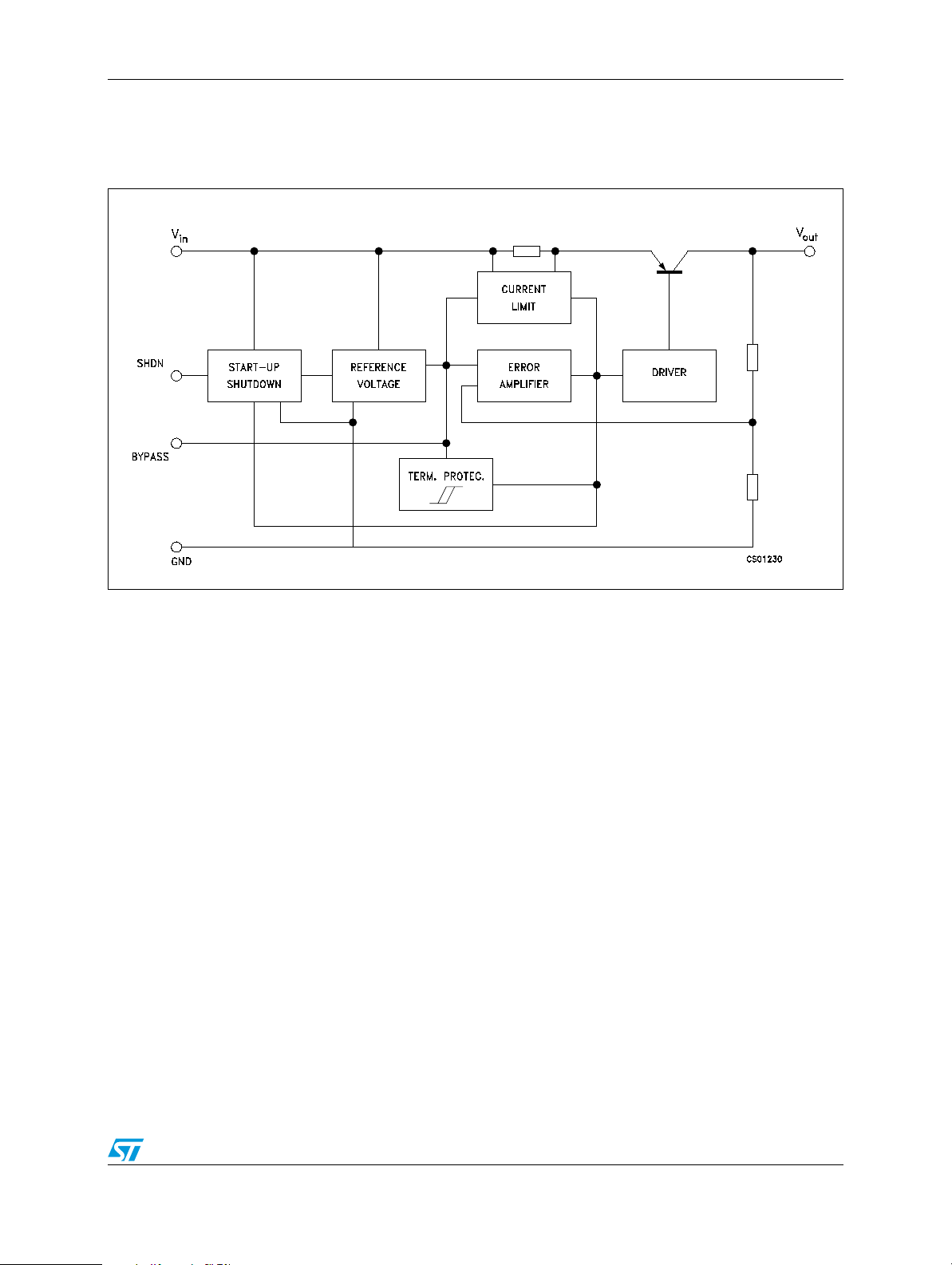
1 Diagram
Figure 1. Schematic diagram
3/17
Pin configuration LK112Sxx
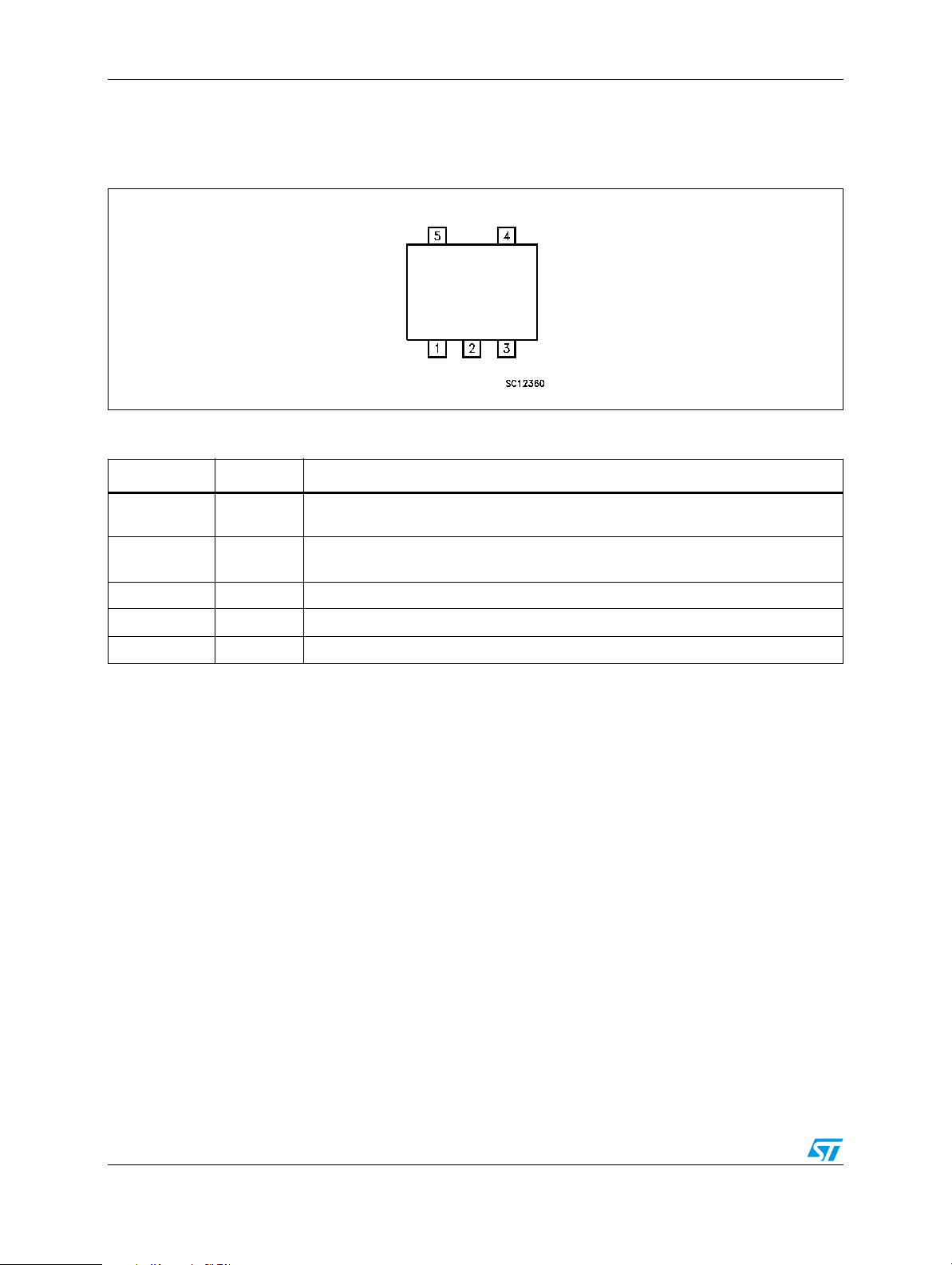
2 Pin configuration
Figure 2. Pin connection (top view)
Table 2. Pin description
Pin n° Symbol Note
1 SHDN
2GND
3 Bypass Bypass Pin: Bypass with 0.1 µF to improve the V
4 OUT Output port
5 IN Input port
Shutdown Input: Disables the regulator when is connected to GND or to positive
voltage less than 0.6 V
Ground Pin: Internally connected to the die attach flag to decrease the total thermal
resistance and increase the package ability to dissipate power.
thermal noise performances.
REF
4/17
LK112Sxx Maximum ratings
3 Maximum ratings
Table 3. Absolute maximum ratings
Symbol Parameter Value Unit
V
SHDN
T
T
V
I
I
O
STG
OP
DC input voltage 16 V
DC input voltage 16 V
Output current Internally limited
Storage temperature range -55 to 150 °C
Operating junction temperature range -40 to 125 °C
Table 4. Thermal data
Symbol Parameter SOT23-5L Unit
R
thJC
R
thJA
Thermal resistance junction-case 81 °C/W
Thermal resistance junction-ambient 255 °C/W
5/17
Electrical characteristics LK112Sxx
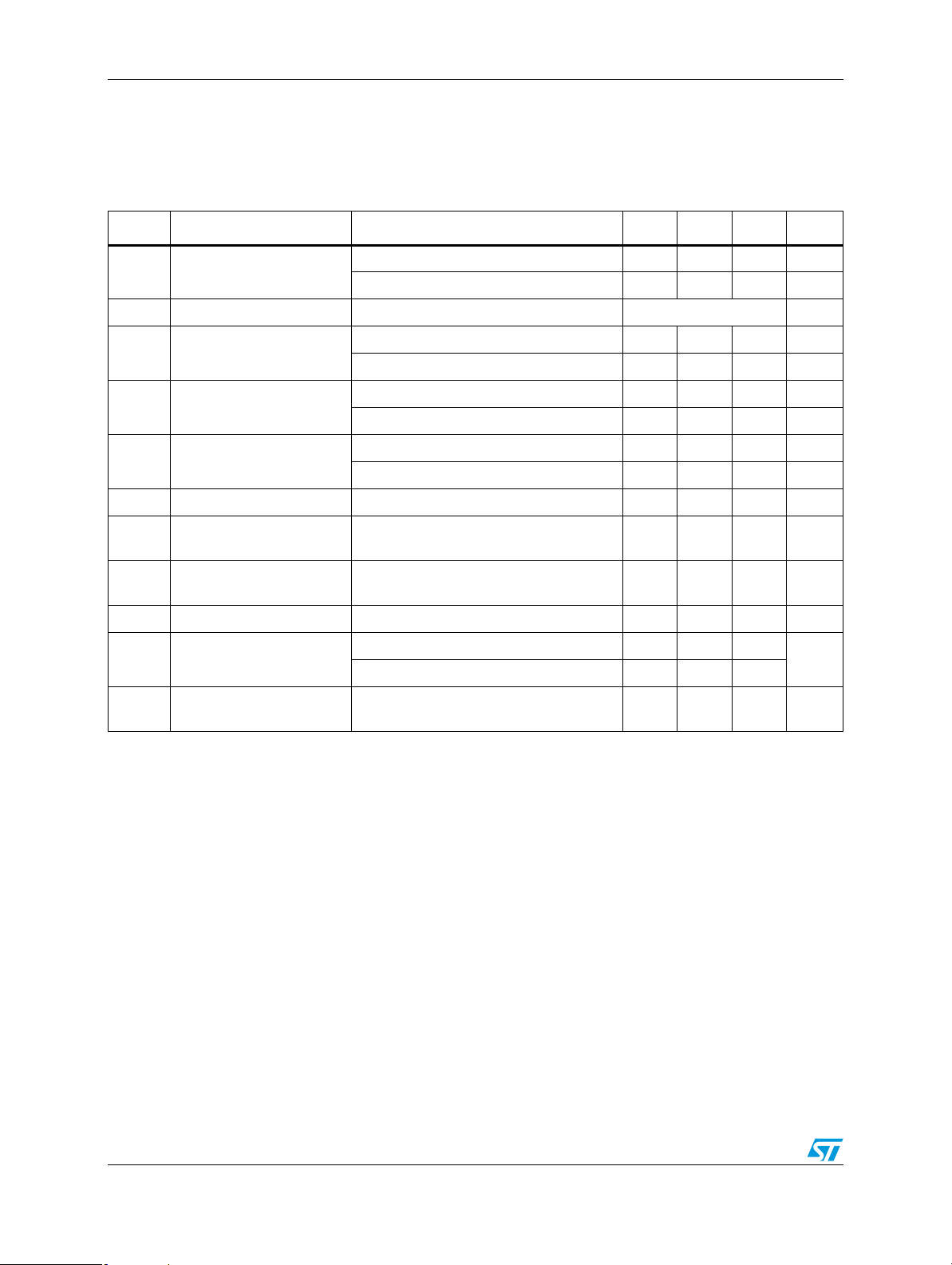
4 Electrical characteristics
Table 5. Electrical characteristics for LK112S (TJ = 25 °C, VIN=V
V
= 1.8 V, CI = 1 µF, CO = 2.2 µF, C
SHDN
BYPASS
= 0.1 µF unless otherwise specified)
OUT
+1 V
(1)
, I
OUT
= 0mA,
Symbol Parameter Test conditions Min. Typ. Max. Unit
I
Quiescent current
d
V
Output voltage IO = 30mA (see table)
O
ΔV
ΔV
Line regulation
O
Load regulation
O
V
Dropout voltage
d
Short circuit current 200 mA
I
SC
SVR Supply voltage rejection
eN Output noise voltage
I
SHDN
Shutdown input current V
ON MODE (except I
(2)
(2)
= 8V, V
I
BYP
OFF MODE, V
V
= VO+1V to VO+6V, VO ≤ 5.6V 0.7 20 mV
I
= VO+1V to VO+6V, VO > 5.6V 0.8 40 mV
V
I
I
= 1 to 60mA 15 30 mV
O
= 1 to 200mA 30 90 mV
I
O
I
= 60 mA
O
I
= 200 mA
O
= VO+1.5V, C
V
I
= 10µF, f = 400Hz, IO = 30mA
C
O
B= 10Hz to 80kHz, C
CO = 10µF, VI = VO+1.5V, IO = 60mA
= 1.8V, Output ON 12 35 µA
SHDN
)175250µA
SHDN
= 0V 0 0.1 µA
SHDN
0.17 0.24 V
0.35 0.5 V
= 0.1µF
= 0.1µF
BYP
55 dB
30 µVrms
Output ON 1.8
V
Shutdown input logic
SHDN
Output OFF 0.6
V
ΔVO/T
1. For version with output voltage less than 2V VIN=2.4V
2. Only for version with output voltage more than 2.1V
Output voltage
J
temperature coefficient
= 10mA 0.09 mV/°C
I
O
6/17
 Loading...