

3-axis ±2 g analog-output "piccolo" accelerometer
Features
■ Single voltage supply operation
■ ±2 g full-scale
■ 3 acceleration channels plus multiplexed
analog output
■ Ratiometric output voltage
■ Power-down mode
■ Embedded self-test
■ 10000 g high shock survivability
■ ECOPACK
(see Section 7)
Applications
■ Free-fall detection for data protection
■ Tilting applications
■ Gaming and virtual reality input devices
■ Antitheft systems and inertial navigation
®
RoHS and “Green” compliant
LIS352AR
MEMS motion sensor:
LGA-14
capacitors. The self-test capability allows the user
to check the functioning of the sensor in the final
application.
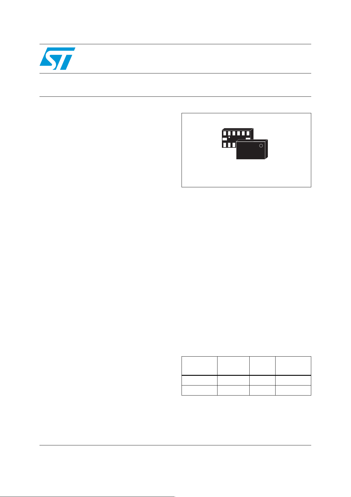
The device has three analog acceleration outputs,
plus an embedded multiplexer that allows for
redirection of the analog outputs onto a single pin
for operation with a single-channel A/D converter.
ST is already in the field with several hundred
million sensors which have received excellent
acceptance from the market in terms of quality,
reliability and performance
(3x5x0.9mm)
Description
The LIS352AR is a miniaturized low-power 3-axis
linear accelerometer belonging to the “piccolo”
family of ST motion sensors. It includes a sensing
element and an IC interface to provide an analog
signal to the external world.
The LIS352AR is provided in a plastic land grid
array (LGA) package.
Several years ago ST successfully pioneered the
usage of this package for accelerometers. Today,
ST has the widest manufacturing capability and
strongest expertise in the world for production of
sensors in plastic LGA packages.
The sensing element, capable of detecting the
acceleration, is manufactured using a dedicated
process developed by ST to produce motion
sensors and actuators in silicon.
The IC interface is manufactured using a CMOS
process that allows the design of a dedicated
circuit which is trimmed to better match the
sensing element characteristics.
Table 1. Device summary
Order code
LIS352AR -40 to +85 LGA-14 Tray
LIS352ARTR -40 to +85 LGA-14 Tape and reel
Temp.
range [°C]
Package Packing
The LIS352AR has a full-scale of ±2 g and is
capable of measuring accelerations over a
maximum bandwidth of 2.0 kHz. The device
bandwidth may be reduced by using external
February 2010 Doc ID 16933 Rev 1 1/15
www.st.com
15

Contents LIS352AR
Contents
1 Block diagram and pin description . . . . . . . . . . . . . . . . . . . . . . . . . . . . . 3
1.1 Pin connections and description . . . . . . . . . . . . . . . . . . . . . . . . . . . . . . . . 3
2 Mechanical and electrical specifications . . . . . . . . . . . . . . . . . . . . . . . . 5
2.1 Mechanical characteristics . . . . . . . . . . . . . . . . . . . . . . . . . . . . . . . . . . . . . 5
2.2 Electrical characteristics . . . . . . . . . . . . . . . . . . . . . . . . . . . . . . . . . . . . . . . 6
3 Absolute maximum ratings . . . . . . . . . . . . . . . . . . . . . . . . . . . . . . . . . . . 7
4 Terminology . . . . . . . . . . . . . . . . . . . . . . . . . . . . . . . . . . . . . . . . . . . . . . . . 8
4.1 Sensitivity . . . . . . . . . . . . . . . . . . . . . . . . . . . . . . . . . . . . . . . . . . . . . . . . . . 8
4.2 Zero-g level . . . . . . . . . . . . . . . . . . . . . . . . . . . . . . . . . . . . . . . . . . . . . . . . . 8
4.3 Self-test . . . . . . . . . . . . . . . . . . . . . . . . . . . . . . . . . . . . . . . . . . . . . . . . . . . 8
4.4 Output impedance . . . . . . . . . . . . . . . . . . . . . . . . . . . . . . . . . . . . . . . . . . . 8
5 Functionality . . . . . . . . . . . . . . . . . . . . . . . . . . . . . . . . . . . . . . . . . . . . . . . 9
5.1 Sensing element . . . . . . . . . . . . . . . . . . . . . . . . . . . . . . . . . . . . . . . . . . . . . 9
5.2 IC interface . . . . . . . . . . . . . . . . . . . . . . . . . . . . . . . . . . . . . . . . . . . . . . . . . 9
5.3 Factory calibration . . . . . . . . . . . . . . . . . . . . . . . . . . . . . . . . . . . . . . . . . . . 9
6 Application hints . . . . . . . . . . . . . . . . . . . . . . . . . . . . . . . . . . . . . . . . . . . 10
6.1 Soldering information . . . . . . . . . . . . . . . . . . . . . . . . . . . . . . . . . . . . . . . . 11
6.2 Output response vs. orientation . . . . . . . . . . . . . . . . . . . . . . . . . . . . . . . . 12
7 Package information . . . . . . . . . . . . . . . . . . . . . . . . . . . . . . . . . . . . . . . . 13
8 Revision history . . . . . . . . . . . . . . . . . . . . . . . . . . . . . . . . . . . . . . . . . . . 14
2/15 Doc ID 16933 Rev 1
LIS352AR Block diagram and pin description
1 Block diagram and pin description
Figure 1. Block diagram
a
SELF-TEST
X+
Y+
Z+
MUX
ZYX-
REFERENCE
CHARGE
AMPLIFIER
TRIMMING CIRCUIT
DEMUX
Routx
S/H
Routy
S/H
Routz
S/H
CLOCK
Aux_in
Voutx
Vouty
Voutz
Vout
MUX
S1 S0
AM06049v1
1.1 Pin connections and description
Figure 2. Pin connection
Z
X
Y
(TOP VIEW)
DIRECTIONS OF
DETECTABLE
ACCELERATIONS
1
Vdd
Aux_in
Vout
GND
Voutz
Vouty
Reserved
13
8
1
6
Voutx
(BOTTOM VIEW)
NC
Reserved
S0
S1
ST
PD
AM06050v1
Doc ID 16933 Rev 1 3/15

Block diagram and pin description LIS352AR
Table 2. Pin description
Pin # Pin name Function
1 NC Internally not connected
2 Reserved Connect to Vdd
3 S0 Mux selector 0 (connect to Vdd or to GND)
4 S1 Mux selector 1 (connect to Vdd or to GND)
5 ST Self-test (logic 0: normal mode; logic 1: self-test)
6 PD Power-down (logic 0: normal mode; logic 1: power-down mode)
7 Voutx Output voltage X channel
8 Vouty Output voltage Y channel
9 Voutz Output voltage Z channel
10 GND 0 V supply
11 Vout Multiplexer output
12 Aux_In Auxiliary input
13 Vdd Power supply
14 Reserved Connect to Vdd
4/15 Doc ID 16933 Rev 1

LIS352AR Mechanical and electrical specifications
2 Mechanical and electrical specifications
2.1 Mechanical characteristics
@ Vdd=3.3 V, T=25 °C unless otherwise noted
Table 3. Mechanical characteristics
Symbol Parameter Test condition Min. Typ.
Ar Acceleration range
(2)
(a)
.
(1)
±2 g
Max. Unit
So Sensitivity
SoDr
Sensitivity change vs.
temperature
Voff Zero-g level
OffDr
Zero-g level change
Vs temperature
NL Non linearity
CrossAx Cross-axis
Acceleration noise
An
density
Self-test output
Vt
voltage change
Fres
Sensing element
resonant frequency
(3)
(5)
(4)
(4)
(6),(7)
0.145*Vdd
–5%
0.145*Vdd
0.145*Vdd
+ 5%
Delta from +25 °C ±0.01 %/°C
T = 25 °C Vdd/2-6% Vdd/2 Vdd/2+6% V
Delta from +25 °C ±0.3 mg/°C
Best fit straight line ±0.5 % FS
±2 %
Vdd=3.3 V 100 µg/
T = 25 °C
Vdd=3.3 V
60 900 mV
X axis
T = 25 °C
Vdd=3.3 V
60 900 mV
Y axis
T = 25 °C
Vdd=3.3 V
60 900 mV
Z axis
All axes 2.0 kHz
(8)
V/g
Hz
Top
Operating
temperature range
Wh Product weight 30 mgram
1. Typical specifications are not guaranteed
2. Guaranteed by wafer level test and measurement of initial offset and sensitivity
3. Zero-g level and sensitivity are ratiometric to supply voltage
4. Guaranteed by design
a. The product is factory calibrated at 3.3 V. The operational power supply range is specified in Table 4. Since the
device is ratiometric, Voff, So and Vt parameters will vary with supply voltage.
Doc ID 16933 Rev 1 5/15
-40 +85 °C
 Loading...