

3-axis - ± 2g/± 8g smart digital output “piccolo” accelerometer
Feature
■ 2.16 V to 3.6 V supply voltage
■ 1.8 V compatible IOs
■ <1 mW power consumption
■ ± 2g/± 8g dynamically selectable full-scale
2
■ I
C/SPI digital output interface
■ Programmable multiple interrupt generator
■ Click and double click recognition
■ Embedded high pass filter
■ Embedded self test
■ 10000g high shock survivability
■ ECOPACK® RoHS and “Green” compliant
(see Section 9)
Description
The LIS302DL is an ultra compact low-power
three axes linear accelerometer. It includes a
sensing element and an IC interface able to
provide the measured acceleration to the external
world through I
The sensing element, capable of detecting the
acceleration, is manufactured using a dedicated
process developed by ST to produce inertial
sensors and actuators in silicon.
The IC interface is manufactured using a CMOS
process that allows to design a dedicated circuit
which is trimmed to better match the sensing
element characteristics.
2
C/SPI serial interface.
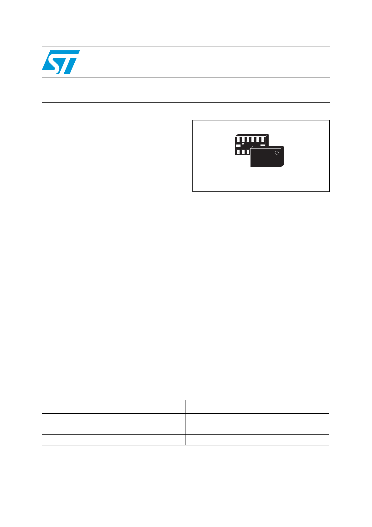
LIS302DL
MEMS motion sensor
LGA 14
The LIS302DL has dynamically user selectable
full scales of ± 2g/± 8g and it is capable of
measuring accelerations with an output data rate
of 100 Hz or 400 Hz.
A self-test capability allows the user to check the
functioning of the sensor in the final application.
The device may be configured to generate inertial
wake-up/free-fall interrupt signals when a
programmable acceleration threshold is crossed
at least in one of the three axes. Thresholds and
timing of interrupt generators are programmable
by the end user on the fly.
The LIS302DL is available in plastic Thin Land
Grid Array package (TLGA) and it is guaranteed
to operate over an extended temperature range
from -40 °C to +85 °C.
The LIS302DL belongs to a family of products
suitable for a variety of applications:
– Free-fall detection
– Motion activated functions
– Gaming and virtual reality input devices
– Vibration monitoring and compensation
(3x5x0.9mm)
Table 1. Device summary
Part number Temp range, ° CPackage Packing
LIS302DL -40 to +85 LGA Tray
LIS302DLTR -40 to +85 LGA Tape and reel ( 5000 pcs/reel )
LIS302DLTR8 -40 to +85 LGA Tape and reel ( 8000 pcs/reel )
October 2008 Rev 4 1/42
www.st.com
42

Contents LIS302DL
Contents
1 Block diagram and pin description . . . . . . . . . . . . . . . . . . . . . . . . . . . . . 8
1.1 Block diagram . . . . . . . . . . . . . . . . . . . . . . . . . . . . . . . . . . . . . . . . . . . . . . . 8
1.2 Pin description . . . . . . . . . . . . . . . . . . . . . . . . . . . . . . . . . . . . . . . . . . . . . . 8
2 Mechanical and electrical specifications . . . . . . . . . . . . . . . . . . . . . . . 10
2.1 Mechanical characteristics . . . . . . . . . . . . . . . . . . . . . . . . . . . . . . . . . . . . 10
2.2 Electrical characteristics . . . . . . . . . . . . . . . . . . . . . . . . . . . . . . . . . . . . . . 11
2.3 Communication interface characteristics . . . . . . . . . . . . . . . . . . . . . . . . . 12
2.3.1 SPI - Serial Peripheral Interface . . . . . . . . . . . . . . . . . . . . . . . . . . . . . . 12
2.3.2 I2C - inter IC control interface . . . . . . . . . . . . . . . . . . . . . . . . . . . . . . . . 13
2.4 Absolute maximum ratings . . . . . . . . . . . . . . . . . . . . . . . . . . . . . . . . . . . . 14
2.5 Terminology . . . . . . . . . . . . . . . . . . . . . . . . . . . . . . . . . . . . . . . . . . . . . . . 14
2.5.1 Sensitivity . . . . . . . . . . . . . . . . . . . . . . . . . . . . . . . . . . . . . . . . . . . . . . . . 14
2.5.2 Zero-g level . . . . . . . . . . . . . . . . . . . . . . . . . . . . . . . . . . . . . . . . . . . . . . 15
2.5.3 Self test . . . . . . . . . . . . . . . . . . . . . . . . . . . . . . . . . . . . . . . . . . . . . . . . . 15
2.5.4 Click and double click recognition . . . . . . . . . . . . . . . . . . . . . . . . . . . . . 15
3 Functionality . . . . . . . . . . . . . . . . . . . . . . . . . . . . . . . . . . . . . . . . . . . . . . 16
3.1 Sensing element . . . . . . . . . . . . . . . . . . . . . . . . . . . . . . . . . . . . . . . . . . . . 16
3.2 IC interface . . . . . . . . . . . . . . . . . . . . . . . . . . . . . . . . . . . . . . . . . . . . . . . . 16
3.3 Factory calibration . . . . . . . . . . . . . . . . . . . . . . . . . . . . . . . . . . . . . . . . . . 16
4 Application hints . . . . . . . . . . . . . . . . . . . . . . . . . . . . . . . . . . . . . . . . . . . 17
4.1 Soldering information . . . . . . . . . . . . . . . . . . . . . . . . . . . . . . . . . . . . . . . . 17
5 Digital interfaces . . . . . . . . . . . . . . . . . . . . . . . . . . . . . . . . . . . . . . . . . . . 18
5.1 I2C Serial Interface . . . . . . . . . . . . . . . . . . . . . . . . . . . . . . . . . . . . . . . . . . 18
5.1.1 I2C operation . . . . . . . . . . . . . . . . . . . . . . . . . . . . . . . . . . . . . . . . . . . . . 19
5.2 SPI bus interface . . . . . . . . . . . . . . . . . . . . . . . . . . . . . . . . . . . . . . . . . . . 20
5.2.1 SPI Read . . . . . . . . . . . . . . . . . . . . . . . . . . . . . . . . . . . . . . . . . . . . . . . . 22
5.2.2 SPI Write . . . . . . . . . . . . . . . . . . . . . . . . . . . . . . . . . . . . . . . . . . . . . . . . 22
5.2.3 SPI Read in 3-wires mode . . . . . . . . . . . . . . . . . . . . . . . . . . . . . . . . . . . 23
2/42

LIS302DL Contents
6 Register mapping . . . . . . . . . . . . . . . . . . . . . . . . . . . . . . . . . . . . . . . . . . 24
7 Register description . . . . . . . . . . . . . . . . . . . . . . . . . . . . . . . . . . . . . . . . 26
7.1 WHO_AM_I (0Fh) . . . . . . . . . . . . . . . . . . . . . . . . . . . . . . . . . . . . . . . . . . . 26
7.2 CTRL_REG1 (20h) . . . . . . . . . . . . . . . . . . . . . . . . . . . . . . . . . . . . . . . . . . 26
7.3 CTRL_REG2 (21h) . . . . . . . . . . . . . . . . . . . . . . . . . . . . . . . . . . . . . . . . . . 27
7.4 CTRL_REG3 [Interrupt CTRL register] (22h) . . . . . . . . . . . . . . . . . . . . . . 28
7.5 HP_FILTER_RESET (23h) . . . . . . . . . . . . . . . . . . . . . . . . . . . . . . . . . . . . 28
7.6 STATUS_REG (27h) . . . . . . . . . . . . . . . . . . . . . . . . . . . . . . . . . . . . . . . . . 29
7.7 OUT_X (29h) . . . . . . . . . . . . . . . . . . . . . . . . . . . . . . . . . . . . . . . . . . . . . . 29
7.8 OUT_Y (2Bh) . . . . . . . . . . . . . . . . . . . . . . . . . . . . . . . . . . . . . . . . . . . . . . 29
7.9 OUT_Z (2Dh) . . . . . . . . . . . . . . . . . . . . . . . . . . . . . . . . . . . . . . . . . . . . . . 30
7.10 FF_WU_CFG_1 (30h) . . . . . . . . . . . . . . . . . . . . . . . . . . . . . . . . . . . . . . . 30
7.11 FF_WU_SRC_1 (31h) . . . . . . . . . . . . . . . . . . . . . . . . . . . . . . . . . . . . . . . 31
7.12 FF_WU_THS_1 (32h) . . . . . . . . . . . . . . . . . . . . . . . . . . . . . . . . . . . . . . . 31
7.13 FF_WU_DURATION_1 (33h) . . . . . . . . . . . . . . . . . . . . . . . . . . . . . . . . . . 32
7.14 FF_WU_CFG_2 (34h) . . . . . . . . . . . . . . . . . . . . . . . . . . . . . . . . . . . . . . . 32
7.15 FF_WU_SRC_2 (35h) . . . . . . . . . . . . . . . . . . . . . . . . . . . . . . . . . . . . . . . 33
7.16 FF_WU_THS_2 (36h) . . . . . . . . . . . . . . . . . . . . . . . . . . . . . . . . . . . . . . . 33
7.17 FF_WU_DURATION_2 (37h) . . . . . . . . . . . . . . . . . . . . . . . . . . . . . . . . . . 33
7.18 CLICK_CFG (38h) . . . . . . . . . . . . . . . . . . . . . . . . . . . . . . . . . . . . . . . . . . 34
7.19 CLICK_SRC (39h) . . . . . . . . . . . . . . . . . . . . . . . . . . . . . . . . . . . . . . . . . . 34
7.20 CLICK_THSY_X (3Bh) . . . . . . . . . . . . . . . . . . . . . . . . . . . . . . . . . . . . . . . 35
7.21 CLICK_THSZ (3Ch) . . . . . . . . . . . . . . . . . . . . . . . . . . . . . . . . . . . . . . . . . 35
7.22 CLICK_TimeLimit (3Dh) . . . . . . . . . . . . . . . . . . . . . . . . . . . . . . . . . . . . . . 35
7.23 CLICK_Latency (3Eh) . . . . . . . . . . . . . . . . . . . . . . . . . . . . . . . . . . . . . . . 36
7.24 CLICK_Window (3Fh) . . . . . . . . . . . . . . . . . . . . . . . . . . . . . . . . . . . . . . . 36
8 Typical performance characteristics . . . . . . . . . . . . . . . . . . . . . . . . . . . 37
8.1 Mechanical characteristics at 25°C . . . . . . . . . . . . . . . . . . . . . . . . . . . . . 37
8.2 Mechanical characteristics derived from measurement in the -40°C to +85°C
temperature range . . . . . . . . . . . . . . . . . . . . . . . . . . . . . . . . . . . . . . . . . . 38
8.3 Electro-mechanical characteristics at 25°C . . . . . . . . . . . . . . . . . . . . . . . 39
3/42

Contents LIS302DL
9 Package information . . . . . . . . . . . . . . . . . . . . . . . . . . . . . . . . . . . . . . . . 40
10 Revision history . . . . . . . . . . . . . . . . . . . . . . . . . . . . . . . . . . . . . . . . . . . 41
4/42

LIS302DL List of tables
List of tables
Table 1. Device summary . . . . . . . . . . . . . . . . . . . . . . . . . . . . . . . . . . . . . . . . . . . . . . . . . . . . . . . . . . 1
Table 2. Pin description . . . . . . . . . . . . . . . . . . . . . . . . . . . . . . . . . . . . . . . . . . . . . . . . . . . . . . . . . . . 9
Table 3. Mechanical characteristics
(All the parameters are specified @ Vdd=2.5V, T = 25°C unless otherwise noted) . . . . . . 10
Table 4. Electrical characteristics
(All the parameters are specified @ Vdd=2.5V, T= 25°C unless otherwise noted) . . . . . . 11
Table 5. SPI slave timing values. . . . . . . . . . . . . . . . . . . . . . . . . . . . . . . . . . . . . . . . . . . . . . . . . . . . 12
Table 6. I2C slave timing values . . . . . . . . . . . . . . . . . . . . . . . . . . . . . . . . . . . . . . . . . . . . . . . . . . . . 13
Table 7. Absolute maximum ratings . . . . . . . . . . . . . . . . . . . . . . . . . . . . . . . . . . . . . . . . . . . . . . . . . 14
Table 8. Serial interface pin description . . . . . . . . . . . . . . . . . . . . . . . . . . . . . . . . . . . . . . . . . . . . . . 18
Table 9. Serial interface pin description . . . . . . . . . . . . . . . . . . . . . . . . . . . . . . . . . . . . . . . . . . . . . . 18
Table 10. SAD+Read/Write patterns . . . . . . . . . . . . . . . . . . . . . . . . . . . . . . . . . . . . . . . . . . . . . . . . . 19
Table 11. Transfer when master is writing one byte to slave . . . . . . . . . . . . . . . . . . . . . . . . . . . . . . . 19
Table 12. Transfer when master is writing multiple bytes to slave . . . . . . . . . . . . . . . . . . . . . . . . . . . 19
Table 13. Transfer when Master is receiving (reading) one byte of data from slave . . . . . . . . . . . . . 20
Table 14. ransfer when master is receiving (reading). . . . . . . . . . . . . . . . . . . . . . . . . . . . . . . . . . . . . 20
Table 15. Multiple bytes of data from slave . . . . . . . . . . . . . . . . . . . . . . . . . . . . . . . . . . . . . . . . . . . . 20
Table 16. Register address map. . . . . . . . . . . . . . . . . . . . . . . . . . . . . . . . . . . . . . . . . . . . . . . . . . . . . 24
Table 17. WHO_AM_I (0Fh) register . . . . . . . . . . . . . . . . . . . . . . . . . . . . . . . . . . . . . . . . . . . . . . . . . 26
Table 18. CTRL_REG1 (20h) register . . . . . . . . . . . . . . . . . . . . . . . . . . . . . . . . . . . . . . . . . . . . . . . . 26
Table 19. CTRL_REG1 (20h) register description . . . . . . . . . . . . . . . . . . . . . . . . . . . . . . . . . . . . . . . 26
Table 20. CTRL_REG2 (21h) register . . . . . . . . . . . . . . . . . . . . . . . . . . . . . . . . . . . . . . . . . . . . . . . . 27
Table 21. CTRL_REG2 (21h) register description . . . . . . . . . . . . . . . . . . . . . . . . . . . . . . . . . . . . . . . 27
Table 22. High pass filter cut-off frequency configuration. . . . . . . . . . . . . . . . . . . . . . . . . . . . . . . . . . 28
Table 23. CTRL_REG3 (22h) register . . . . . . . . . . . . . . . . . . . . . . . . . . . . . . . . . . . . . . . . . . . . . . . . 28
Table 24. CTRL_REG3 (22h) register description . . . . . . . . . . . . . . . . . . . . . . . . . . . . . . . . . . . . . . . 28
Table 25. CTRL_REG3 (22h) truth table . . . . . . . . . . . . . . . . . . . . . . . . . . . . . . . . . . . . . . . . . . . . . . 28
Table 26. STATUS_REG (27h) register . . . . . . . . . . . . . . . . . . . . . . . . . . . . . . . . . . . . . . . . . . . . . . . 29
Table 27. STATUS_REG (27h) register desription . . . . . . . . . . . . . . . . . . . . . . . . . . . . . . . . . . . . . . . 29
Table 28. OUT_X (29h) register . . . . . . . . . . . . . . . . . . . . . . . . . . . . . . . . . . . . . . . . . . . . . . . . . . . . . 29
Table 29. OUT_Y (2Bh) register description. . . . . . . . . . . . . . . . . . . . . . . . . . . . . . . . . . . . . . . . . . . . 29
Table 30. OUT_Z (2Dh) register . . . . . . . . . . . . . . . . . . . . . . . . . . . . . . . . . . . . . . . . . . . . . . . . . . . . . 30
Table 31. FF_WW_CFG_1 (30h) register. . . . . . . . . . . . . . . . . . . . . . . . . . . . . . . . . . . . . . . . . . . . . . 30
Table 32. FF_WW_CFG_1(30h) register description . . . . . . . . . . . . . . . . . . . . . . . . . . . . . . . . . . . . . 30
Table 33. FF_WU_SRC_1 (31h) register . . . . . . . . . . . . . . . . . . . . . . . . . . . . . . . . . . . . . . . . . . . . . . 31
Table 34. FF_WU_SRC_1 (31h) register description . . . . . . . . . . . . . . . . . . . . . . . . . . . . . . . . . . . . . 31
Table 35. FF_WU_THS_1 (32h) register . . . . . . . . . . . . . . . . . . . . . . . . . . . . . . . . . . . . . . . . . . . . . . 31
Table 36. FF_WU_THS_1 (32h) register description . . . . . . . . . . . . . . . . . . . . . . . . . . . . . . . . . . . . . 31
Table 37. FF_WU_DURATION_1 (33h) register . . . . . . . . . . . . . . . . . . . . . . . . . . . . . . . . . . . . . . . . 32
Table 38. FF_WU_DURATION_1 (33h) register description . . . . . . . . . . . . . . . . . . . . . . . . . . . . . . . 32
Table 39. FF_WU_CFG_2 (34h) register . . . . . . . . . . . . . . . . . . . . . . . . . . . . . . . . . . . . . . . . . . . . . . 32
Table 40. FF_WU_CFG_2 (34h) register description . . . . . . . . . . . . . . . . . . . . . . . . . . . . . . . . . . . . . 32
Table 41. FF_WU_SRC_2 (35h) register . . . . . . . . . . . . . . . . . . . . . . . . . . . . . . . . . . . . . . . . . . . . . . 33
Table 42. FF_WU_SRC_2 (35h) register description . . . . . . . . . . . . . . . . . . . . . . . . . . . . . . . . . . . . . 33
Table 43. FF_WU_THS_2 (36h) register . . . . . . . . . . . . . . . . . . . . . . . . . . . . . . . . . . . . . . . . . . . . . . 33
Table 44. FF_WU_THS_2 (36h) register description . . . . . . . . . . . . . . . . . . . . . . . . . . . . . . . . . . . . . 33
Table 45. FF_WU_DURATION_2 (37h) register . . . . . . . . . . . . . . . . . . . . . . . . . . . . . . . . . . . . . . . . 33
Table 46. FF_WU_DURATION_2 (37h) register description . . . . . . . . . . . . . . . . . . . . . . . . . . . . . . . 34
5/42

List of tables LIS302DL
Table 47. CLICK_CFG (38h) register . . . . . . . . . . . . . . . . . . . . . . . . . . . . . . . . . . . . . . . . . . . . . . . . . 34
Table 48. CLICK_CFG (38h) register description. . . . . . . . . . . . . . . . . . . . . . . . . . . . . . . . . . . . . . . . 34
Table 49. CLICK_CFG (38h) truth table . . . . . . . . . . . . . . . . . . . . . . . . . . . . . . . . . . . . . . . . . . . . . . . 34
Table 50. CLICK_SRC (39h) register . . . . . . . . . . . . . . . . . . . . . . . . . . . . . . . . . . . . . . . . . . . . . . . . . 34
Table 51. CLICK_SRC (39h) register description. . . . . . . . . . . . . . . . . . . . . . . . . . . . . . . . . . . . . . . . 35
Table 52. CLICK_THSY_X (3Bh) register . . . . . . . . . . . . . . . . . . . . . . . . . . . . . . . . . . . . . . . . . . . . . 35
Table 53. CLICK_THSY_X (3Bh) register description . . . . . . . . . . . . . . . . . . . . . . . . . . . . . . . . . . . . 35
Table 54. CLICK_THSZ (3Ch) register . . . . . . . . . . . . . . . . . . . . . . . . . . . . . . . . . . . . . . . . . . . . . . . . 35
Table 55. CLICK_THSZ (3Ch) register description. . . . . . . . . . . . . . . . . . . . . . . . . . . . . . . . . . . . . . . 35
Table 56. CLICK_TimeLimit (3Dh) register. . . . . . . . . . . . . . . . . . . . . . . . . . . . . . . . . . . . . . . . . . . . . 35
Table 57. CLICK_Latency (3Eh) register . . . . . . . . . . . . . . . . . . . . . . . . . . . . . . . . . . . . . . . . . . . . . . 36
Table 58. CLICK_Window (3Fh) register . . . . . . . . . . . . . . . . . . . . . . . . . . . . . . . . . . . . . . . . . . . . . . 36
Table 59. Document revision history . . . . . . . . . . . . . . . . . . . . . . . . . . . . . . . . . . . . . . . . . . . . . . . . . 41
6/42

LIS302DL List of figures
List of figures
Figure 1. Block diagram . . . . . . . . . . . . . . . . . . . . . . . . . . . . . . . . . . . . . . . . . . . . . . . . . . . . . . . . . . . . 7
Figure 2. Pin connection . . . . . . . . . . . . . . . . . . . . . . . . . . . . . . . . . . . . . . . . . . . . . . . . . . . . . . . . . . . 7
Figure 3. SPI slave timing diagram (2). . . . . . . . . . . . . . . . . . . . . . . . . . . . . . . . . . . . . . . . . . . . . . . . 11
Figure 4. I2C Slave timing diagram (4) . . . . . . . . . . . . . . . . . . . . . . . . . . . . . . . . . . . . . . . . . . . . . . . 12
Figure 5. LIS302DL electrical connection . . . . . . . . . . . . . . . . . . . . . . . . . . . . . . . . . . . . . . . . . . . . . 16
Figure 6. Read & write protocol . . . . . . . . . . . . . . . . . . . . . . . . . . . . . . . . . . . . . . . . . . . . . . . . . . . . . 20
Figure 7. SPI Read protocol. . . . . . . . . . . . . . . . . . . . . . . . . . . . . . . . . . . . . . . . . . . . . . . . . . . . . . . . 21
Figure 8. Multiple bytes SPI Read protocol (2 bytes example) . . . . . . . . . . . . . . . . . . . . . . . . . . . . . 21
Figure 9. SPI Write protocol . . . . . . . . . . . . . . . . . . . . . . . . . . . . . . . . . . . . . . . . . . . . . . . . . . . . . . . . 21
Figure 10. Multiple bytes SPI Write protocol (2 bytes example) . . . . . . . . . . . . . . . . . . . . . . . . . . . . . 22
Figure 11. SPI Read protocol in 3-wires mode . . . . . . . . . . . . . . . . . . . . . . . . . . . . . . . . . . . . . . . . . . 22
Figure 12. X axis zero-g level at 2.5V . . . . . . . . . . . . . . . . . . . . . . . . . . . . . . . . . . . . . . . . . . . . . . . . . 36
Figure 13. X axis sensitivity at 2.5V . . . . . . . . . . . . . . . . . . . . . . . . . . . . . . . . . . . . . . . . . . . . . . . . . . . 36
Figure 14. Y axis zero-g level at 2.5V . . . . . . . . . . . . . . . . . . . . . . . . . . . . . . . . . . . . . . . . . . . . . . . . . 36
Figure 15. Y axis sensitivity at 2.5V . . . . . . . . . . . . . . . . . . . . . . . . . . . . . . . . . . . . . . . . . . . . . . . . . . . 36
Figure 16. Z axis zero-g level at 2.5V . . . . . . . . . . . . . . . . . . . . . . . . . . . . . . . . . . . . . . . . . . . . . . . . . 36
Figure 17. Z axis sensitivity at 2.5V . . . . . . . . . . . . . . . . . . . . . . . . . . . . . . . . . . . . . . . . . . . . . . . . . . . 36
Figure 18. X axis zero-g level change vs. temperature at 2.5V . . . . . . . . . . . . . . . . . . . . . . . . . . . . . . 37
Figure 19. X axis sensitivity change vs. temperature at 2.5V . . . . . . . . . . . . . . . . . . . . . . . . . . . . . . . 37
Figure 20. Y axis zero-g level change vs. temperature at 2.5V . . . . . . . . . . . . . . . . . . . . . . . . . . . . . . 37
Figure 21. Y axis sensitivity change vs. temperature at 2.5V . . . . . . . . . . . . . . . . . . . . . . . . . . . . . . . 37
Figure 22. Z axis zero-g level change vs. temperature at 2.5V . . . . . . . . . . . . . . . . . . . . . . . . . . . . . . 37
Figure 23. Z axis sensitivity change vs. temperature at 2.5V . . . . . . . . . . . . . . . . . . . . . . . . . . . . . . . 37
Figure 24. Current consumption in normal mode at 2.5V . . . . . . . . . . . . . . . . . . . . . . . . . . . . . . . . . . 38
Figure 25. Current consumption in power down mode at 2.5V . . . . . . . . . . . . . . . . . . . . . . . . . . . . . . 38
Figure 26. LGA 14: mechanical data and package dimensions. . . . . . . . . . . . . . . . . . . . . . . . . . . . . . 39
7/42
Block diagram and pin description LIS302DL
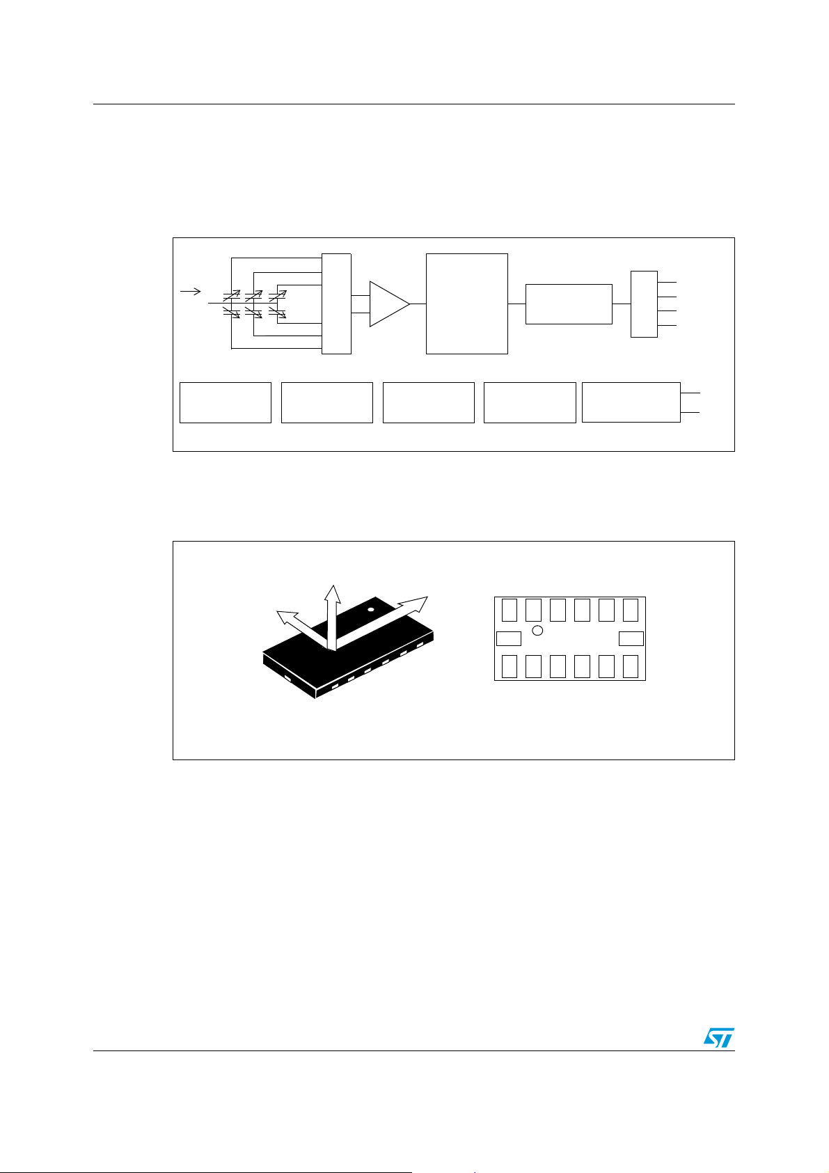
1 Block diagram and pin description
1.1 Block diagram
Figure 1. Block diagram
X+
Y+
Z+
a
MUX
Z-
Y-
X-
CHARGE
AMPLIFIER
A/D
CONVERTER
CONTROL LOGIC
I2C
SPI
CS
SCL/SPC
SDA/SDO/SDI
SDO
REFERENCESELF TEST
1.2 Pin description
Figure 2. Pin connection
Y
6
TOP VIEW
TRIMMING
CIRCUITS
Z
1
CLOCK
1
CONTROL LOGIC
&
INTERRUPT GEN.
6
INT 1
INT 2
X
13
8
13 8
BOTTOM VIEW
8/42
LIS302DL Block diagram and pin description
Table 2. Pin description
Pin# Name Function
1 Vdd_IO Power supply for I/O pins
2 GND 0V supply
3 Reserved Connect to Vdd
4 GND 0V supply
5 GND 0V supply
6 Vdd Power supply
7CS
SPI enable
2
C/SPI mode selection (1: I2C mode; 0: SPI enabled)
I
8 INT 1 Inertial interrupt 1
9 INT 2 Inertial interrupt 2
10 GND 0V supply
11 Reserved Connect to Gnd
12 SDO
SDA
13
SDI
SDO
14
SCL
SPC
SPI Serial Data Output
2
I
C less significant bit of the device address
2
C Serial Data (SDA)
I
SPI Serial Data Input (SDI)
3-wire Interface Serial Data Output (SDO)
2
C Serial Clock (SCL)
I
SPI Serial Port Clock (SPC)
9/42
Mechanical and electrical specifications LIS302DL
2 Mechanical and electrical specifications
2.1 Mechanical characteristics
Table 3. Mechanical characteristics
(1)
(All the parameters are specified @ Vdd=2.5 V, T = 25°C unless otherwise noted)
Symbol Parameter Test conditions Min. Typ.
FS Measurement range
So Sensitivity
(3)
FS bit set to 0 ±2.0 ±2.3
FS bit set to 1 ±8.0 ±9.2
FS bit set to 0 16.2 18 19.8
FS bit set to 1 64.8 72 79.2
TCSO
Ty Of f
TCOff
Sensitivity change vs
temperature
Typical zero-g level offset
accuracy
(4),(5)
Zero-g level change vs
temperature
FS bit set to 0 ±0.01 %/°C
FS bit set to 0 ±40 mg
FS bit set to 1 ±60 mg
Max delta from 25°C
FS bit set to 0
STP bit used
-32 -3 LSb
X axis
FS bit set to 0
STP bit used
Y axis
332LSb
Vst
Self test output
(6),(7),(8),(9)
change
FS bit set to 0
STP bit used
332LSb
Z axis
BW System bandwidth
(10)
Top Operating temperature range -40 +85 °C
Wh Product weight 30 mgram
1. The product is factory calibrated at 2.5V. The device can be used from 2.16V to 3.6V
2. Typical specifications are not guaranteed
3. Verified by wafer level test and measurement of initial offset and sensitivity
4. Typical zero-g level offset value after MSL3 preconditioning
5. Offset can be eliminated by enabling the built-in high pass filter
6. If STM bit is used values change in sign for all axes
7. Self Test output changes with the power supply. Vst at 3.3V is typically in the range [-74; -7] LSb for X axis and [7;74] LSb for Y
and Z axes.
8.
“Self Test Output Change” is defined as OUTPUT[LSb]
1LSb=4.6g/256 at 8bit representation, ±2.3g Full-Scale
9. Output data reach 99% of final value after 3/ODR when enabling Self-Test mode due to device filtering
10. ODR is output data rate. Refer to Table 4 for specifications
(Self-test bit on ctrl_reg1=1)
-OUTPUT[LSb]
(2)
Max. Unit
±0.5 mg/°C
ODR/2 Hz
(Self-test bit on ctrl_reg1=0)
.
mg/digit
g
10/42
LIS302DL Mechanical and electrical specifications
2.2 Electrical characteristics
Table 4. Electrical characteristics
(1)
(All the parameters are specified @ Vdd=2.5 V, T= 25°C unless otherwise noted)
Symbol Parameter Test conditions Min. Typ.
Vdd Supply voltage 2.16 2.5 3.6 V
Vdd_IO I/O pins supply voltage
(3)
1.71 Vdd+0.1 V
Idd Supply current T = 25°C, ODR=100Hz 0.3 0.4 mA
IddPdn
VIH
Current consumption in
power-down mode
Digital high level input
voltage
T = 25°C 1 5 µA
0.8*Vdd
_IO
VIL Digital low level input voltage
VOH High level output voltage
0.9*Vdd
_IO
VOL Low level output voltage
DR=0 100
ODR Output data rate
DR=1 400
BW System bandwidth
Ton Turn-on time
(4)
(5)
Top Operating temperature range -40 +85
1. The product is factory calibrated at 2.5V. The device can be used from 2.16V to 3.6V
2. Typical specification are not guaranteed
3. It is possible to remove Vdd maintaining Vdd_IO without blocking the communication busses, in this condition the
measurement chain is powered off.
4. Filter cut-off frequency
5. Time to obtain valid data after exiting Power-Down mode
(2)
Max. Unit
0.2*Vdd
_IO
0.1*Vdd
_IO
ODR/2 Hz
3/ODR s
V
V
V
V
Hz
°C
11/42
Mechanical and electrical specifications LIS302DL
t
t
t
t
t
t
t
t
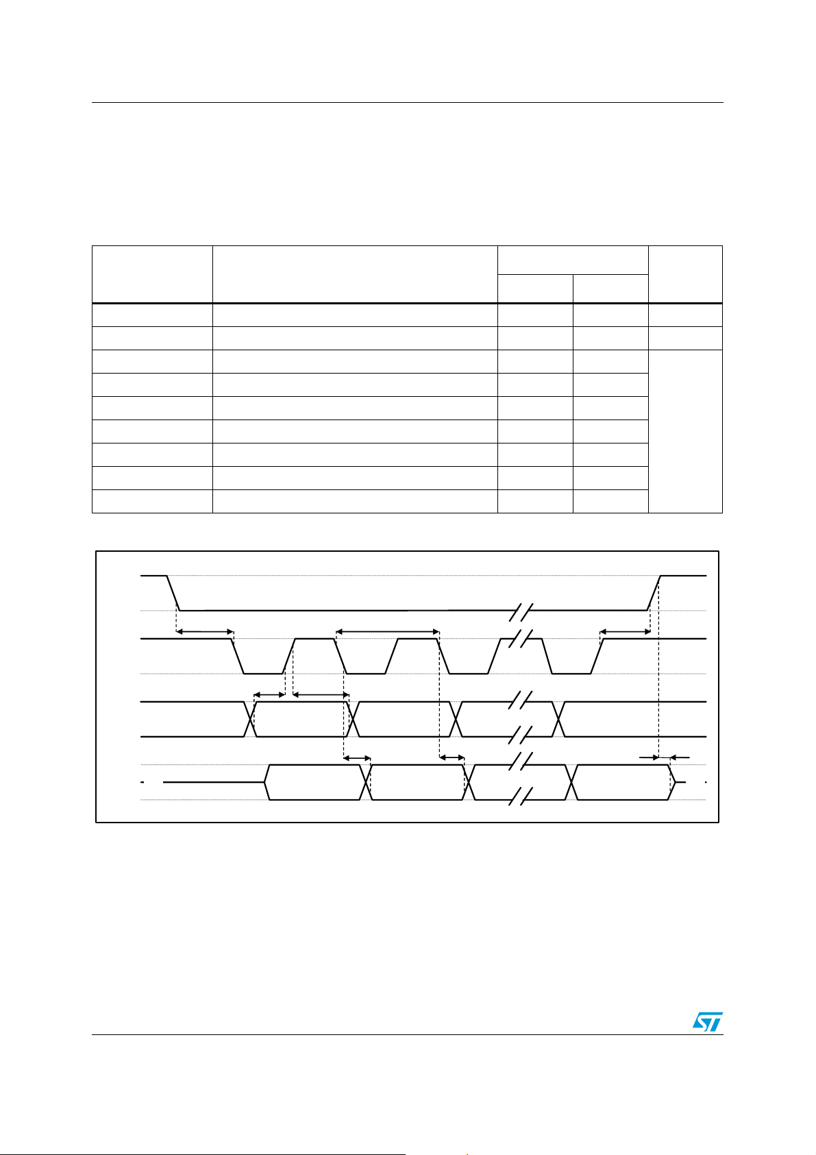
2.3 Communication interface characteristics
2.3.1 SPI - Serial Peripheral Interface
Subject to general operating conditions for Vdd and Top.
Table 5. SPI slave timing values
(1)
Val ue
Symbol Parameter
Min. Max.
tc(SPC) SPI clock cycle 100 ns
fc(SPC) SPI clock frequency 10 MHz
tsu(CS) CS setup time 5
th(CS) CS hold time 8
tsu(SI) SDI input setup time 5
Unit
th(SI) SDI input hold time 15
tv(SO) SDO valid output time 50
th(SO) SDO output hold time 6
tdis(SO) SDO output disable time 50
(2)
c(SPC)
h(SO)
CS
SPC
SDI
SDO
Figure 3. SPI slave timing diagram
(3)
su(CS)
(3)
h(SI)
MSB OUT
(3)
(3)
su(SI)
MSB IN
v(SO)
h(CS)
LSB IN
LSB OUT
ns
(3)
(3)
(3)
dis(SO)
(3)
1. Values are guaranteed at 10MHz clock frequency for SPI with both 4 and 3 wires, based on characterization results, not
tested in production
2. Measurement points are done at 0.2·Vdd_IO and 0.8·Vdd_IO, for both Input and Output port
3. When no communication is on-going, data on CS, SPC, SDI and SDO are driven by internal pull-up resistors
12/42
LIS302DL Mechanical and electrical specifications
t
t
t
t
t
t
t
t
t
t
t
t
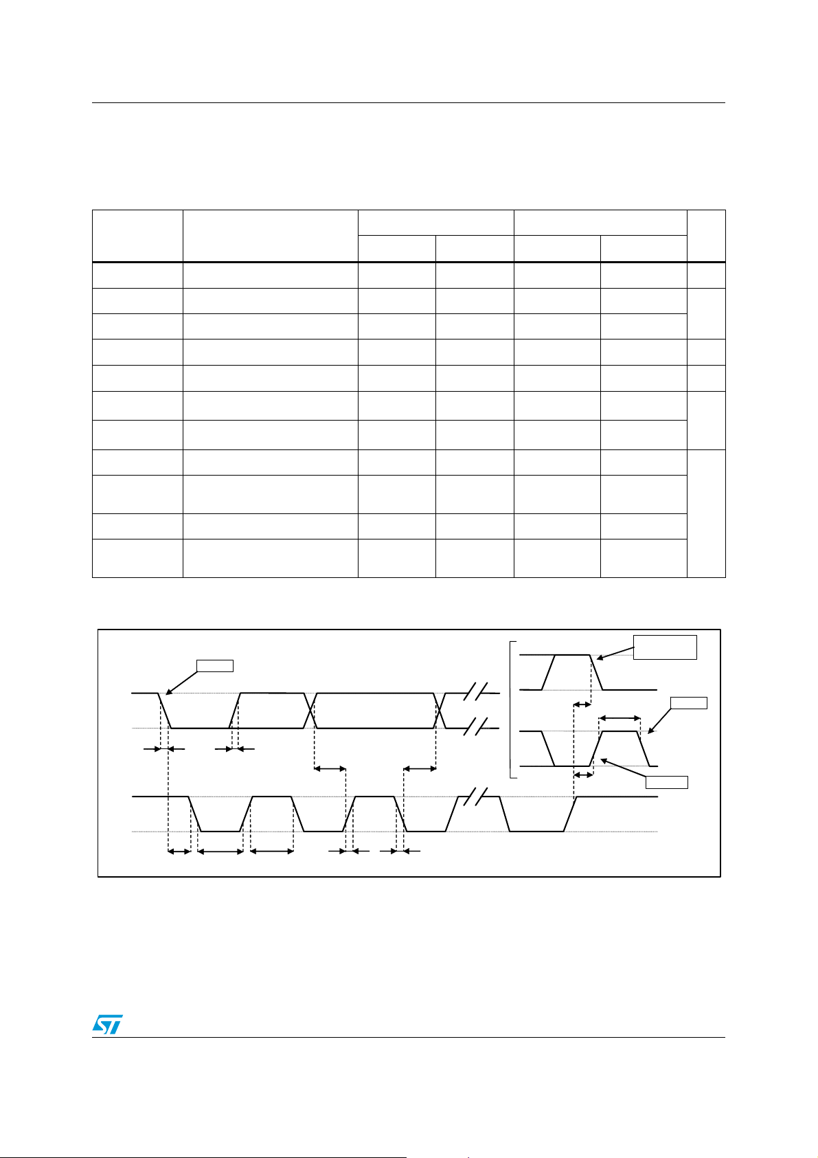
2.3.2 I2C - inter IC control interface
Subject to general operating conditions for Vdd and Top.
Table 6. I
2
C slave timing values
Symbol Parameter
f
(SCL)
t
w(SCLL)
t
w(SCLH)
t
su(SDA)
t
h(SDA)
t
r(SDA) tr(SCL)
t
f(SDA) tf(SCL)
t
h(ST)
t
su(SR)
t
su(SP)
t
w(SP:SR)
SCL clock frequency 0 100 0 400 KHz
SCL clock low time 4.7 1.3
SCL clock high time 4.0 0.6
SDA setup time 250 100 ns
SDA data hold time 0
SDA and SCL rise time 1000
SDA and SCL fall time 300
START condition hold time 4 0.6
Repeated START condition
setup time
STOP condition setup time 4 0.6
Bus free time between STOP
and START condition
I2C standard mode
(1)
I2C fast mode
Min Max Min Max
3.45
(2)
0
20 + 0.1C
20 + 0.1C
(3)
b
(3)
b
4.7 0.6
4.7 1.3
(1)
0.9
300
300
(2)
Unit
µs
µs
ns
µs
SDA
Figure 4. I
f(SDA)
START
2
C Slave timing diagram
r(SDA)
su(SDA)
(4)
h(SDA)
su(SR)
su(SP)
w(SP:SR)
REPEATED
START
START
STOP
SCL
h(ST)
1. Data based on standard I
2. A device must internally provide an hold time of at least 300ns for the SDA signal (referred to VIHmin of the SCL signal) to
bridge the undefined region of the falling edge of SCL
3. Cb = total capacitance of one bus line, in pF
4. Measurement points are done at 0.2·Vdd_IO and 0.8·Vdd_IO, for both port
w(SCLL)
2
C protocol requirement, not tested in production
w(SCLH)
r(SCL)
f(SCL)
13/42
 Loading...