

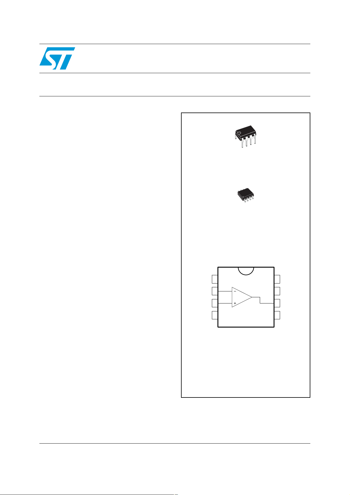
Wide bandwidth single JFET operational amplifiers
8
6
5
7
Features
■ Internally adjustable input offset voltage
■ Low power consumption
■ Wide common-mode (up to V
differential voltage range
■ Low input bias and offset current
■ Output short-circuit protection
■ High input impedance JFET input stage
■ Internal frequency compensation
■ Latch up free operation
■ High slew rate 16 V/µs (typical)
Description
CC
+
) and
LF351
N
DIP8
(Plastic package)
D
SO-8
(Plastic micro package)
These circuits are high speed JFET input single
operational amplifiers incorporating well matched,
high voltage JFET and bipolar transistors in a
monolithic integrated circui t.
The devices feature high slew rates, low input
bias and offset currents, and low offset voltage
temperature coefficient.
Pin connections
(top view)
1
2
3
4
1 - Offset null 1
2 - Inverting input
3 - Non-inverting input
-
4 - V
CC
5 - Offset null 2
6 - Output
+
7 - V
CC
8 - N.C.
April 2008 Rev 2 1/14
www.st.com
14
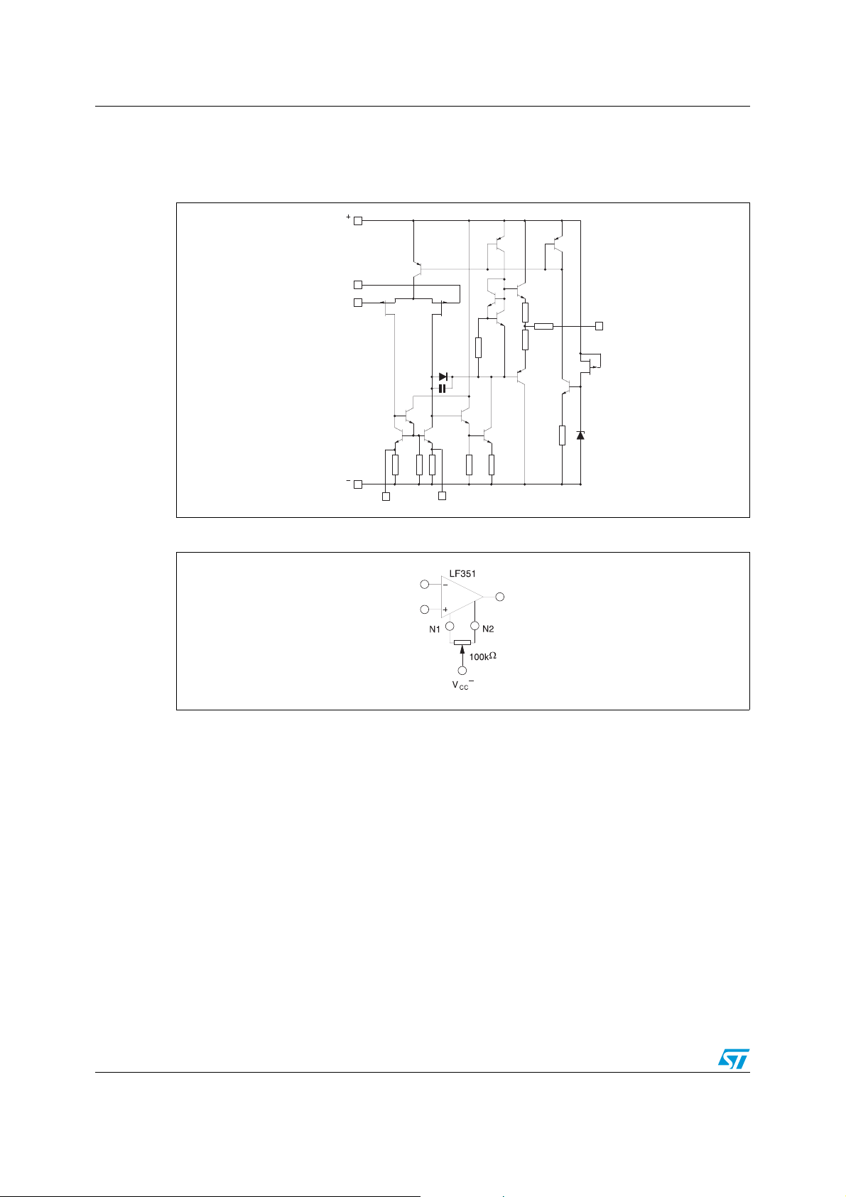
Schematics LF351
1 Schematics
Figure 1. Schematic diagram
V
CC
Non-inverting
input
input
Inverting
1.3k
V
CC
Offset Null1 Offset Null2
1.3k
35k
W
100
W
200
W
100
30k
8.2k
W
100
35k
Output
Figure 2. Input offset voltage null circuit
2/14
LF351 Absolute maximum ratings and operating conditions
2 Absolute maximum ratings and operating conditions
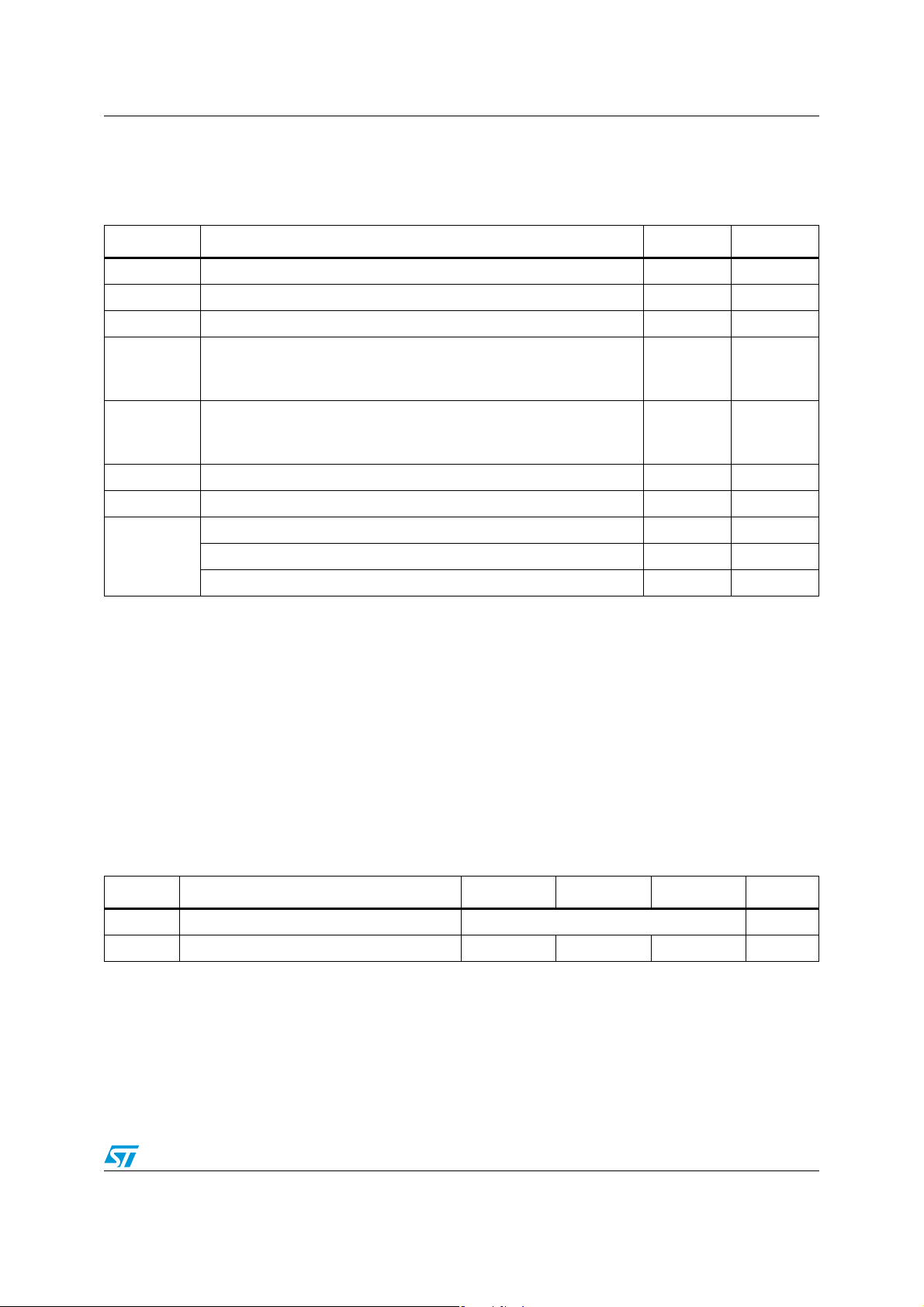
Table 1. Absolute maximum ratings
Symbol Parameter Value Unit
(2)
(1)
(7)
(3)
(6)
(5)
(8)
(4)
CC
(4)
+
and V
CC
±18 V
±15 V
±30 V
125
°C/W
85
40
°C/W
41
Infinite
500 V
200 V
1.5 kV
-
.
V
CC
V
i
V
id
Supply voltage
Input voltage
Differential input voltage
Thermal resistance junction to ambient
R
thja
SO-8
DIP8
Thermal resistance junction to case
R
thjc
SO-8
DIP8
Output short-circuit duration
T
stg
Storage temperature range -65 to +150 °C
HBM: human body model
ESD
MM: machine model
CDM: charged device model
1. All voltage values, except differential voltage, are with respect to the zero reference level (ground) of the supply voltages
where the zero reference level is the midpoint between V
2. The magnitude of the input voltage must never exceed the magnitude of the supply voltage or 15 volts, whichever is less.
3. Differential voltages are the non-inverting input terminal with respect to the inverting input terminal.
4. Short-circuits can cause excessive heating and destructive dissipation. Values are typical.
5. The output may be shorted to ground or to either supply. Temperature and/or supply voltages must be limited to ensure
that the dissipation rating is not exceeded
6. Human body model: A 100 pF capacitor is charged to the specified voltage, then discharged through a 1.5 kΩ resistor
between two pins of the device. This is done for all couples of connected pin combinations while the other pins are floating.
7. Machine model: A 200 pF capacitor is charged to the specified voltage, then discharged directly between two pins of the
device with no external series resistor (internal resistor < 5 Ω). This is done for all couples of connected pin combinations
while the other pins are floating.
8. Charged device model: all pins and the package are charged together to the specified voltage and then discharged directly
to the ground through only one pin. This is done for all pins.
Table 2. Operating conditions
Symbol Parameter LF151 LF251 LF351 Unit
T
V
oper
Supply voltage 6 to 32 V
CC
Operating free-air temperature range -55 to +125 -40 to +105 0 to +70 °C
3/14
Electrical characteristics LF351
3 Electrical characteristics
Table 3. Electrical characteristics at VCC = ±15 V, T
= +25°C (unless otherwise specified)
amb
Symbol Parameter Min. Typ. Max. Unit
V
io
DV
I
io
I
ib
A
vd
SVR
I
CC
V
icm
CMR
I
OS
Input offset voltage (Rs = 10kΩ)
≤ T
≤ T
≤ T
amb
amb
amb
≤ T
≤ T
≤ T
max
max
(1)
max
(1)
T
min
Input offset voltage drift 10 µV/°C
io
Input offset current
T
min
Input bias current
T
min
Large signal voltage gain (RL = 2kΩ, Vo = ±10V)
T
≤ T
≤ T
amb
amb
≤ T
≤ T
max
max
= 10kΩ)
S
min
Supply voltage rejection ratio (R
T
min
Supply current, no load
≤ T
T
min
amb
≤ T
max
Input common mode voltage range
Common mode rejection ratio (RS = 10kΩ)
T
≤ T
amb
≤ T
max
min
Output short-circuit current
T
≤ T
amb
≤ T
max
min
310
5 100
20 200
5025200
808086
1.4 3.4
±11 +15
-12
707086
101040 60
13
4
20
V/mV
3.4
60
Output voltage swing
RL = 2kΩ
= 10kΩ
R
±V
opp
L
≤ T
T
min
amb
≤ T
max
RL = 2kΩ
= 10kΩ
R
L
SR Slew rate, V
Rise time, Vi = 20mV, RL = 2kΩ, CL = 100pF, unity gain 0.1 µs
t
r
K
Overshoot, Vi = 20mV, RL = 2kΩ, CL = 100pF, unity gain 10 %
ov
= 10V, RL = 2kΩ, CL = 100pF, unity gain 12 16 V/µs
i
GBP Gain bandwidth product, f = 100kHz, V
Input resistance 10
R
i
THD
Total harmonic distortion
f= 1kHz, A
Equivalent input noise voltage
e
n
R
S
= 20dB, RL= 2kΩ, CL=100pF, Vo=2V
v
= 100Ω, f = 1KHz
= 10mV, RL = 2kΩ, CL = 100pF 2.5 4 MHz
in
pp
10
12
12
13.5
10
12
12
0.01 %
15
∅m Phase margin 45 Degrees
mV
pA
nA
pA
nA
dB
mA
V
dB
mA
V
Ω
nV
----------- Hz
1. The input bias currents are junction leakage currents which approximately double for every 10°C increase in the junction
temperature.
4/14
LF351 Electrical characteristics
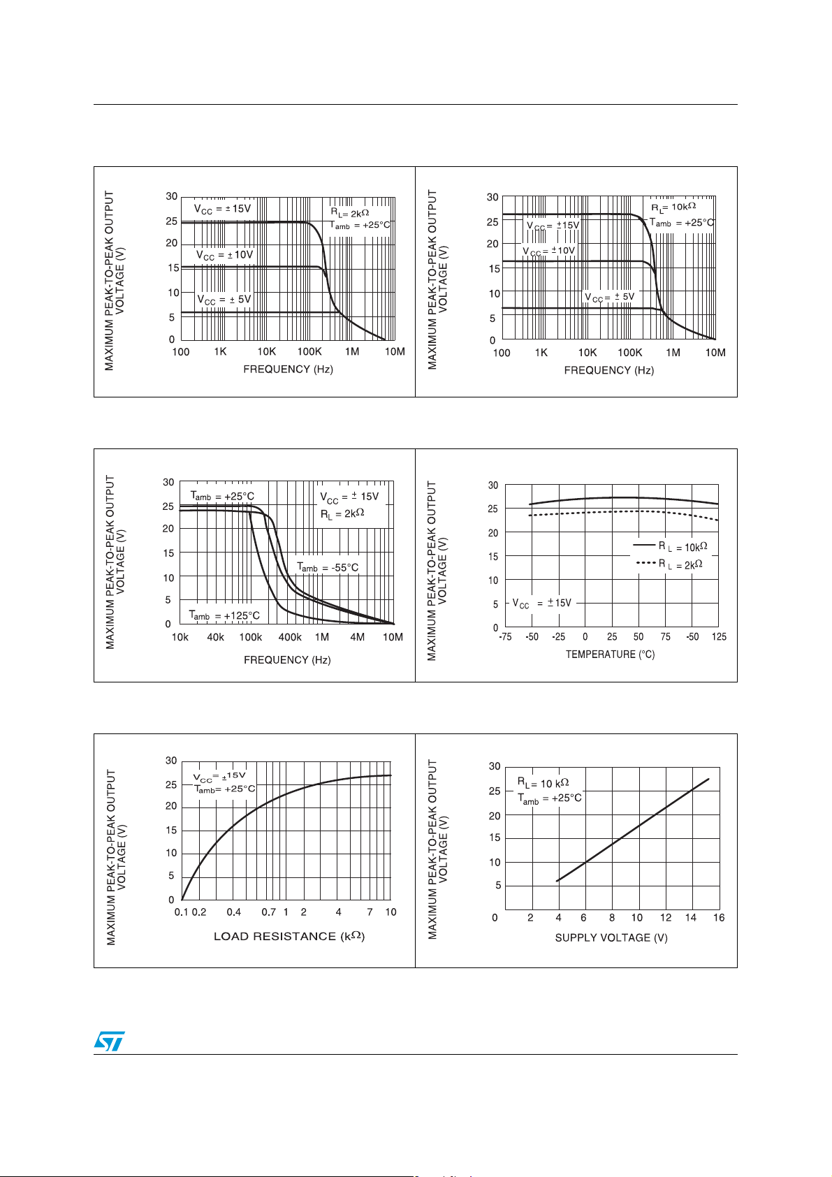
Figure 3. Maximum peak-to-peak output
voltage versus frequency
Figure 5. Maximum peak-to-peak output
voltage versus frequency
Figure 4. Maximum peak-to-peak output
voltage versus frequency
Figure 6. Maximum peak-to-peak output
voltage versus free air temp.
Figure 7. Maximum peak-to-peak output
voltage versus load resistance
Figure 8. Maximum peak-to-peak output
voltage versus supply vo ltage
5/14

Electrical characteristics LF351
Figure 9. Input bias current versus free air
temperature
Figure 11. Large signal differential voltage
amplification and phase shift
versus frequency
Figure 10. Large signal differential voltage
amplification versus free air temp.
Figure 12. Total power dissipation versus free
air temperature
Figure 13. Supply current per amplifier ver sus
free air temperature
6/14
Figure 14. Supply current per ampli fier ver sus
supply voltage

LF351 Electrical characteristics
Figure 15. Common mode rejection ratio
versus free air temperature
Figure 16. Voltage follower large signal pulse
response
Figure 17. Output voltage versus elapsed time Figure 18. Equivalent input noise voltage
versus frequency
Figure 19. Total harmonic distortion versus
frequency
7/14

Parameter measurement information LF351
4 Parameter measurement information
Figure 20. Voltage follower Figure 21. Gain-of-10 inverting amplifier
8/14

LF351 Typical application
5 Typical application
Figure 22. Square wave oscillator (0.5 Hz)
Figure 23. High Q notch filter
9/14

Package information LF351
6 Package information
In order to meet environmental requirements, STMicroelectronics offers these devices in
ECOPACK
category of second level interconnect is marke d on the pa ckage and on the inner box label,
in compliance with JEDEC Standard JESD97. The maximum ratings related t o soldering
conditions are also marked on the inner box label. ECOPACK is an STMicroelectronics
trademark. ECOPACK specifications are available at: www.st.com
®
packages. These packages have a lead-free second level interconnect. The
.
10/14

LF351 Package information
6.1 DIP8 package information
Figure 24. DIP8 package mechanical drawing
Table 4. DIP8 package mechanical data
Dimensions
Ref.
Min. Typ. Max. Min. Typ. Max.
A5.330.210
A1 0.38 0.015
A2 2.92 3.30 4.95 0.115 0.130 0.195
b 0.36 0.46 0.56 0.014 0.018 0.022
b2 1.14 1.52 1.78 0.045 0.060 0.070
c 0.20 0.25 0.36 0.008 0.010 0.014
D 9.02 9.27 10.16 0.355 0.365 0.400
E 7.62 7.87 8.26 0.300 0.310 0.325
E1 6.10 6.35 7.11 0.240 0.250 0.280
e 2.54 0.100
eA 7.62 0.300
eB 10.92 0.430
L 2.92 3.30 3.81 0.115 0.130 0.150
Millimeters Inches
11/14

Package information LF351
6.2 SO-8 package information
Figure 25. SO-8 package mechanical drawing
Table 5. SO-8 package mechanical data
Dimensions
Ref.
Min. Typ. Max. Min. Typ. Max.
A1.750.069
A1 0.10 0.25 0.004 0.010
A2 1.25 0.049
b 0.28 0.48 0.011 0.019
c 0.17 0.23 0.007 0.010
D 4.80 4.90 5.00 0.189 0.193 0.197
E 5.80 6.00 6.20 0.228 0.236 0.244
E1 3.80 3.90 4.00 0.150 0.154 0.157
e 1.27 0.050
h 0.25 0.50 0.010 0.020
L 0.40 1.27 0.016 0.050
k1°8°1°8°
ccc 0.10 0.004
Millimeters Inches
12/14

LF351 Ordering information
7 Ordering information
Table 6. Order codes
Order code
LF151N
LF151D
LF151DT
LF251N
LF251D
LF251DT
LF351N
LF351D
LF351DT
Temperature
range
-55°C, +125°C
-40°C, +105°C
0°C, +70°C
8 Revision history
Table 7. Document revision history
Date Revision Changes
17-May-2001 1 Initial release.
Package Packing Marking
DIP8 Tape LF151N
SO-8
DIP8 Tape LF251N
SO-8
DIP8 Tape LF351N
SO-8
Tape or
Tape & reel
Tape or
Tape & reel
Tape or
Tape & reel
151
251
351
28-April-2008 2 Updated document format.
13/14

LF351
Please Read Carefully:
Information in this document is provided solely in connection with ST products. STMicroelectronics NV and its subsidiaries (“ST”) reserve the
right to make changes, corrections, modifications or improvements, to this document, and the products and services described herein at any
time, without notice.
All ST products are sold pursuant to ST’s terms and conditions of sale.
Purchasers are solely res ponsibl e fo r the c hoic e, se lecti on an d use o f the S T prod ucts and s ervi ces d escr ibed he rein , and ST as sumes no
liability whatsoever relati ng to the choice, selection or use of the ST products and s ervices described herein.
No license, express or implied, by estoppel or otherwise, to any intellectual property rights is granted under this document. If any part of this
document refers to any third pa rty p ro duc ts or se rv ices it sh all n ot be deem ed a lice ns e gr ant by ST fo r t he use of su ch thi r d party products
or services, or any intellectua l property c ontained the rein or consi dered as a warr anty coverin g the use in any manner whats oever of suc h
third party products or servi ces or any intellectual property contained therein .
UNLESS OTHERWISE SET FORTH IN ST’S TERMS AND CONDITIONS OF SALE ST DISCLAIMS ANY EXPRESS OR IMPLIED
WARRANTY WITH RESPECT TO THE USE AND/OR SALE OF ST PRODUCTS INCLUDING WITHOUT LIMITATION IMPLIED
WARRANTIES OF MERCHANTABILITY, FITNESS FOR A PARTICUL AR PURPOS E (AND THEIR EQUIVALE NTS UNDER THE LAWS
OF ANY JURISDICTION), OR INFRINGEMENT OF ANY PATENT, COPYRIGHT OR OTHER INTELLECTUAL PROPERTY RIGHT.
UNLESS EXPRESSLY APPROVED IN WRITING BY AN AUTHORIZED ST REPRESENTATIVE, ST PRODUCTS ARE NOT
RECOMMENDED, AUTHORIZED OR WARRANTED FOR USE IN MILITARY, AIR CRAFT, SPACE, LIFE SAVING, OR LIFE SUSTAINING
APPLICATIONS, NOR IN PRODUCTS OR SYSTEMS WHERE FAILURE OR MALFUNCTION MAY RESULT IN PERSONAL INJ URY,
DEATH, OR SEVERE PROPERTY OR ENVIRONMENTAL DAMAGE. ST PRODUCTS WHICH ARE NOT SPECIFIED AS "AUTOMOTIVE
GRADE" MAY ONLY BE USED IN AUTOMOTIVE APPLICATIONS AT USER’S OWN RISK.
Resale of ST products with provisions different from the statements and/or technical features set forth in this document shall immediately void
any warranty granted by ST fo r the ST pro duct or serv ice describe d herein and shall not cr eate or exten d in any manne r whatsoever , any
liability of ST.
ST and the ST logo are trademarks or registered trademarks of ST in various countries.
Information in this document su persedes and replaces all information previously supplied.
The ST logo is a registered trademark of STMicroelectronics. All other names are the property of their respective owners.
© 2008 STMicroelectronics - All rights reserved
STMicroelectronics group of compan ie s
Australia - Belgium - Brazil - Canada - China - Czech Republic - Finland - France - Germany - Hong Kong - India - Israel - Italy - Japan -
Malaysia - Malta - Morocco - Singapore - Spain - Sweden - Switzerland - United Kingdom - United States of America
www.st.com
14/14
 Loading...