

ST LED7706 User Manual
6-rows 30 mA LEDs driver with boost regulator
Features
■ Boost section
– 4.5 V to 36 V input voltage range
– Internal power MOSFET
– Internal +5 V LDO for device supply
– Up to 36 V output voltage
– Constant frequency peak current-mode
control
– 250 kHz to 1 MHz adjustable switching
frequency
– External synchronization for multi-device
application
– Pulse-skip power saving mode at light load
– Programmable soft-start
– Programmable OVP protection
– Stable with ceramic output capacitors
– Thermal shutdown
■ Backlight driver section
– Six rows with 30 mA maximum current
capability (adjustable)
– Rows disable option
– Less than 500 ns minimum dimming on-
time (1 % minimum dimming duty-cycle at
20 kHz)
– ±2 % current matching between rows
– LED failure (open and short-circuit)
detection
LED7706
for LCD panels backlight
VFQFPN-24 4x4
Description
The LED7706 consists of a high efficiency
monolithic boost converter and six controlled
current generators (rows) specifically designed to
supply LEDs arrays used in the backlighting of
LCD panels. The device can manage an output
voltage up to 36 V (i.e. 10 white LEDs per row).
The generators can be externally programmed to
sink up to 30 mA and can be dimmed via a PWM
signal (1 % dimming duty-cycle at 20 kHz can be
managed). The device allows to detect and
manage the open and shorted LED faults and to
let unused rows floating. Basic protections (output
over-voltage, internal MOSFET over-current and
thermal shutdown) are provided.
Applications
■ LCD monitors and TV panels
■ PDAs panel backlight
■ GPS panel backlight
Table 1. Device summary
Order codes Package Packaging
LED7706
VFQFPN-24 4x4 (exposed pad)
LED7706TR Tape and reel
April 2009 Rev 2 1/46
Tu b e
www.st.com
46

Contents LED7706
Contents
1 Typical application circuit . . . . . . . . . . . . . . . . . . . . . . . . . . . . . . . . . . . . 4
2 Pin settings . . . . . . . . . . . . . . . . . . . . . . . . . . . . . . . . . . . . . . . . . . . . . . . . 5
2.1 Connections . . . . . . . . . . . . . . . . . . . . . . . . . . . . . . . . . . . . . . . . . . . . . . . . 5
2.2 Pin description . . . . . . . . . . . . . . . . . . . . . . . . . . . . . . . . . . . . . . . . . . . . . . 6
3 Electrical data . . . . . . . . . . . . . . . . . . . . . . . . . . . . . . . . . . . . . . . . . . . . . . 7
3.1 Maximum rating . . . . . . . . . . . . . . . . . . . . . . . . . . . . . . . . . . . . . . . . . . . . . 7
3.2 Thermal data . . . . . . . . . . . . . . . . . . . . . . . . . . . . . . . . . . . . . . . . . . . . . . . 7
4 Electrical characteristics . . . . . . . . . . . . . . . . . . . . . . . . . . . . . . . . . . . . . 8
5 Operation description . . . . . . . . . . . . . . . . . . . . . . . . . . . . . . . . . . . . . . . 10
5.1 Boost section . . . . . . . . . . . . . . . . . . . . . . . . . . . . . . . . . . . . . . . . . . . . . . 11
5.1.1 Functional description . . . . . . . . . . . . . . . . . . . . . . . . . . . . . . . . . . . . . . 11
5.1.2 Enable function . . . . . . . . . . . . . . . . . . . . . . . . . . . . . . . . . . . . . . . . . . . 12
5.1.3 Soft-start . . . . . . . . . . . . . . . . . . . . . . . . . . . . . . . . . . . . . . . . . . . . . . . . 13
5.1.4 Overvoltage protection . . . . . . . . . . . . . . . . . . . . . . . . . . . . . . . . . . . . . . 14
5.1.5 Switching frequency selection and synchronization . . . . . . . . . . . . . . . 15
5.1.6 Slope compensation . . . . . . . . . . . . . . . . . . . . . . . . . . . . . . . . . . . . . . . 16
5.1.7 Boost current limit . . . . . . . . . . . . . . . . . . . . . . . . . . . . . . . . . . . . . . . . . 18
5.1.8 Thermal protection . . . . . . . . . . . . . . . . . . . . . . . . . . . . . . . . . . . . . . . . . 18
5.2 Backlight driver section . . . . . . . . . . . . . . . . . . . . . . . . . . . . . . . . . . . . . . 19
5.2.1 Current generators . . . . . . . . . . . . . . . . . . . . . . . . . . . . . . . . . . . . . . . . . 19
5.2.2 PWM dimming . . . . . . . . . . . . . . . . . . . . . . . . . . . . . . . . . . . . . . . . . . . . 20
5.3 Fault management . . . . . . . . . . . . . . . . . . . . . . . . . . . . . . . . . . . . . . . . . . 21
5.3.1 FAULT pin . . . . . . . . . . . . . . . . . . . . . . . . . . . . . . . . . . . . . . . . . . . . . . . 21
5.3.2 MODE pin . . . . . . . . . . . . . . . . . . . . . . . . . . . . . . . . . . . . . . . . . . . . . . . 21
5.3.3 Open LED fault . . . . . . . . . . . . . . . . . . . . . . . . . . . . . . . . . . . . . . . . . . . 22
5.3.4 Shorted LED fault . . . . . . . . . . . . . . . . . . . . . . . . . . . . . . . . . . . . . . . . . 23
2/46

LED7706 Contents
6 Application information . . . . . . . . . . . . . . . . . . . . . . . . . . . . . . . . . . . . . 24
6.1 System stability . . . . . . . . . . . . . . . . . . . . . . . . . . . . . . . . . . . . . . . . . . . . 24
6.1.1 Loop compensation . . . . . . . . . . . . . . . . . . . . . . . . . . . . . . . . . . . . . . . . 24
6.2 Thermal considerations . . . . . . . . . . . . . . . . . . . . . . . . . . . . . . . . . . . . . . 27
6.3 Component selection . . . . . . . . . . . . . . . . . . . . . . . . . . . . . . . . . . . . . . . . 28
6.3.1 Inductor selection . . . . . . . . . . . . . . . . . . . . . . . . . . . . . . . . . . . . . . . . . . 28
6.3.2 Capacitors selection . . . . . . . . . . . . . . . . . . . . . . . . . . . . . . . . . . . . . . . 29
6.3.3 Flywheel diode selection . . . . . . . . . . . . . . . . . . . . . . . . . . . . . . . . . . . . 29
6.4 Design example . . . . . . . . . . . . . . . . . . . . . . . . . . . . . . . . . . . . . . . . . . . . 30
6.4.1 Switching frequency setting . . . . . . . . . . . . . . . . . . . . . . . . . . . . . . . . . . 30
6.4.2 Row current setting . . . . . . . . . . . . . . . . . . . . . . . . . . . . . . . . . . . . . . . . 30
6.4.3 Inductor choice . . . . . . . . . . . . . . . . . . . . . . . . . . . . . . . . . . . . . . . . . . . 30
6.4.4 Output capacitor choice . . . . . . . . . . . . . . . . . . . . . . . . . . . . . . . . . . . . . 31
6.4.5 Input capacitor choice . . . . . . . . . . . . . . . . . . . . . . . . . . . . . . . . . . . . . . 33
6.4.6 Over-voltage protection divider setting . . . . . . . . . . . . . . . . . . . . . . . . . 33
6.4.7 Compensation network . . . . . . . . . . . . . . . . . . . . . . . . . . . . . . . . . . . . . 34
6.4.8 Boost current limit . . . . . . . . . . . . . . . . . . . . . . . . . . . . . . . . . . . . . . . . . 34
6.4.9 Power dissipation estimate . . . . . . . . . . . . . . . . . . . . . . . . . . . . . . . . . . 35
6.5 Layout consideration . . . . . . . . . . . . . . . . . . . . . . . . . . . . . . . . . . . . . . . . 37
7 Electrical characteristics . . . . . . . . . . . . . . . . . . . . . . . . . . . . . . . . . . . . 41
8 Package mechanical data . . . . . . . . . . . . . . . . . . . . . . . . . . . . . . . . . . . . 43
9 Revision history . . . . . . . . . . . . . . . . . . . . . . . . . . . . . . . . . . . . . . . . . . . 45
3/46
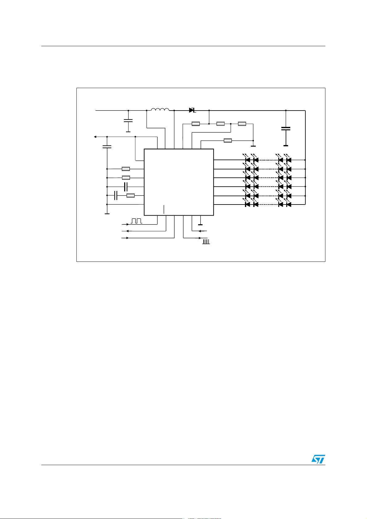
Typical application circuit LED7706
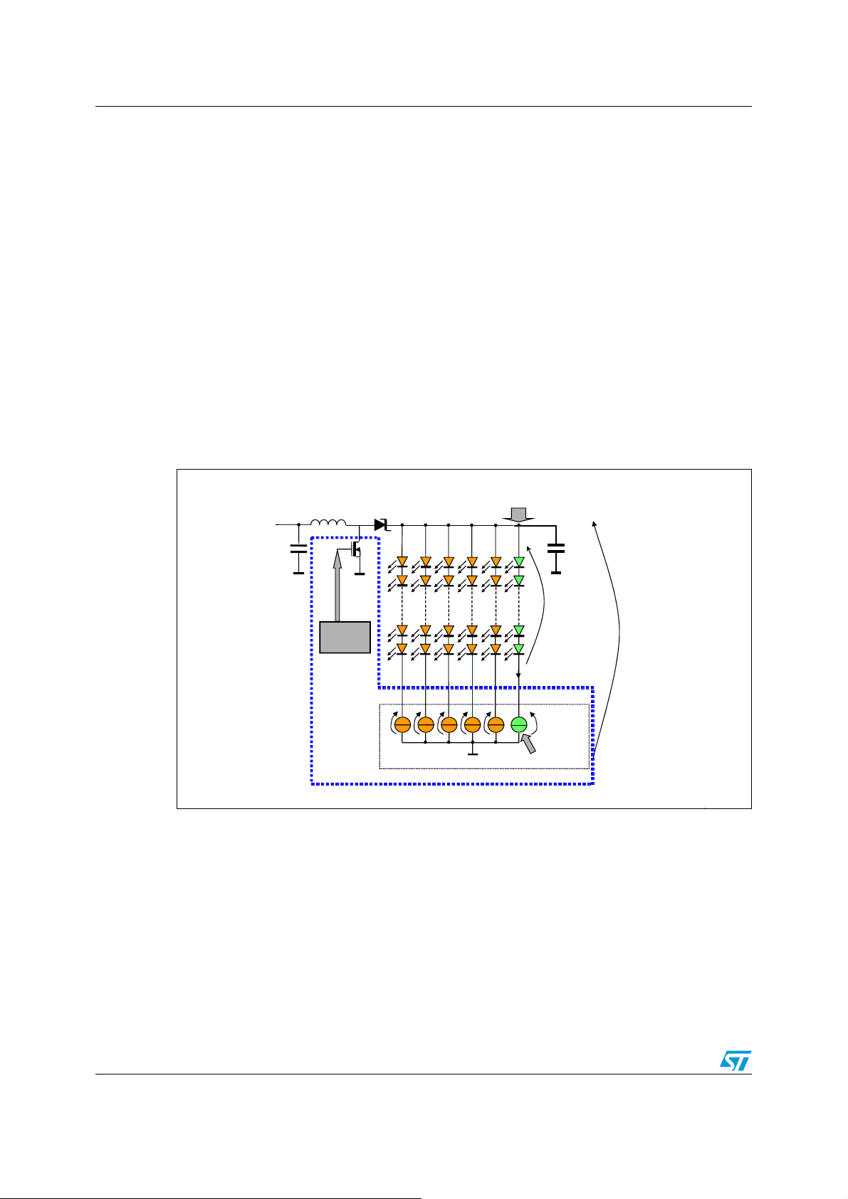
1 Typical application circuit
Figure 1. Application circuit
VIN
+5V
Internal MOS OCP
Rows current selection
Dimming
Fault
Enable
LDO5
BILIM
RILIM
SS
COMP
SGND
L
LX
VIN
AVCC
LED7706
FAULT
DIM
EN
Slope Compensation
OVSEL
SLOPE
MODE
SYNC
OVP selection
Switching Frequenc y selection
SWF
ROW1
ROW2
ROW3
ROW4
ROW5
ROW6
PGND
Faults Management Selection
Sync Output
MLCC
Up to 10 WLEDs per row
OUT
V
AM00594v1
4/46
LED7706 Pin settings
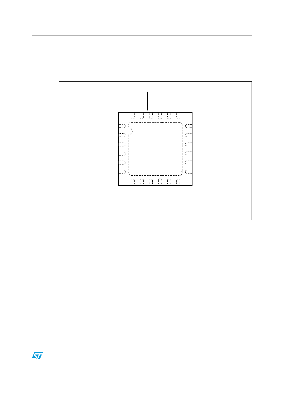
2 Pin settings
2.1 Connections
Figure 2. Pin connection (through top view)
COMP
RILIM
BILIM
FSW
MODE
AVCC
SYNC
SS
24
1
EN
DIM
FAULT
LX
19
18
OVSEL
PGND
LED7706
ROW6
ROW5
ROW4
ROW3
6
7
13
12
VIN
LDO5
SGND
SLOPE
ROW2
ROW1
AM00595v1
5/46

Pin settings LED7706
2.2 Pin description
Table 2. Pin functions
N° Pin Function
1COMP
2RILIM
3 BILIM
4FSW
5MODE
6 AVCC + 5 V analog supply. Connect to LDO5 through a simple RC filter.
7LDO5
8 VIN Input voltage. Connect to the main supply rail.
9SLOPE
10 SGND
11 ROW1 Row driver output #1.
Error amplifier output. A simple RC series between this pin and ground is
needed to compensate the loop of the boost regulator.
Output generators current limit setting. The output current of the rows can be
programmed connecting a resistor to SGND.
Boost converter current limit setting. The internal MOSFET current limit can
be programmed connecting a resistor to SGND.
Switching frequency selection and external sync input. A resistor to SGND is
used to set the desired switching frequency. The pin can also be used as
external synchronization input. See
Current generators fault management selector. It allows to detect and manage
LEDs failures. See
+ 5 V LDO output and power section supply. Bypass to SGND with a
1 μF ceramic capacitor.
Slope compensation setting. A resistor between the output of the boost
converter and this pin is needed to avoid sub-harmonic instability.
Refer to
Signal ground. Supply return for the analog circuitry and the current
generators.
Section 6.1 on page 24 for details.
Section 5.3.2 on page 21 for details.
Section 5.1.5 on page 15 for details.
12 ROW2 Row driver output #2.
13 ROW3 Row driver output #3.
14 ROW4 Row driver output #4.
15 ROW5 Row driver output #5.
16 ROW6 Row driver output #6.
17 PGND Power ground. Source of the internal Power MOSFET.
18 OVSEL
19 LX Switching node. Drain of the internal Power MOSFET.
20 DIM Dimming input. Used to externally set the brightness by using a PWM signal.
21 EN
22 FAULT
23 SYNC Synchronization output. Used as external synchronization output.
24 SS Soft-start. Connect a capacitor to SGND to set the desired soft-start duration.
6/46
Over-voltage selection. Used to set the desired OV threshold by an external
divider. See
Enable input. When low, the device is turned off. If tied high or left open, the
device is turned on and a soft-start sequence takes place.
Fault signal output. Open drain output. The pin goes low when a fault condition
is detected (see Section 5.3.1 on page 21 for details).
Section 5.1.4 on page 14 for details.
LED7706 Electrical data
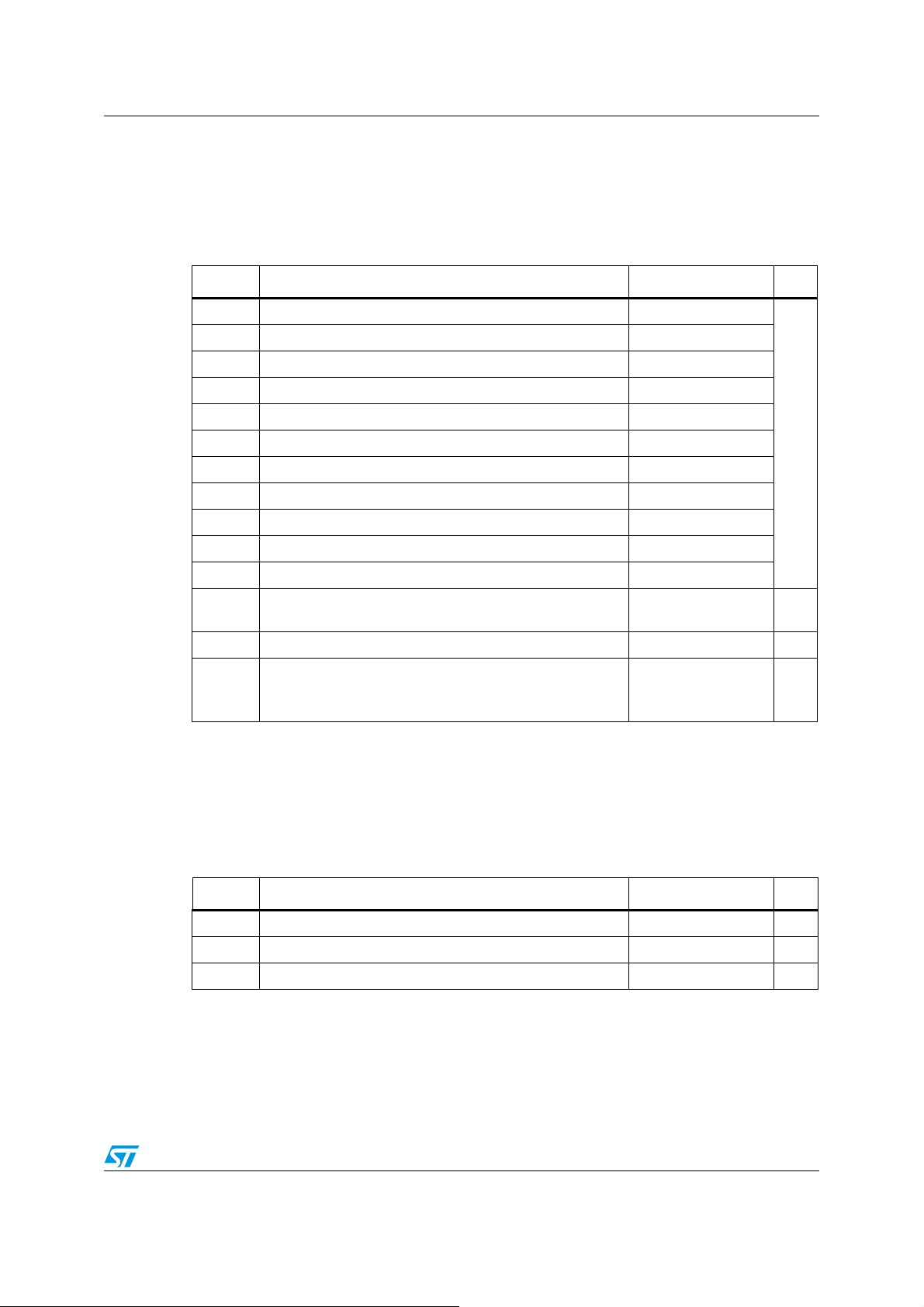
3 Electrical data
3.1 Maximum rating
Table 3. Absolute maximum ratings
(1)
Symbol Parameter Value Unit
V
AVC C
V
LDO5
AVCC to SGND -0.3 to 6
LDO5 to SGND -0.3 to 6
PGND to SGND -0.3 to 0.3
V
V
VIN to PGND -0.3 to 40
IN
LX to SGND -0.3 to 40
LX
LX to PGND -0.3 to 40
RILIM, BILIM, SYNC, OVSEL, SS to SGND -0.3 to V
AVC C
+ 0.3
EN, DIM, SW, MODE, FAULT to SGND -0.3 to 6
ROWx to PGND/ SGND -0.3 to 40
SLOPE to VIN V
- 0.3 to VIN + 6
IN
SLOPE to SGND -0.3 to 40
Internal switch maximum RMS current
(flowing through LX node)
P
Power dissipation @ TA = 25 °C 2.3
TOT
2.0 A
(2)
Maximum withstanding voltage range test condition:
CDF-AEC-Q100-002- “human body model” acceptance
±1000 V
criteria: “normal performance”
1. Stresses beyond those listed under “absolute maximum ratings” may cause permanent damage to the
device. Exposure to absolute maximum rated conditions for extended periods may affect device reliability.
2. Power dissipation referred to the device mounted on the demonstration board described in section 5.5
V
W
3.2 Thermal data
Table 4. Thermal data
Symbol Parameter Value Unit
R
T
Thermal resistance junction to ambient 42 °C/W
thJA
Storage temperature range -50 to 150 °C
STG
Junction operating temperature range -40 to 150 °C
T
J
7/46
Electrical characteristics LED7706
4 Electrical characteristics
VIN = 12 V; TJ = 25 °C and LDO5 connected to AVCC if not otherwise specified
Table 5. Electrical characteristics
(a)
Symbol Parameter Test condition Min. Typ. Max. Unit
Supply section
V
V
V
I
V
BST
LDO5
AVC C
IN,Q
Input voltage range 4.5 36 V
IN
Boost section output voltage 36
LDO output and IC supply
voltage
Operating quiescent current
EN High
= 0 mA
I
LDO5
= 51 kΩ, R
R
RILIM
R
SLOPE
= 680 kΩ
BILIM
4.4 5 5.5 V
= 220 kΩ,
1mA
DIM tied to SGND.
I
IN,SHDN
V
UVLO,ON
V
UVLO,OFF
Operating current in shutdown EN low 20 30 μA
LDO5 under voltage lock out
upper threshold
LDO5 under voltage lock out
lower threshold
3.3 3.6
3.8 4.0
LDO linear regulator
Line regulation 6 V
LDO dropout voltage V
LDO maximum output current
V
V
IN
LDO5
LDO5
≤ 36 V, I
IN
= 4.3 V, I
> V
UVLO,ON
< V
UVLO,OFF
LDO5
= 30 mA 30
LDO5
= 10 mA 80 120
25 40 60
20 30
≤ V
Boost section
V
mV
mA
t
ON,min
f
SW
Minimum switching on-time 200 ns
Default switching frequency FSW connected to AVCC 570 660 750
Minimum FSW sync frequency 210
FSW sync input threshold 240
FSW sync input hysteresis 20
FSW sync min. ON time 270 ns
SYNC output Duty-Cycle
SYNC output high level I
SYNC output low level I
a. Specification referred to TJ from 0 °C to +85 °C. Specification over the 0 to +85 °C TJ range are assured by
design, characterization and statistical correlation.
FSW connected to AVCC
(Internal oscillator selected)
= 10 μA
SYNC
= -10 μA 20
SYNC
8/46
V
AVC C
-20V
kHz
mVFSW sync low level 350
34 40 %
mV
LED7706 Electrical characteristics
Table 5. Electrical characteristics (continued)
Symbol Parameter Test condition Min. Typ. Max. Unit
Power switch
5
V
R
K
DSon
LX current coefficient R
B
Internal MOSFET on-resistance
OC and OV protections
= 600 kΩ 5·1056·1057·10
BILIM
280 500 mΩ
V
TH,OVP
V
TH,FRD
ΔV
OVP,FRD
Over voltage protection
reference threshold (OVSEL)
Floating channel detection
threshold
Voltage gap between OVP and
FRD thresholds
Soft-start and power management
EN, Turn-on threshold 1.6
EN, Turn-off threshold 0.8
DIM, high level threshold 1.3
DIM, low level threshold 0.8
EN, pull-up current 2.5
SS, charge current 4 5 6
SS, end-of-startup threshold 2.0 2.4 2.8
SS, reduced switching
frequency release threshold
Current generators section
T
DIM-
ON,min
K
ΔK
V
IFB
V
rowx,
FAULT
V
FAU LT,
LOW
Minimum dimming on-time 500 ns
Current generators gain 987 V
R
Current generators gain
(1)
R
accuracy
Feedback regulation voltage 400 mV
Shorted LED fault detection
threshold
FAULT pin low-level voltage I
Thermal shutdown
1.190 1.234 1.280
1.100 1.145 1.190
90 mV
0.8
MODE tied to SGND 3.4
MODE connected to AVCC 6.0
FAULT,SINK
= 4 mA 200 350 mV
V
V
μA
V
±2.0 %
V
1. I
T
SHDN
ROW
Thermal shutdown
turn-off temperature
Thermal shutdown hysteresis 30
= KR / R
, ΔI
RILIM
ROW/IROW ≈ ΔKR/KR
+ ΔR
RILIM/RRILIM
9/46
150
°C
Operation description LED7706
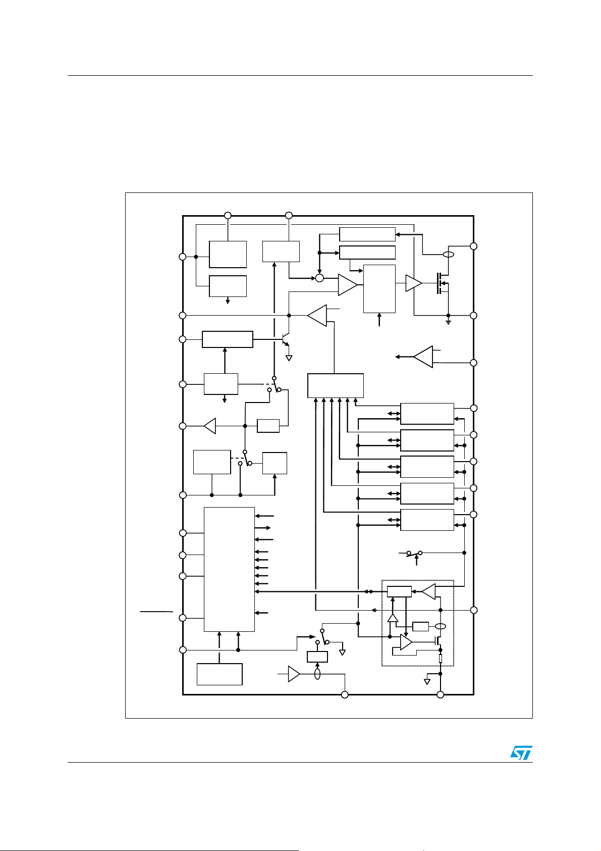
5 Operation description
The device can be divided into two sections: the boost section and the backlight driver
section. These sections are described in the next paragraphs. Figure 3 provides an
overview of the internal blocks of the device.
Figure 3. Simplified block diagram
VIN
LDO5
LDO5
COMP
COMP
BILIM
BILIM
SS
SS
SYNC
SYNC
FSW
FSW
AVCC
AVCC
EN
EN
MODE
MODE
FAULT
FAULT
DIM
DIM
VIN
+5V
+5V
LDO
LDO
UVLO
UVLO
Detector
Detector
UVLO
UVLO
Current Limit
Current Limit
Soft Start
Soft Start
Prot_EN
Prot_EN
Ext Sync
Ext Sync
Detector
Detector
CONTROL
CONTROL
LOGIC
LOGIC
Thermal
Thermal
Shutdown
Shutdown
SLOPE
SLOPE
Ramp
Ramp
Generator
Generator
÷2
÷2
OSC
OSC
Prot_EN
Prot_EN
Boost_EN
Boost_EN
UVLO
UVLO
CTRL6
CTRL6
CTRL5
CTRL5
CTRL4
CTRL4
CTRL3
CTRL3
CTRL2
CTRL2
OVP
OVP
1.2V
1.2V
+
+
+
+
+
+
g
m
g
m
_
_
Min Voltage
Min Voltage
Selector
Selector
CTRL1
CTRL1
ROW1
ROW1
V
V
I to V
I to V
Current Sense
Current Sense
ZCD
ZCD
+
+
Boost
Boost
Control
Control
_
_
Logic
Logic
0.7V
0.7V
Boost_EN
Boost_EN
CTRL6
CTRL6
CTRL5
CTRL5
CTRL4
CTRL4
CTRL3
CTRL3
CTRL2
CTRL2
OVP
OVP
V
ROW6
V
ROW6
V
ROW5
V
ROW5
V
ROW4
V
ROW4
V
ROW3
V
ROW3
V
ROW2
V
ROW2
4V
4V
LOGIC
LOGIC
Current
Current
Generator 1
Generator 1
Current
Current
Generator 6
Generator 6
Current
Current
Generator 5
Generator 5
Current
Current
Generator 4
Generator 4
Current
Current
Generator 3
Generator 3
Current
Current
Generator 2
Generator 2
MODE
MODE
I to V
I to V
+
+
_
_
_
_
+
+_+
V
V
TH,FLT
TH,FLT
1.172V
1.172V
LX
LX
PGND
PGND
OVSEL
OVSEL
ROW6
ROW6
ROW5
ROW5
ROW4
ROW4
ROW3
ROW3
ROW2
ROW2
ROW1
ROW1
10/46
RILIM
RILIM
SGND
SGND
AM00596v1
LED7706 Operation description
5.1 Boost section
5.1.1 Functional description
The LED7706 is a monolithic LEDs driver for the backlight of LCD panels and it consists of a
boost converter and six PWM-dimmable current generators.
The boost section is based on a constant switching frequency, peak current-mode
architecture. The boost output voltage is controlled such that the lowest row's voltage,
referred to SGND, is equal to an internal reference voltage (400 mV typ. see Figure 5). The
input voltage range is from 4.5 V up to 36 V. In addition, the LED7706 has an internal LDO
that supplies the internal circuitry of the device and is capable to deliver up to 40 mA. The
input of the LDO is the VIN pin.
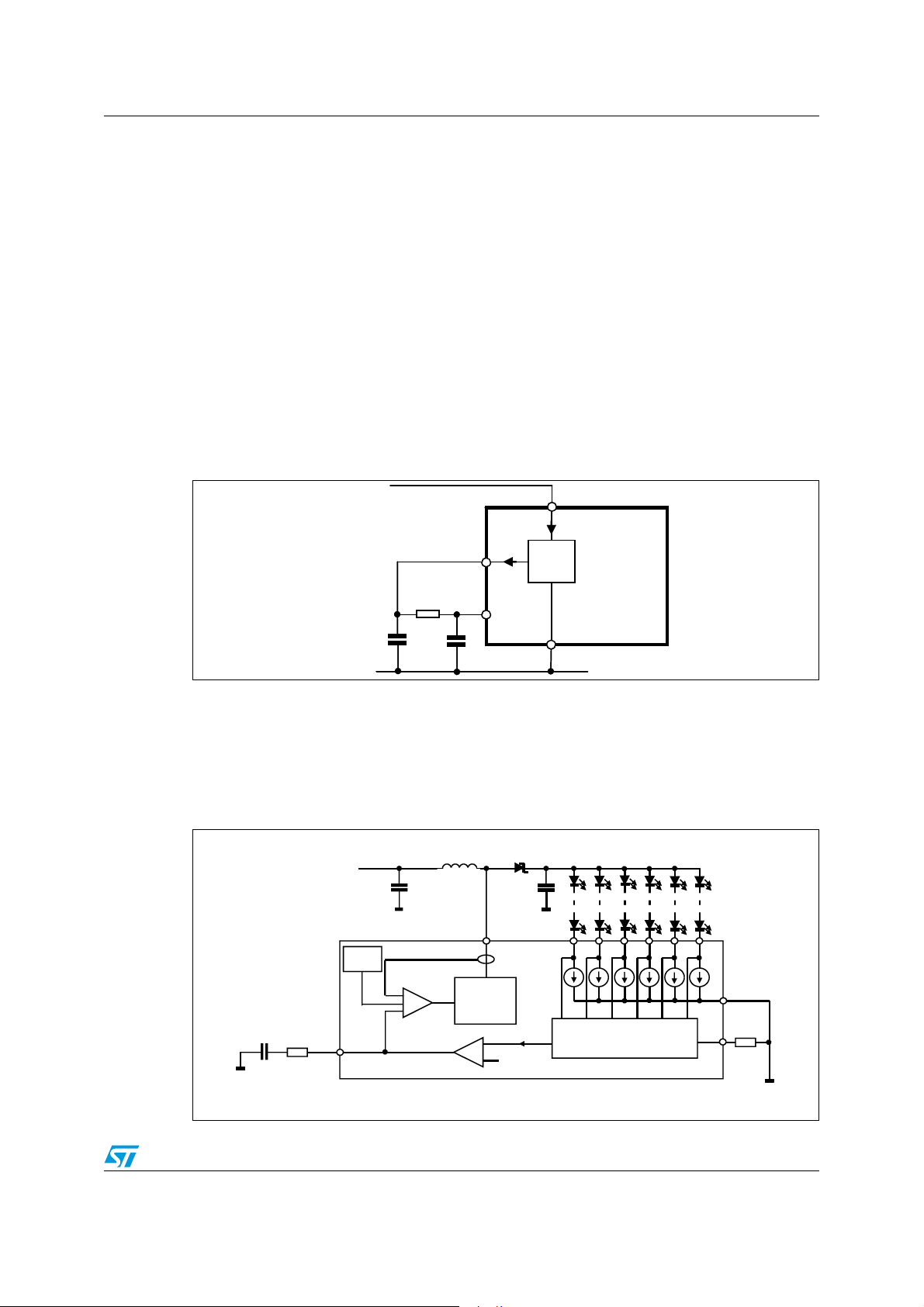
The LDO5 pin is the LDO output and the supply for the power MOSFET driver at the same
time. The AVCC pin is the supply for the analog circuitry and should be connected to the
LDO output through a simple RC filter in order to improve the noise rejection.
Figure 4. AVCC filtering
VIN
VIN
LDO5
CLDO5
CLDO5
1uF
1uF
Rfilt
Rfilt
4R7
4R7
C
C
AVCC
AVCC
100nF
100nF
LDO5
AVCC
AVCC
LDO
LDO
SGND
SGND
LED7706
LED7706
AM00597v1
Two loops are involved in regulating the current sunk by the generators.
The main loop is related to the boost regulator and uses a constant frequency peak currentmode architecture to regulate the power rail that supplies the LEDs (Figure 5), while an
internal current loop regulates the same current (flowing through the LEDs) at each row
according to the set value (RILIM pin).
Figure 5. Main loop and current loop diagram
V
IN
LX
Slope
PWM
ROWx
SGND
COMP
RILIM
E/A
Error amplifier
Minimum voltage drop
selector
0.4V
11/46
AM00598v1
Operation description LED7706
A dedicated circuit automatically selects the lowest voltage drop among all the rows and
provides this voltage to the main loop that, in turn, regulates the output voltage. In fact, once
the reference generator has been detected, the error amplifier compares its voltage drop to
the internal reference voltage and varies the COMP output. The voltage at the COMP pin
determines the inductor peak current at each switching cycle. The output voltage of the
boost regulator is thus determined by the total forward voltage of the LEDs strings (see
Figure 6):
Equation 1
m
N
OUT
ROWS
=
1i
LEDS
Σ
=
mV400)V(maxV
+=
j,F
1j
where the first term represents the highest total forward voltage drop over N active rows and
the second is the voltage drop across the leading generator (400 mV typ.).
The device continues to monitor the voltage drop across all the rows and automatically
switches to the current generator having the lowest voltage drop.
Figure 6. Calculation of the output voltage of the boost regulator
Row with the highest voltage
V
IN
drop across LEDs
5.1.2 Enable function
The LED7706 is enabled by the EN pin. This pin is active high and, when forced to SGND,
the device is turned off. This pin is connected to a permanently active 2.5 μA current source;
when sudden device turn-on at power-up is required, this pin must be left floating or
connected to a delay capacitor. When turned off, the LED7706 quickly discharges the
soft-start capacitor and turns off the power MOSFET, the current generators and the LDO.
The power consumption is thus reduced to 20 μA only.
In applications where the dimming signal is used to turn on and off the device, the EN pin
can be connected to the DIM pin as shown in Figure 7.
Boost
controller
Current
generators
section
I
LED
400 mV
generator
max
Σ
Leading
V
F
V
BOOST
AM00599v1
12/46
LED7706 Operation description
Figure 7. Enable pin driven by dimming signal
DIM
DIM
BAS69
BAS69
EN
220kΩ
220kΩ
100nF
100nF
EN
LED7706
LED7706
SGND
SGND
AM00600v1
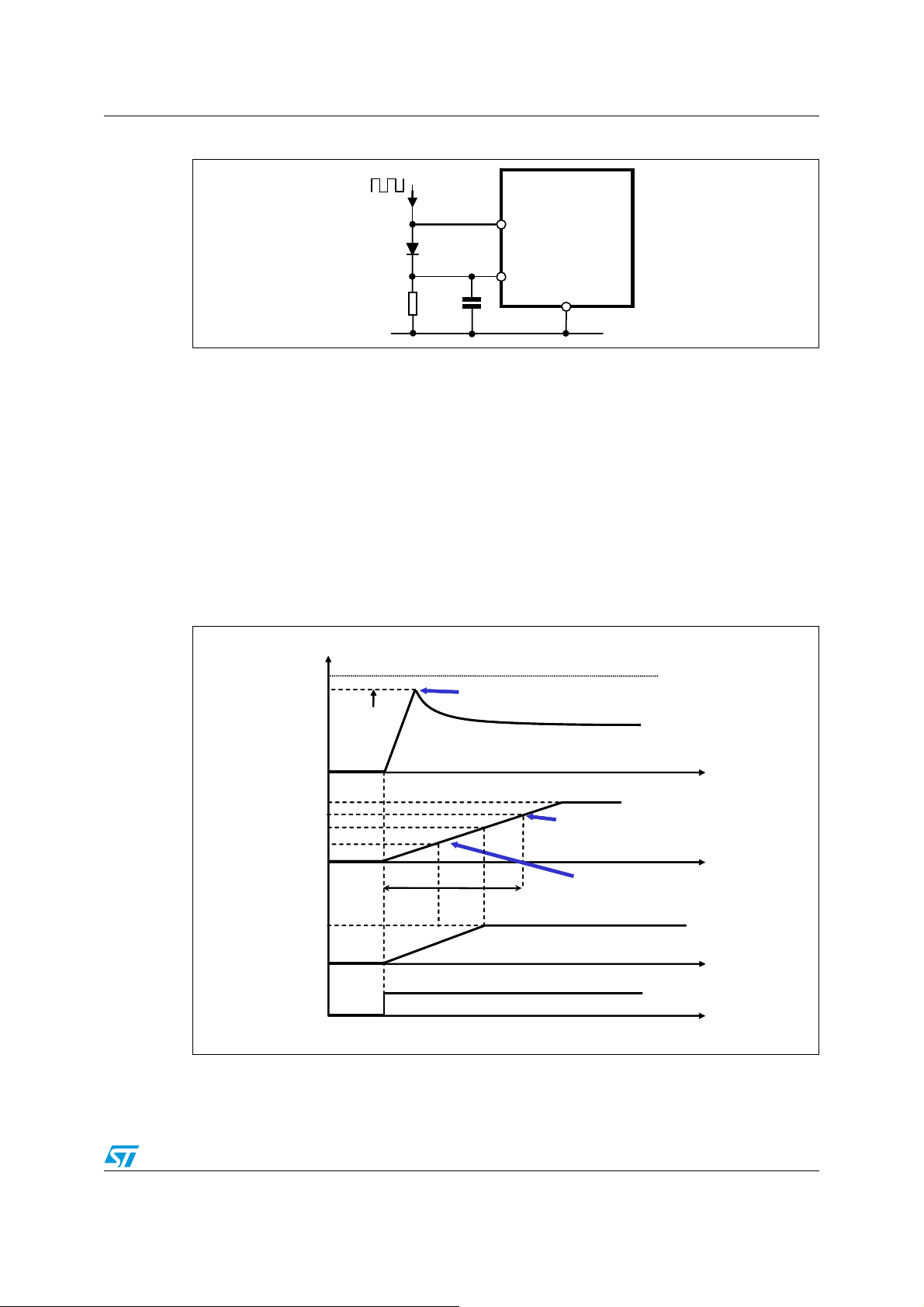
5.1.3 Soft-start
The soft-start function is required to perform a correct start-up of the system, controlling the
inrush current required to charge the output capacitor and to avoid output voltage overshoot.
The soft-start duration is set connecting an external capacitor between the SS pin and
ground. This capacitor is charged with a 5 μA (typ.) constant current, forcing the voltage on
the SS pin to ramp up. When this voltage increases from zero to nearly 1.2 V, the current
limit of the power MOSFET is proportionally released from zero to its final value. However,
because of the limited minimum on-time of the switching section, the inductor might saturate
due to current runaway. To solve this problem the switching frequency is reduced to one half
of the nominal value at the beginning of the soft-start phase. The nominal switching
frequency is restored after the SS pin voltage has crossed 0.8 V.
Figure 8. Soft-start sequence waveforms in case of floating rows
OVP
OVP
Floating ROWs detection
Floating ROWs detection
95% of
95% of
OVP
AVCC
AVCC
2.4V
2.4V
1.2V
1.2V
0.8V
0.8V
100%
100%
OVP
t
ss
t
ss
Current limit
Current limit
Output voltage
Output voltage
SS pin voltage
SS pin voltage
Protections turn active
Protections turn active
Nominal switching
Nominal switching
frequency release
frequency release
EN pin voltage
EN pin voltage
t
t
AM00601v1
During the soft-start phase the floating rows detection is also performed. In presence of one
or more floating rows, the voltage across the involved current generator drops to zero. This
voltage becomes the inverting input of the error amplifier through the minimum voltage drop
13/46

Operation description LED7706
selector (see Figure 5). As a consequence the error amplifier is unbalanced and the loop
reacts by increasing the output voltage. When it reaches the floating row detection (FRD)
threshold (95% of the OVP threshold), the floating rows are managed according to
Section 5.3 on page 21). After the SS voltage reaches a 2.4 V threshold, the start-up
(see
finishes and all the protections turn active. The soft-start capacitor C
can be calculated
SS
Ta bl e 6
according to equation 2.
Equation 2
⋅
tI
≅
C
SS
SSSS
4.2
Where I
= 5 µA and tSS is the desired soft-start duration.
SS
5.1.4 Overvoltage protection
An adjustable over-voltage protection is available. It can be set feeding the OVSEL pin with a
partition of the output voltage. The voltage of the central tap of the divider is thus compared
to a fixed 1.234 V threshold. When the voltage on the OVSEL pin exceeds the OV threshold,
the FAULT pin is tied low and the device is turned off; this condition is latched and the
LED7706 is restarted
occurs when the LDO output falls below the lower UVLO threshold and subsequently
crosses the upper UVLO threshold during the rising phase of the input voltage). Normally,
the value of the high-side resistors of the divider must be chosen as high as possible (but
lower than 1 M
(during the off phase of the dimming cycle). The R2/R1 ratio is calculated to trigger the OVP
circuitry as soon as the output voltage is 2 V higher than the maximum value for a given LED
string (see equation 3). Two additional filtering capacitors, C
improve noise rejection at the OVSEL pin, as shown in
in the 100 pF-330 pF range, while the C
Equation 3
by toggling the EN pin or by performing a Power-On Reset (the POR
Ω) to reduce the output capacitor discharge when the boost converter is off
Figure 9. The typical value for C10 is
13 value is given by equation 4.
RR
⋅=
12
OVP,OUT
V234.1
−+
10 and C13, may be required to
)V234.1V2V(
Equation 4
14/46
R
2
C2C ⋅=
1013
R
1
 Loading...