

Page 1
3 A monolithic step-down current source with synchronous
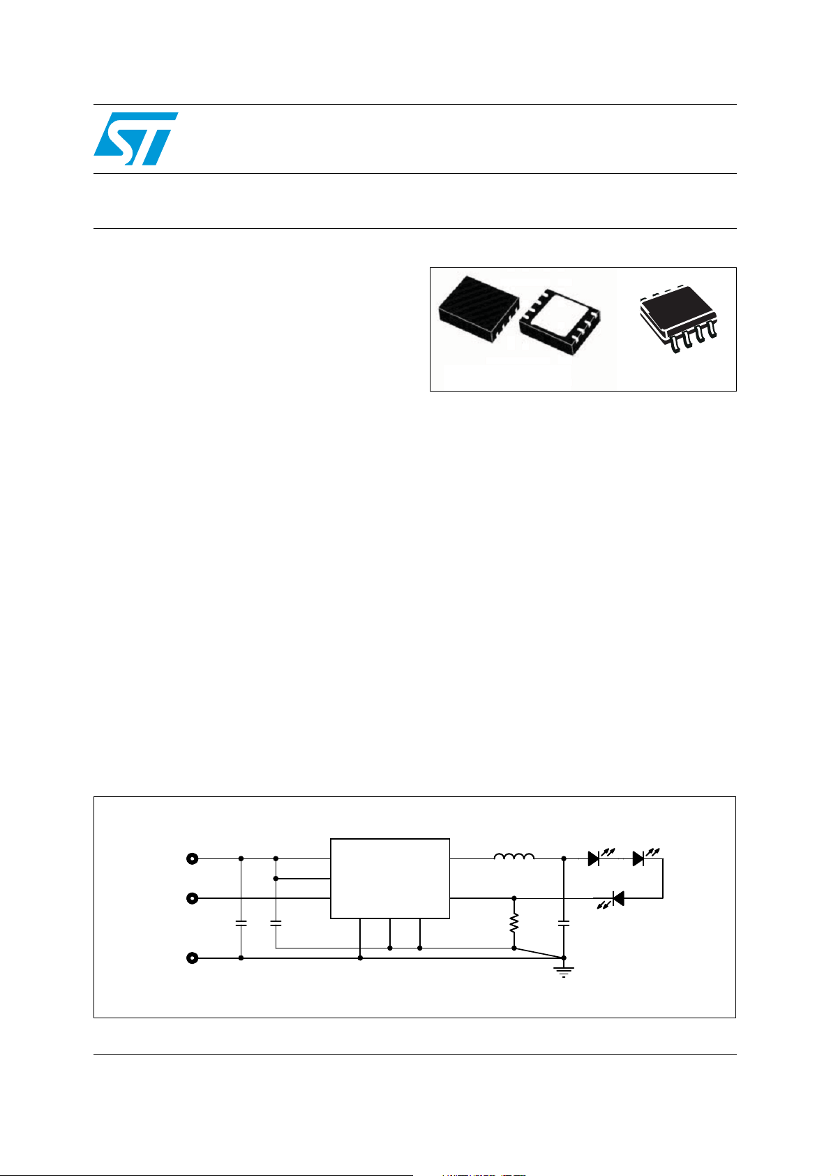
VFQFPN8 4x4
SO8
!-V
Features
■ 3.0 V to 18 V operating input voltage range
■ 850 kHz fixed switching frequency
■ 100 mV typ. current sense voltage drop
■ PWM dimming
■ ± 7% output current accuracy
■ Synchronous rectification
■ 95 mΩ HS / 69 mΩ LS typical R
■
Peak current mode architecture
■ Embedded compensation network
■ Internal current limiting
■ Ceramic output capacitor compliant
■ Thermal shutdown
Applications
■ High brightness LED driving
■ Halogen bulb replacement
■ General lighting
■ Signage
DS(on)
LED2000
rectification
Datasheet — production data
Description
The LED2000 is an 850 kHz fixed switching
frequency monolithic step-down DC-DC converter
designed to operate as precise constant current
source with an adjustable current capability up to
3 A DC. The embedded PWM dimming circuitry
features LED brightness control. The regulated
output current is set connecting a sensing resistor
to the feedback pin. The embedded synchronous
rectification and the 100 mV typical R
voltage drop enhance the efficiency performance.
The size of the overall application is minimized
thanks to the high switching frequency and
ceramic output capacitor compatibility. The device
is fully protected against thermal overheating,
overcurrent and output short-circuit.
SENSE
The LED2000 is available in VFQFPN 4 mm x 4
mm 8-lead package, and standard SO8.
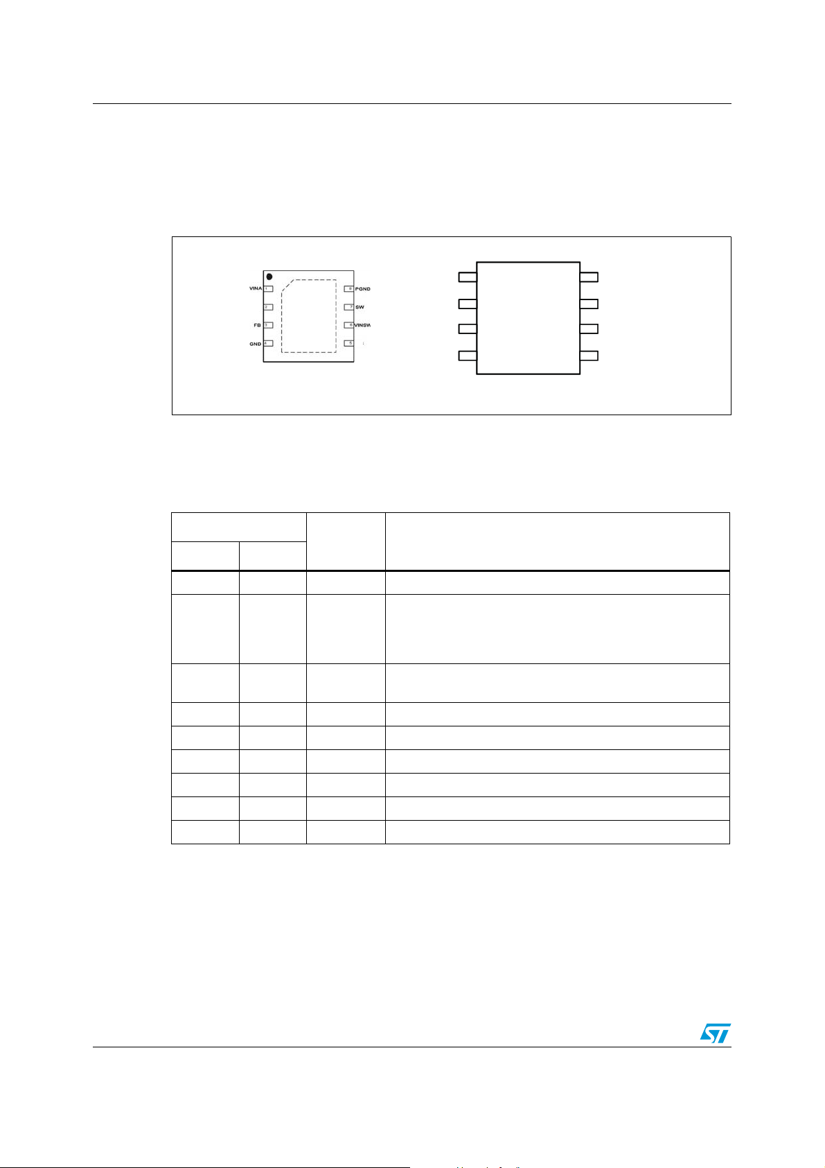
Figure 1. Typical application circuit
,%$,%$
6).6).
$)-$)-
'.$'.$
#).#). #&,4#&,4
6).?37
6).?!
$)-
0'.$
!'.$
%0
37
&"
July 2012 Doc ID 023432 Rev 2 1/39
This is information on a product in full production.
,,
2323 #/54#/54
www.st.com
39
Page 2

Contents LED2000
Contents
1 Pin settings . . . . . . . . . . . . . . . . . . . . . . . . . . . . . . . . . . . . . . . . . . . . . . . . 6
1.1 Pin connection . . . . . . . . . . . . . . . . . . . . . . . . . . . . . . . . . . . . . . . . . . . . . . 6
1.2 Pin description . . . . . . . . . . . . . . . . . . . . . . . . . . . . . . . . . . . . . . . . . . . . . . 6
2 Maximum ratings . . . . . . . . . . . . . . . . . . . . . . . . . . . . . . . . . . . . . . . . . . . . 7
3 Thermal data . . . . . . . . . . . . . . . . . . . . . . . . . . . . . . . . . . . . . . . . . . . . . . . 7
4 Electrical characteristics . . . . . . . . . . . . . . . . . . . . . . . . . . . . . . . . . . . . . 8
5 Functional description . . . . . . . . . . . . . . . . . . . . . . . . . . . . . . . . . . . . . . . 9
5.1 Power supply and voltage reference . . . . . . . . . . . . . . . . . . . . . . . . . . . . . 9
5.2 Voltage monitor . . . . . . . . . . . . . . . . . . . . . . . . . . . . . . . . . . . . . . . . . . . . 10
5.3 Soft-start . . . . . . . . . . . . . . . . . . . . . . . . . . . . . . . . . . . . . . . . . . . . . . . . . . 10
5.4 Error amplifier . . . . . . . . . . . . . . . . . . . . . . . . . . . . . . . . . . . . . . . . . . . . . . 10
5.5 Thermal shutdown . . . . . . . . . . . . . . . . . . . . . . . . . . . . . . . . . . . . . . . . . . 11
6 Application notes . . . . . . . . . . . . . . . . . . . . . . . . . . . . . . . . . . . . . . . . . . 12
6.1 Closing the loop . . . . . . . . . . . . . . . . . . . . . . . . . . . . . . . . . . . . . . . . . . . . 12
6.2 G
6.3 Error amplifier compensation network . . . . . . . . . . . . . . . . . . . . . . . . . . . 13
6.4 LED small signal model . . . . . . . . . . . . . . . . . . . . . . . . . . . . . . . . . . . . . . 15
6.5 Total loop gain . . . . . . . . . . . . . . . . . . . . . . . . . . . . . . . . . . . . . . . . . . . . . 17
6.6 Dimming operation . . . . . . . . . . . . . . . . . . . . . . . . . . . . . . . . . . . . . . . . . . 18
6.7 eDesign studio software . . . . . . . . . . . . . . . . . . . . . . . . . . . . . . . . . . . . . . 21
(s) control to output transfer function . . . . . . . . . . . . . . . . . . . . . . . . . 12
CO
6.5.1 Example . . . . . . . . . . . . . . . . . . . . . . . . . . . . . . . . . . . . . . . . . . . . . . . . . 17
6.6.1 Dimming frequency vs. dimming depth . . . . . . . . . . . . . . . . . . . . . . . . . 20
7 Application information . . . . . . . . . . . . . . . . . . . . . . . . . . . . . . . . . . . . . 22
7.1 Component selection . . . . . . . . . . . . . . . . . . . . . . . . . . . . . . . . . . . . . . . . 22
7.1.1 Sensing resistor . . . . . . . . . . . . . . . . . . . . . . . . . . . . . . . . . . . . . . . . . . . 22
7.1.2 Inductor and output capacitor selection . . . . . . . . . . . . . . . . . . . . . . . . . 22
7.1.3 Input capacitor . . . . . . . . . . . . . . . . . . . . . . . . . . . . . . . . . . . . . . . . . . . . 24
2/39 Doc ID 023432 Rev 2
Page 3

LED2000 Contents
7.2 Layout considerations . . . . . . . . . . . . . . . . . . . . . . . . . . . . . . . . . . . . . . . . 26
7.3 Thermal considerations . . . . . . . . . . . . . . . . . . . . . . . . . . . . . . . . . . . . . . 27
7.4 Short-circuit protection . . . . . . . . . . . . . . . . . . . . . . . . . . . . . . . . . . . . . . . 28
7.5 Application circuit . . . . . . . . . . . . . . . . . . . . . . . . . . . . . . . . . . . . . . . . . . . 30
8 Typical characteristics . . . . . . . . . . . . . . . . . . . . . . . . . . . . . . . . . . . . . . 33
9 Ordering information . . . . . . . . . . . . . . . . . . . . . . . . . . . . . . . . . . . . . . . 34
10 Package mechanical data . . . . . . . . . . . . . . . . . . . . . . . . . . . . . . . . . . . . 35
11 Revision history . . . . . . . . . . . . . . . . . . . . . . . . . . . . . . . . . . . . . . . . . . . 38
Doc ID 023432 Rev 2 3/39
Page 4

List of tables LED2000
List of tables
Table 1. Pin description . . . . . . . . . . . . . . . . . . . . . . . . . . . . . . . . . . . . . . . . . . . . . . . . . . . . . . . . . . . 6
Table 2. Absolute maximum ratings . . . . . . . . . . . . . . . . . . . . . . . . . . . . . . . . . . . . . . . . . . . . . . . . . . 7
Table 3. Thermal data. . . . . . . . . . . . . . . . . . . . . . . . . . . . . . . . . . . . . . . . . . . . . . . . . . . . . . . . . . . . . 7
Table 4. Electrical characteristics . . . . . . . . . . . . . . . . . . . . . . . . . . . . . . . . . . . . . . . . . . . . . . . . . . . . 8
Table 5. Uncompensated error amplifier characteristics. . . . . . . . . . . . . . . . . . . . . . . . . . . . . . . . . . 10
Table 6. Inductor selection . . . . . . . . . . . . . . . . . . . . . . . . . . . . . . . . . . . . . . . . . . . . . . . . . . . . . . . . 24
Table 7. List of ceramic capacitors for the LED2000 . . . . . . . . . . . . . . . . . . . . . . . . . . . . . . . . . . . . 25
Table 8. Component list . . . . . . . . . . . . . . . . . . . . . . . . . . . . . . . . . . . . . . . . . . . . . . . . . . . . . . . . . . 31
Table 9. Ordering information . . . . . . . . . . . . . . . . . . . . . . . . . . . . . . . . . . . . . . . . . . . . . . . . . . . . . . 34
Table 10. VFQFPN8 (4x4x1.08 mm) mechanical data . . . . . . . . . . . . . . . . . . . . . . . . . . . . . . . . . . . . 35
Table 11. SO-8 mechanical data . . . . . . . . . . . . . . . . . . . . . . . . . . . . . . . . . . . . . . . . . . . . . . . . . . . . 36
Table 12. Document revision history . . . . . . . . . . . . . . . . . . . . . . . . . . . . . . . . . . . . . . . . . . . . . . . . . 38
4/39 Doc ID 023432 Rev 2
Page 5

LED2000 List of figures
List of figures
Figure 1. Typical application circuit . . . . . . . . . . . . . . . . . . . . . . . . . . . . . . . . . . . . . . . . . . . . . . . . . . . 1
Figure 2. Pin connection (top view) . . . . . . . . . . . . . . . . . . . . . . . . . . . . . . . . . . . . . . . . . . . . . . . . . . . 6
Figure 3. LED2000 block diagram . . . . . . . . . . . . . . . . . . . . . . . . . . . . . . . . . . . . . . . . . . . . . . . . . . . . 9
Figure 4. Internal circuit . . . . . . . . . . . . . . . . . . . . . . . . . . . . . . . . . . . . . . . . . . . . . . . . . . . . . . . . . . . 10
Figure 5. Block diagram of the loop . . . . . . . . . . . . . . . . . . . . . . . . . . . . . . . . . . . . . . . . . . . . . . . . . . 12
Figure 6. Transconductance embedded error amplifier . . . . . . . . . . . . . . . . . . . . . . . . . . . . . . . . . . . 14
Figure 7. Equivalent series resistor . . . . . . . . . . . . . . . . . . . . . . . . . . . . . . . . . . . . . . . . . . . . . . . . . . 16
Figure 8. Load equivalent circuit . . . . . . . . . . . . . . . . . . . . . . . . . . . . . . . . . . . . . . . . . . . . . . . . . . . . 16
Figure 9. Module plot . . . . . . . . . . . . . . . . . . . . . . . . . . . . . . . . . . . . . . . . . . . . . . . . . . . . . . . . . . . . . 18
Figure 10. Phase plot . . . . . . . . . . . . . . . . . . . . . . . . . . . . . . . . . . . . . . . . . . . . . . . . . . . . . . . . . . . . . . 18
Figure 11. Dimming operation example . . . . . . . . . . . . . . . . . . . . . . . . . . . . . . . . . . . . . . . . . . . . . . . . 19
Figure 12. LED current falling edge operation . . . . . . . . . . . . . . . . . . . . . . . . . . . . . . . . . . . . . . . . . . . 20
Figure 13. Dimming signal . . . . . . . . . . . . . . . . . . . . . . . . . . . . . . . . . . . . . . . . . . . . . . . . . . . . . . . . . . 21
Figure 14. eDesign studio screenshot . . . . . . . . . . . . . . . . . . . . . . . . . . . . . . . . . . . . . . . . . . . . . . . . . 21
Figure 15. Equivalent circuit. . . . . . . . . . . . . . . . . . . . . . . . . . . . . . . . . . . . . . . . . . . . . . . . . . . . . . . . . 23
Figure 16. Layout example . . . . . . . . . . . . . . . . . . . . . . . . . . . . . . . . . . . . . . . . . . . . . . . . . . . . . . . . . 26
Figure 17. Switching losses . . . . . . . . . . . . . . . . . . . . . . . . . . . . . . . . . . . . . . . . . . . . . . . . . . . . . . . . . 27
Figure 18. Constant current protection triggering Hiccup mode . . . . . . . . . . . . . . . . . . . . . . . . . . . . . 30
Figure 19. Demonstration board application circuit . . . . . . . . . . . . . . . . . . . . . . . . . . . . . . . . . . . . . . . 30
Figure 20. PCB layout (component side) . . . . . . . . . . . . . . . . . . . . . . . . . . . . . . . . . . . . . . . . . . . . . . . 31
Figure 21. PCB layout (bottom side) . . . . . . . . . . . . . . . . . . . . . . . . . . . . . . . . . . . . . . . . . . . . . . . . . . 32
Figure 22. Soft-start . . . . . . . . . . . . . . . . . . . . . . . . . . . . . . . . . . . . . . . . . . . . . . . . . . . . . . . . . . . . . . . 33
Figure 23. Load regulation . . . . . . . . . . . . . . . . . . . . . . . . . . . . . . . . . . . . . . . . . . . . . . . . . . . . . . . . . . 33
Figure 24. Dimming operation . . . . . . . . . . . . . . . . . . . . . . . . . . . . . . . . . . . . . . . . . . . . . . . . . . . . . . . 33
Figure 25. LED current rising edge . . . . . . . . . . . . . . . . . . . . . . . . . . . . . . . . . . . . . . . . . . . . . . . . . . . 33
Figure 26. LED current falling edge . . . . . . . . . . . . . . . . . . . . . . . . . . . . . . . . . . . . . . . . . . . . . . . . . . . 33
Figure 27. Hiccup current protection . . . . . . . . . . . . . . . . . . . . . . . . . . . . . . . . . . . . . . . . . . . . . . . . . . 33
Figure 28. Efficiency vs. IOUT (VIN 32 V) . . . . . . . . . . . . . . . . . . . . . . . . . . . . . . . . . . . . . . . . . . . . . . 34
Figure 29. Thermal shutdown protection . . . . . . . . . . . . . . . . . . . . . . . . . . . . . . . . . . . . . . . . . . . . . . . 34
Figure 30. VFQFPN8 (4x4x1.08 mm) package dimensions. . . . . . . . . . . . . . . . . . . . . . . . . . . . . . . . . 36
Figure 31. SO8 package dimensions. . . . . . . . . . . . . . . . . . . . . . . . . . . . . . . . . . . . . . . . . . . . . . . . . . 37
Doc ID 023432 Rev 2 5/39
Page 6
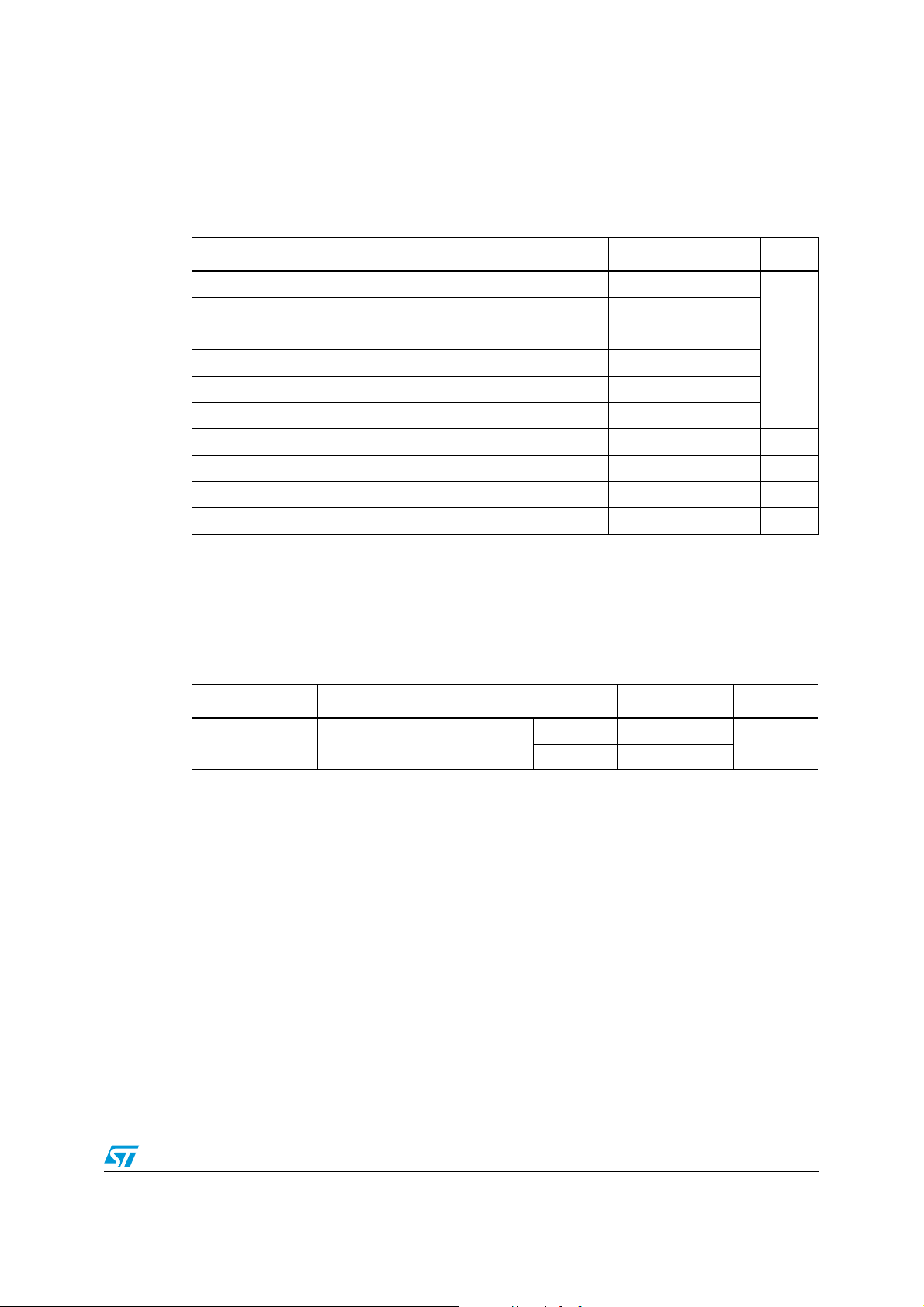
Pin settings LED2000
1
45
8
SW
PGND
VINA
VINSW
GND
AGND
FB
NC
VFQFPN
SO8 -BW
DIM
DIM
AM12893v1
1 Pin settings
1.1 Pin connection
Figure 2. Pin connection (top view)
1.2 Pin description
Table 1. Pin description
Package/pin
Type Description
VFQFPN S08-BW
13VINAAnalog circuitry power supply connection
Dimming control input. Logic low prevents the switching
24DIM
35FB
4 6 AGND Analog circuitry ground connection
5 - NC Not connected
68VIN
7 1 SW Regulator switching pin
8 2 PGND Power ground
- 7 GND Connect to AGND
activity, logic high enables it. A square wave on this pin
implements LED current PWM dimming. Connect to VIN
not used (see Section 6.6)
Feedback input. Connect a proper sensing resistor to set the
LED current
Power input voltage
SW
if
A
6/39 Doc ID 023432 Rev 2
Page 7
LED2000 Maximum ratings
2 Maximum ratings
Table 2. Absolute maximum ratings
Symbol Parameter Value Unit
V
INSW
V
INA
V
DIM
V
SW
V
PG
V
FB
I
FB
P
TOT
T
OP
T
stg
3 Thermal data
Table 3. Thermal data
Symbol Parameter Value Unit
R
thJA
Maximum thermal resistance
junction-ambient
Power input voltage -0.3 to 20
Input voltage -0.3 to 20
Dimming voltage -0.3 to V
Output switching voltage -1 to V
Power Good -0.3 to V
INA
IN
V
IN
Feedback voltage -0.3 to 2.5
FB current -1 to +1 mA
Power dissipation at TA < 60 °C 2 W
Operating junction temperature range -40 to 125 °C
Storage temperature range -55 to 150 °C
VFQFPN 40
(1)
SO8-BW 65
°C/W
1. Package mounted on demonstration board.
Doc ID 023432 Rev 2 7/39
Page 8
Electrical characteristics LED2000
4 Electrical characteristics
TJ=25 °C, VCC=12 V, unless otherwise specified.
Table 4. Electrical characteristics
Value
Symbol Parameter Test conditions
Min. Typ. Max.
Unit
Operating input voltage
range
V
IN
Device ON level 2.6 2.75 2.9
Device OFF level 2.4 2.55 2.7
R
DSON
R
DSON
V
I
I
FB
LIM
FB
Feedback voltage
VFB pin bias current
High-side switch on-
-P
resistance
Low-side switch on-
-N
resistance
Maximum limiting current
Oscillator
F
SW
Switching frequency 0.7 0.85 1 MHz
D Duty cycle
DC characteristics
I
Q
Quiescent current 1.5 2.5 mA
Dimming
(1)
318
V
Tj=25 °C 90 97 104
mV
Tj=125 °C 90 100 110
(1)
=750 mA 95 mΩ
I
SW
600 nA
ISW=750 mA 69 mΩ
(2)
(2)
0 100 %
5A
Switching activity 1.2
V
DIM
DIM threshold voltage
Switching activity
prevented
I
DIM
DIM current 2 μA
Soft-start
T
SS
Soft-start duration 1 ms
Protection
Thermal shutdown 150
T
SHDN
1. Specifications referred to TJ from -40 to +125 °C. Specifications in the -40 to +125 °C temperature range
are assured by design, characterization and statistical correlation.
2. Guaranteed by design.
Hystereris 15
8/39 Doc ID 023432 Rev 2
0.4
V
°C
Page 9
LED2000 Functional description
WSNIVANIV
OSC
E/A
DRIVER
DRIVER
DMD
OTP
MOSFET
CONTROL
LOGIC
REGULATOR
DIMMING
I_ S ENSE
COMP
PWM
OCP
REF
0.1V
SOFT-START
Vsum
Vc
OCP
UVLO
Vdrv
_p
Vdrv
_n
I2V
R
SENSE
SW
GNDP
GNDADIMFB
AM12894v1
5 Functional description
The LED2000 is based on a “peak current mode” architecture with fixed frequency control.
As a consequence, the intersection between the error amplifier output and the sensed
inductor current generates the control signal to drive the power switch.
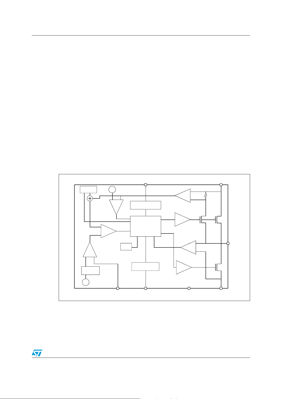
The main internal blocks shown in the block diagram in Figure 3 are:
● High-side and low-side embedded power element for synchronous rectification
● A fully integrated sawtooth oscillator with a typical frequency of 850 kHz
● A transconductance error amplifier
● An high-side current sense amplifier to track the inductor current
● A pulse width modulator (PWM) comparator and the circuitry necessary to drive the
internal power element
● The soft-start circuitry to decrease the inrush current at power-up
● The current limitation circuit based on the pulse-by-pulse current protection with
frequency divider
● The dimming circuitry for output current PWM
● The thermal protection function circuitry.
Figure 3. LED2000 block diagram
5.1 Power supply and voltage reference
The internal regulator circuit consists of a startup circuit, an internal voltage pre-regulator,
the BandGap voltage reference and the bias block that provides current to all the blocks.
The starter supplies the startup current to the entire device when the input voltage goes high
Doc ID 023432 Rev 2 9/39
Page 10
Functional description LED2000
STARTER
PREREGULATOR
IC BIAS
BANDGAP
VREF
VREG
Vcc
D00IN126
AM12895v1
and the device is enabled. The pre-regulator block supplies the BandGap cell with a preregulated voltage that has a very low supply voltage noise sensitivity.
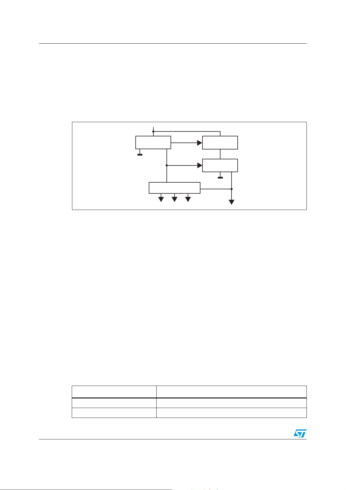
5.2 Voltage monitor
An internal block continuously senses the VCC, V
good, the regulator begins operating. There is also a hysteresis on the V
Figure 4. Internal circuit
5.3 Soft-start
The startup phase is implemented ramping the reference of the embedded error amplifier in
1 ms typ. time. It minimizes the inrush current and decreases the stress of the power
components at power-up.
During normal operation a new soft-start cycle takes place in case of:
● Thermal shutdown event
● UVLO event.
and Vbg. If the monitored voltages are
ref
(UVLO).
CC
The soft-start is disabled when DIM input goes high in order to maximize the dimming
performance.
5.4 Error amplifier
The voltage error amplifier is the core of the loop regulation. It is a transconductance
operational amplifier whose non-inverting input is connected to the internal voltage
reference (100 mV), while the inverting input (FB) is connected to the output current sensing
resistor.
The error amplifier is internally compensated to minimize the size of the final application.
Table 5. Uncompensated error amplifier characteristics
Description Value
Transconductance 250 µS
Low frequency gain 96 dB
10/39 Doc ID 023432 Rev 2
Page 11

LED2000 Functional description
Table 5. Uncompensated error amplifier characteristics (continued)
Description Value
C
C
R
C
The error amplifier output is compared with the inductor current sense information to
perform PWM control.
5.5 Thermal shutdown
The shutdown block generates a signal that disables the power stage if the temperature of
the chip goes higher than a fixed internal threshold (150 ± 10 °C typical). The sensing
element of the chip is close to the PDMOS area, ensuring fast and accurate temperature
detection. A 15 °C typical hysteresis prevents the device from turning ON and OFF
continuously during the protection operation.
195 pF
70 KΩ
Doc ID 023432 Rev 2 11/39
Page 12
Application notes LED2000
V
IN
-
+
-
LC filter
V
REF
error
amplifier
FB
compensation
network
PWM
comparator
HS
switch
R
S
L
C
OUT
R
C
C
C
+
PWM control
Current sense
LS
switch
V
OUT
V
CONTROL
GCO(s)
A
O
(s)
α
LED
GCOs()
R
0
R
i
-------
1
1
R
0TSW
⋅
L
---------------------------
m
C
1D–()0.5–⋅[]⋅+
-------------------------------------------------------- ------------------------------------------
1
s
ω
z
-----+
⎝⎠
⎛⎞
1
s
ω
p
------+
⎝⎠
⎛⎞
---------------------
F
H
s()⋅⋅⋅=
6 Application notes
6.1 Closing the loop
Figure 5. Block diagram of the loop
6.2 GCO(s) control to output transfer function
The accurate control to output transfer function for a buck peak current mode converter can
be written as:
Equation 1
where R
sense circuitry, ω
represents the load resistance, Ri the equivalent sensing resistor of the current
0
the single pole introduced by the LC filter and ωz the zero given by the
p
ESR of the output capacitor.
F
(s) accounts for the sampling effect performed by the PWM comparator on the output of
H
the error amplifier that introduces a double pole at one half of the switching frequency.
12/39 Doc ID 023432 Rev 2
Page 13

LED2000 Application notes
ω
Z
1
ESR C
OUT
⋅
------------------------------------=
ω
P
1
R
LOADCOUT
⋅
-------------------------------------------
m
C
1D–()0.5–⋅
LC
OUTfSW
⋅⋅
-------------------------------------------------+=
mC1
S
e
S
n
-------
+=
S
eVppfSW
⋅=
S
n
VINV
OUT
–
L
--------------------------------
R
i
⋅=
⎝
⎜
⎜
⎜
⎜
⎜
⎜
⎛
FHs()
1
1
s
ω
nQP
⋅
---------------------
s
2
ω
n
2
------++
--------------------------------------------=
ωnπ fSW⋅=
Q
P
1
π m
C
1D–()0.5–⋅[]⋅
------------------------------------------------------------ ----=
Equation 2
Equation 3
where:
Equation 4
represents the slope of the sensed inductor current, Se the slope of the external ramp
S
n
(V
peak-to-peak amplitude) that implements the slope compensation to avoid sub-
PP
harmonic oscillations at duty cycle over 50%.
The sampling effect contribution F
(s) is:
H
Equation 5
where:
Equation 6
and
Equation 7
6.3 Error amplifier compensation network
The LED2000 embeds (see Figure 6) the error amplifier and a pre-defined compensation
network which is effective in stabilizing the system in most application conditions.
Doc ID 023432 Rev 2 13/39
Page 14

Application notes LED2000
+
-
C
P
R
C
C
C
FB
COMP
dV
R
0
GmdV
V
+
E/A
R
C
C
C
C
P
C
0
AM12897v1
A0s()
A
V0
1s+ RcC
c
⋅⋅()⋅
s
2
R0C0Cp+()RcCcsR0Cc⋅ R0C0Cp+()RcCc⋅+⋅+()1+⋅+⋅⋅ ⋅⋅
------------------------------------------------------- ---------------------------------------------------------------- ----------------------------------------------------- ----------------------------------------=
f
P LF
1
2 π R
0Cc
⋅⋅ ⋅
------------------------------------------=
f
P HF
1
2 π R
cC0Cp
+()⋅⋅ ⋅
-------------------------------------------------------------=
F
Z
1
2 π R
cCc
⋅⋅ ⋅
------------------------------------------=
Figure 6. Transconductance embedded error amplifier
R
and CC introduce a pole and a zero in the open loop gain. CP does not significantly affect
C
system stability but it is useful to reduce the noise at the output of the error amplifier.
The transfer function of the error amplifier and its compensation network is:
Equation 8
where A
The poles of this transfer function are (if C
= Gm · Ro.
vo
>> C0+CP):
C
Equation 9
Equation 10
whereas the zero is defined as:
Equation 11
14/39 Doc ID 023432 Rev 2
Page 15

LED2000 Application notes
fZ11 6 kHz,= f
P LF
34 Hz,=
r
LED
1.3Ω I
LED
350m A=
0.9Ω I
LED
700m A=
⎩
⎨
⎧
The embedded compensation network is RC=70 K, CC=195 pF while CP and CO can be
considered as negligible. The error amplifier output resistance is 240 MΩ,
so the relevant
singularities are:
Equation 12
6.4 LED small signal model
Once the system reaches the working condition, the LEDs composing the row are biased
and their equivalent circuit can be considered as a resistor for frequencies << 1 MHz.
The LED manufacturer typically provides the equivalent dynamic resistance of the LED
biased at different DC currents. This parameter is required to study the behavior of the
system in the small signal analysis.
For instance, the equivalent dynamic resistance of the Luxeon III Star from Lumiled
measured with different biasing current level is reported below:
Equation 13
If the LED datasheet does not report the equivalent resistor value, it can be simply derived
as the tangent to the diode I-V characteristic in the present working point (see Figure 7).
Doc ID 023432 Rev 2 15/39
Page 16

Application notes LED2000
1
0.1
1
2
3
[V]
4
[A]
working point
AM12898v1
VIN
Rd1
COUT
L
L
Rd2
Rs
Dled1
Rs
D1
D
COUT
VIN
L
Dled2
AM12899v1
Figure 7. Equivalent series resistor
Figure 8 shows the equivalent circuit of the LED constant current generator.
Figure 8. Load equivalent circuit
As a consequence, the LED equivalent circuit gives the α
(s) term correlating the output
LED
voltage with the high impedance FB input:
16/39 Doc ID 023432 Rev 2
Page 17

LED2000 Application notes
α
LEDnLED
()
R
SENSE
n
LEDrLEDRSENSE
+⋅
-----------------------------------------------------------------=
Gs() GCOs() A0s() α
LEDnLED
()⋅⋅=
R
S
100 mV
700 mA
---------------------
140 m Ω≅=
α
LEDnLED
()
R
SENSE
n
LEDrLEDRSENSE
+⋅
------------------------------------------------------- ----------=
140 m Ω
21.1Ω⋅ 140 mΩ+
--------------------------------------------------- 0.06==
Equation 14
6.5 Total loop gain
In summary, the open loop gain can be expressed as:
Equation 15
Example 1
Design specification:
V
=12 V, V
IN
FW_LED
The inductor and capacitor value are dimensioned in order to meet the I
specification (see Section 7.1.2 for output capacitor and inductor selection guidelines):
=3.5 V, n
LED
= 2, r
= 1.1 Ω, I
LED
= 700 mA, I
LED
LED RIPPLE
LED RIPPLE
= 2%
L=10
μ
H, C
=2.2 μF MLCC (negligible ESR)
OUT
Accordingly, with Section 7.1.1 the sensing resistor value is:
Equation 16
Equation 17
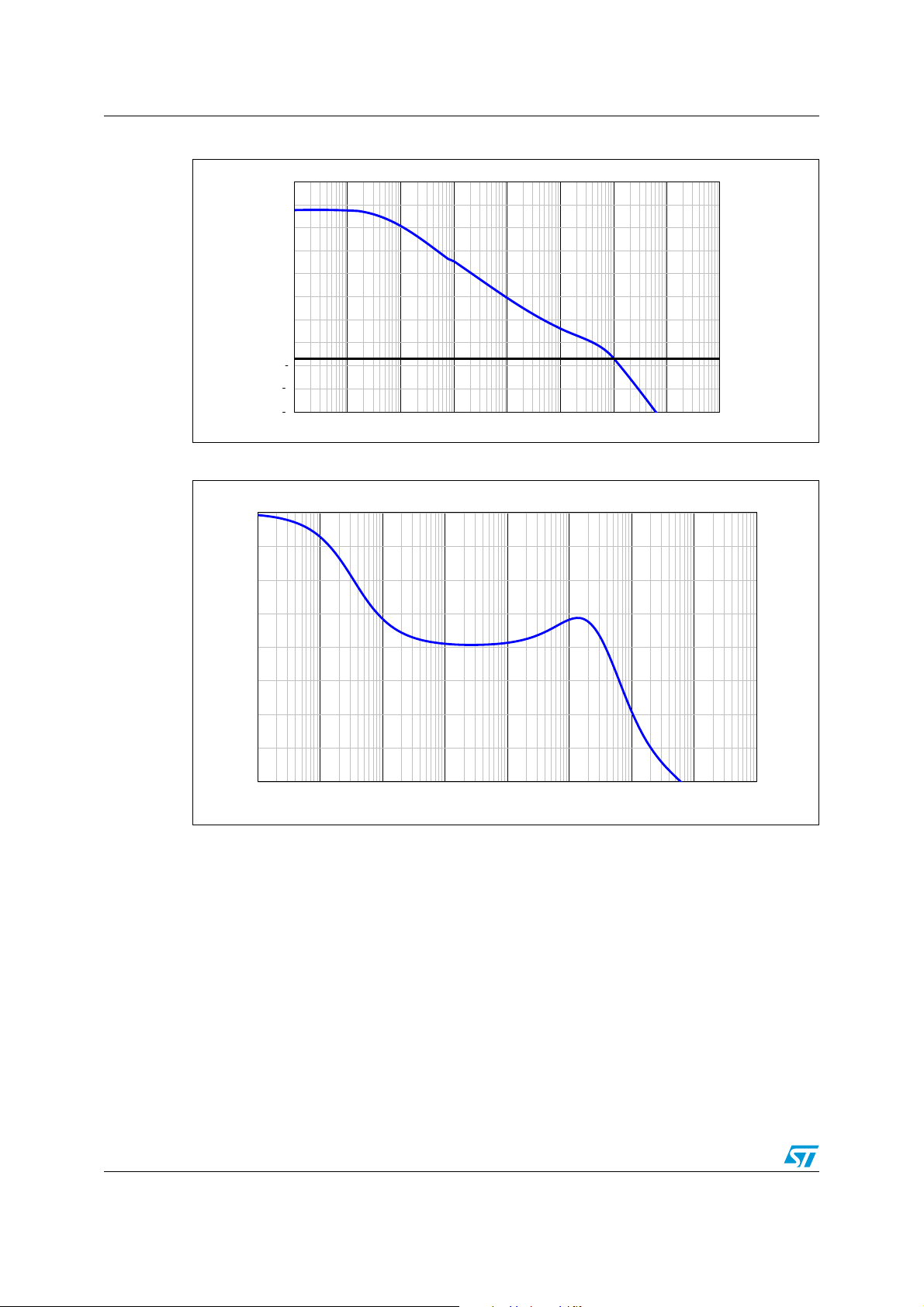
The gain and phase margin Bode diagrams are plotted respectively in Figure 9 and
Figure 10.
Doc ID 023432 Rev 2 17/39
Page 18
Application notes LED2000
%84%2.!,,//0-/$5,%
&REQUENCY;(Z=
-ODULE;D"=
!-V
%84%2.!,,//0'!).0(!3%
&REQUENCY;(Z=
0HASE
!-V
fC100 kHz= pm 47°=
Figure 9. Module plot
Figure 10. Phase plot
The cut-off frequency and the phase margin are:
Equation 18
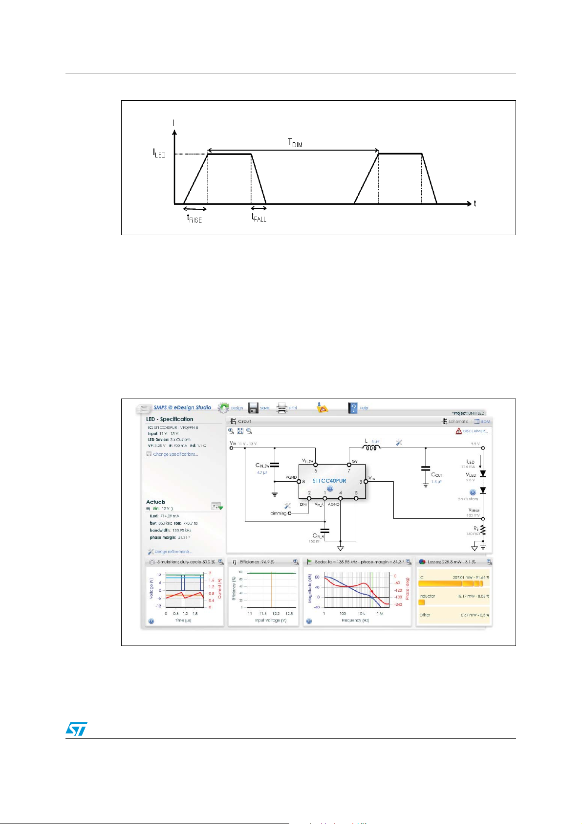
6.6 Dimming operation
The dimming input disables the switching activity, masking the PWM comparator output.
18/39 Doc ID 023432 Rev 2
The inductor current dynamic when dimming input goes high depends on the designed
system response. The best dimming performance is obtained maximizing the bandwidth
and phase margin, when it is possible.
As a general rule, the output capacitor minimization improves the dimming performance.
Page 19

LED2000 Application notes
AM12902v1
Figure 11. Dimming operation example
In fact, when dimming enables the switching activity, a small capacitor value is fast charged
with low inductor value. As a consequence, the LEDs current rising edge time is improved
and the inductor current oscillation reduced. An oversized output capacitor value requires
extra current for fast charge so generating certain inductor current oscillations
The switching activity is prevented as soon as the dimming signal goes low. Nevertheless,
the LED current drops to zero only when the voltage stored in the output capacitor goes
below a minimum voltage determined by the selected LEDs. As a consequence, a big
capacitor value makes the LED current falling time worse than a smaller one.
The LED2000 embeds dedicated circuitry to improve LED current falling time.
As soon as the dimming input goes low, the low-side is kept enabled to discharge C
OUT
until
the LED current drops to 60% of the nominal current. A negative current limitation (-1 A
typical) protects the device during this operation (see Figure 12).
Doc ID 023432 Rev 2 19/39
Page 20

Application notes LED2000
AM12903v1
rec gletan
T
RISETFALL
+
T
DIM
--------------------------------------------- 1«
→
trapezoid
T
RISETFALL
+
T
DIM
---------------------------------------------
1<
→
triangle
T
RISETFALL
+
T
DIM
--------------------------------------------- 1=
T
RISE
20μs≅
T
FALL
5μs≅
⎩
⎨
⎧
T
RISETFALL
+ 0.5 T
MIN_PULSE
⋅ 0.5 D
MINTDIMMING
⋅⋅==
Figure 12. LED current falling edge operation
6.6.1 Dimming frequency vs. dimming depth
As seen in Section 6.6, the LEDs current rising and falling edge time mainly depends on the
system bandwidth (T
The dimming performance depends on the minimum current pulse shape specification of
the final application. The ideal minimum current pulse has rectangular shape, however, it
degenerates into a trapezoid or, at worst, into a triangle, depending on the ratio (T
T
)/ T
FAL L
DIM
.
Equation 19
The small signal response in Figure 11 and Figure 12 is considered as an example.
Equation 20
Assuming the minimum current pulse shape specification as:
Equation 21:
) and the selected output capacitor value (T
RISE
RISE
and T
FAL L
).
RISE
+
it is possible to calculate the maximum dimming depth given the dimming frequency or vice
versa.
20/39 Doc ID 023432 Rev 2
Page 21
LED2000 Application notes
AM12904v1
AM12905v1
Figure 13. Dimming signal
For example, assuming a 1 kHz dimming frequency the maximum dimming depth is 5% or,
given a 2% dimming depth, it follows a 200 Hz maximum f
DIM
.
The LED2000 dimming performance is strictly dependent on the system small signal
response. As a consequence, an optimized compensation (good phase margin and
bandwidth maximized) and minimized C
value are crucial for the best performance.
OUT
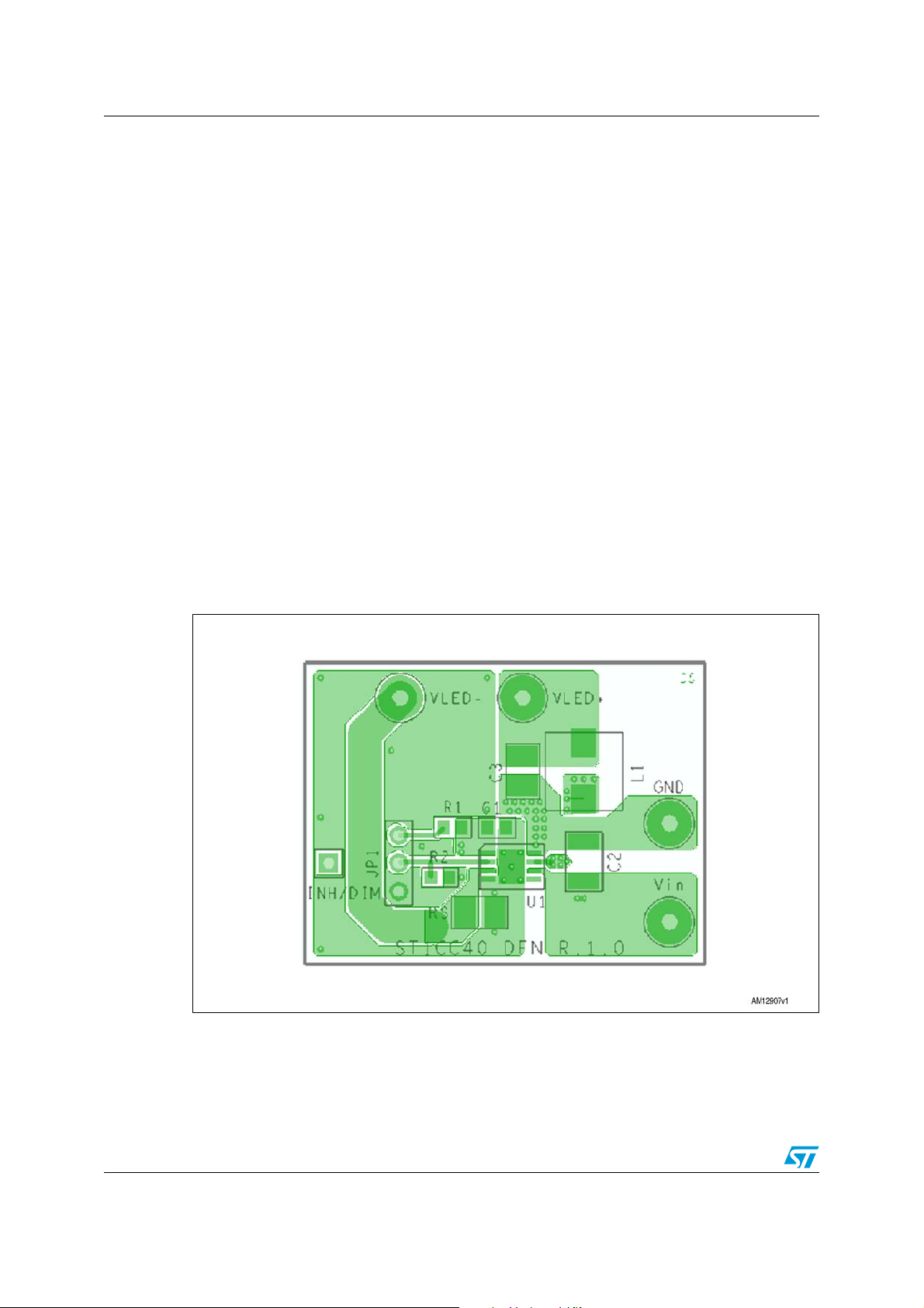
6.7 eDesign studio software
The LED2000 is supported by the eDesign software which can be viewed online at
www.st.com.
Figure 14. eDesign studio screenshot
The software easily supports the component sizing according to the technical information
given in this datasheet (see Section 6 and Section 7).
The end user is requested to fill in the requested information such as the input voltage
range, the selected LED parameters and the number of LEDs composing the row.
Doc ID 023432 Rev 2 21/39
Page 22

Application information LED2000
R
S
100 mV
I
LED
--------------------=
The software calculates external components according to the internal database. It is also
possible to define new components and ask the software to use them.
Bode plots, estimated efficiency and thermal performance are provided.
Finally, the user can save the design and print all the information including the bill of material
of the board.
7 Application information
7.1 Component selection
7.1.1 Sensing resistor
In closed loop operation the LED2000 feedback pin voltage is 100 mV, so the sensing
resistor calculation is expressed as:
Equation 22
Since the main loop (see Section 6.1) regulates the sensing resistor voltage drop, the
average current is regulated into the LEDs. The integration period is at minimum 5*T
since the system bandwidth can be dimensioned up to f
The system performs the output current regulation over a period which is at least five times
longer than the switching frequency. The output current regulation neglects the ripple
current contribution and its reliance on external parameters like input voltage and output
voltage variations (line transient and LED forward voltage spread). This performance can
not be achieved with simpler regulation loops such as a hysteretic control.
For the same reason, the switching frequency is constant over the application conditions,
which helps to tune the EMI filtering and to guarantee the maximum LED current ripple
specification in the application range. This performance can not be achieved using constant
ON/OFF-time architecture.
7.1.2 Inductor and output capacitor selection
The output capacitor filters the inductor current ripple that, given the application condition,
depends on the inductor value. As a consequence, the LED current ripple, that is the main
specification for a switching current source, depends on the inductor and output capacitor
selection.
/5 at maximum.
SW
SW
22/39 Doc ID 023432 Rev 2
Page 23

LED2000 Application information
$#2 $#2
#/54
2S
6).
,
%32
2D
6).
,,
%32
$LED
$$
#/54
$$
2S
2DN
$LEDN
!-V
I
RIPPLE
s()Δ
8
π
2
------
ΔI
L
1s ESRC
OUT
⋅⋅+()⋅⋅
1s R
S
ESR n
LEDRLED
⋅++()C
OUT
⋅⋅+
------------------------------------------------------------ ------------------------------------------------------------=
ΔI
L
V
OUT
L
----------------
T
OFF
⋅
n
LEDVFW_LED
100mV+⋅
L
-------------------------------------------------------------- ----------
T
OFF
⋅==
L
n
LEDVFW_LED
100mV+⋅
ΔI
L
---------------------------------------------------------- --------------
T
OFF
⋅
n
LEDVFW_LED
100mV+⋅
ΔI
L
-------------------------------------------------------- ----------------
1
n
LEDVFW_LED
100mV+⋅
V
IN
--------------------------------------------------------------- ---------–
⎝⎠
⎜⎟
⎛⎞
⋅==
ΔI
L
I
LED
------------
0.5≤
Figure 15. Equivalent circuit
The LED ripple current can be calculated as the inductor ripple current ratio flowing into the
output impedance using the Laplace transform (see Figure 11):
Equation 23
where the term 8/
a triangular shape) and
2
π
represents the main harmonic of the inductor current ripple (which has
ΔI
is the inductor current ripple.
L
Equation 24
so L value can be calculated as:
Equation 25
where T
is the OFF-time of the embedded high switch, given by 1-D.
OFF
As a consequence, the lower the inductor value (so the higher the current ripple), the higher
the C
value would be to meet the specification.
OUT
A general rule to dimension L value is:
Equation 26
Finally, the required output capacitor value can be calculated equalizing the LED current
ripple specification with the module of the Fourier transformer (see Equation 23) calculated
at f
frequency.
SW
Doc ID 023432 Rev 2 23/39
Page 24

Application information LED2000
I
RIPPLE
s=j ω⋅()Δ I
RIPPLE_SPEC
Δ=
ΔI
L
I
LED
------------ 0.5=
I
RMSIO
D
2D
2
⋅
η
------------------–
D
2
η
2
-------+⋅=
Equation 27
Example (see Section Example 1):
V
=12 V, I
IN
=700 mA, Δ
LED
ILED/ILED
=2%, V
FW_LED
=3.5 V, n
LED
=2.
A lower inductor value maximizes the inductor current slew rate for better dimming
performance. Equation 26 becomes:
Equation 28
which is satisfied selecting a10 μH inductor value.
The output capacitor value must be dimensioned according to Equation 27.
Finally, given the selected inductor value, a 2.2 μF ceramic capacitor value keeps the LED
current ripple ratio lower than the 2% of the nominal current. An output ceramic capacitor
type (negligible ESR) is suggested to minimize the ripple contribution given a fixed capacitor
value.
Table 6. Inductor selection
Manufacturer Series Inductor value (µH) Saturation current (A)
Wurth Elektronik
Coilcraft XPL 7030 2.2 to 10 29 to 7.2
7.1.3 Input capacitor
The input capacitor must be able to support the maximum input operating voltage and the
maximum RMS input current.
Since step-down converters draw current from the input in pulses, the input current is
squared and the height of each pulse is equal to the output current. The input capacitor
must absorb all this switching current, whose RMS value can be up to the load current
divided by two (worst case, with duty cycle of 50%). For this reason, the quality of these
capacitors must be very high to minimize the power dissipation generated by the internal
ESR, thereby improving system reliability and efficiency. The critical parameter is usually the
RMS current rating, which must be higher than the RMS current flowing through the
capacitor. The maximum RMS input current (flowing through the input capacitor) is:
Equation 29
WE-HCI 7040 1 to 4.7 20 to 7
WE-HCI 7050 4.9 to 10 20 to 4.0
where η is the expected system efficiency, D is the duty cycle and I
current. Considering η = 1 this function reaches its maximum value at D = 0.5 and the
24/39 Doc ID 023432 Rev 2
is the output DC
O
Page 25

LED2000 Application information
D
MAX
V
OUTVF
+
V
INMINVSW
–
---------------------------------------=
D
MIN
V
OUTVF
+
V
INMAXVSW
–
-----------------------------------------=
V
IN PP
I
O
CINfSW⋅
----------------------------
1
D
η
----–
⎝⎠
⎛⎞
D⋅
D
η
----
1D–()⋅+⋅=
equivalent RMS current is equal to IO divided by 2. The maximum and minimum duty cycles
are:
Equation 30
and
Equation 31
where V
internal PDMOS. Considering the range D
I
RMS
is the free-wheeling diode forward voltage and VSW the voltage drop across the
F
MIN
to D
, it is possible to determine the max.
MAX
going through the input capacitor. Capacitors that can be considered are:
Electrolytic capacitors:
These are widely used due to their low price and their availability in a wide range of
RMS current ratings.
The only drawback is that, considering ripple current rating requirements, they are
physically larger than other capacitors.
Ceramic capacitors:
If available for the required value and voltage rating, these capacitors usually have a
higher RMS current rating for a given physical dimension (due to very low ESR).
The drawback is the considerably high cost.
Tantalum capacitors:
Small tantalum capacitors with very low ESR are becoming more widely available.
However, they can occasionally burn if subjected to very high current during charge.
Therefore, it is suggested to avoid this type of capacitor for the input filter of the device
as they may be stressed by a high surge current when connected to the power supply.
Table 7. List of ceramic capacitors for the LED2000
Manufacturer Series
Capacitor value
(µC)
Rated voltage (V)
TAIYO YUDEN UMK325BJ106MM-T 10 50
MURATA GRM42-2 X7R 475K 50 4.7 50
If the selected capacitor is ceramic (so neglecting the ESR contribution), the input voltage
ripple can be calculated as:
Equation 32
Doc ID 023432 Rev 2 25/39
Page 26
Application information LED2000
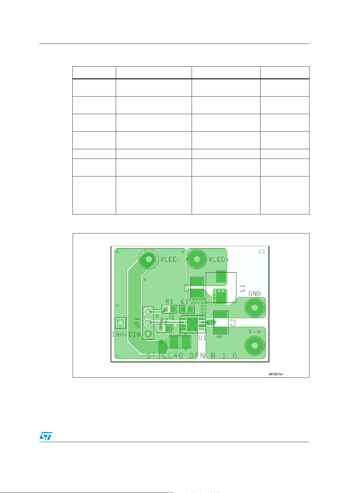
7.2 Layout considerations
The layout of switching DC-DC converters is very important to minimize noise and
interference. Power-generating portions of the layout are the main cause of noise and so
high switching current loop areas should be kept as small as possible and lead lengths as
short as possible.
High impedance paths (in particular the feedback connections) are susceptible to
interference, so they should be as far as possible from the high current paths. A layout
example is provided in Figure 16.
The input and output loops are minimized to avoid radiation and high frequency resonance
problems. The feedback pin to the sensing resistor path must be designed as short as
possible to avoid pick-up noise. Another important issue is the ground plane of the board. As
the package has an exposed pad, it is very important to connect it to an extended ground
plane in order to reduce the thermal resistance junction-to-ambient.
To increase the design noise immunity, different signal and power ground should be
implemented in the layout (see Section 7.5: Application circuit). The signal ground serves
the small signal components, the device analog ground pin, the exposed pad and a small
filtering capacitor connected to the VCC pin. The power ground serves the device ground
pin and the input filter. The different grounds are connected underneath the output
capacitor. Neglecting the current ripple contribution, the current flowing through this
component is constant during the switching activity and so this is the cleanest ground point
of the buck application circuit.
Figure 16. Layout example
26/39 Doc ID 023432 Rev 2
Page 27
LED2000 Application information
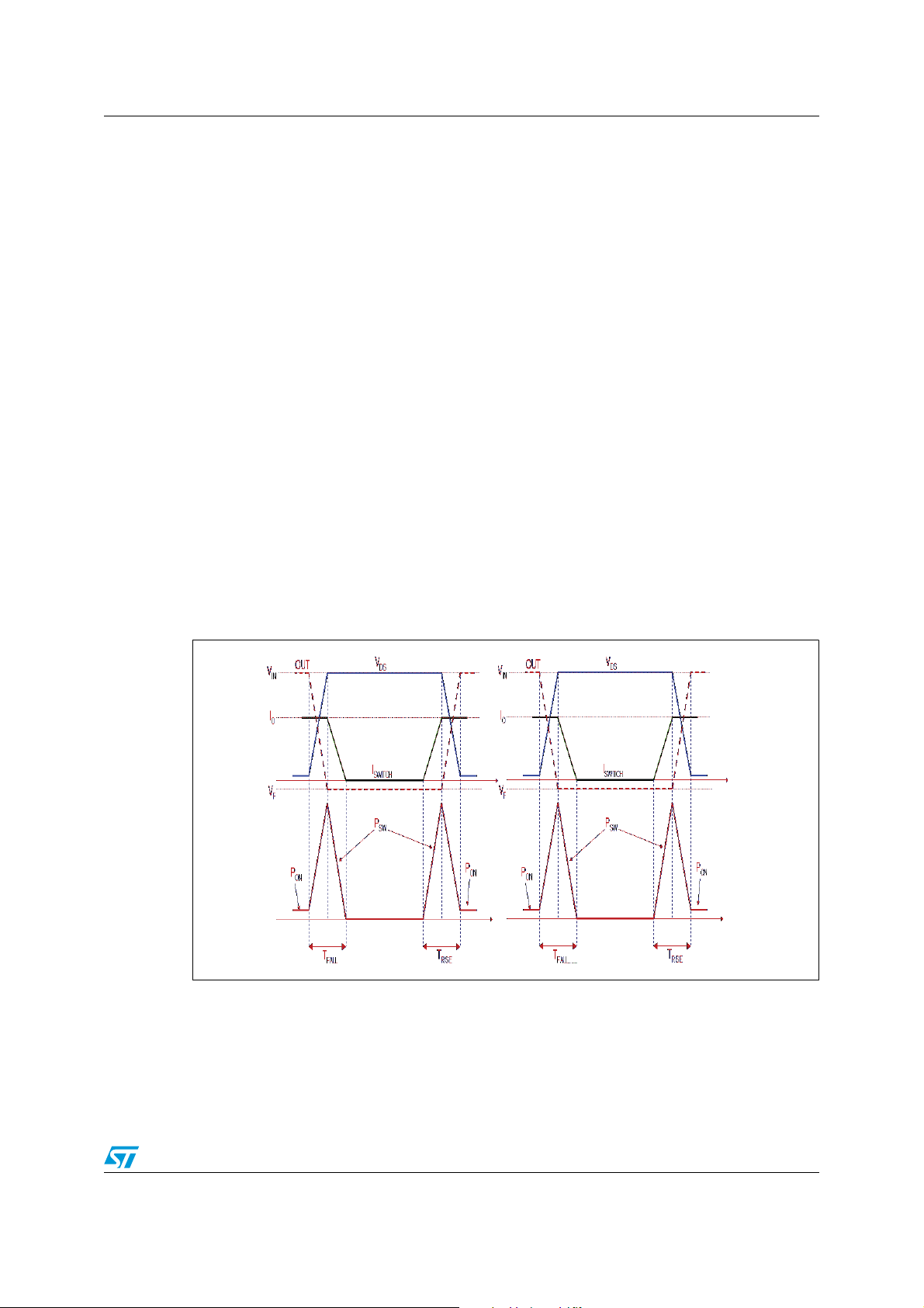
P
ONRRDSON_HSIOUT
()⋅
2
D ⋅=
P
OFFRRDSON_LSIOUT
()⋅
2
1D–()⋅=
P
SWVINIOUT
T
RISETFALL
+()
2
-------------------------------------------
F
SWVIN
= I
OUTTSW_EQFSW
⋅⋅ ⋅ ⋅⋅ ⋅=
PQVINIQ⋅=
7.3 Thermal considerations
The dissipated power of the device is tied to three different sources:
● Conduction losses due to the R
Equation 33
where D is the duty cycle of the application. Note that the duty cycle is theoretically given by
the ratio between V
OUT
(n
LED∗VLED
higher than this value to compensate for the losses in the overall application. For this
reason, the conduction losses related to the R
● Switching losses due to turn-ON and turn-OFF. These are derived using the following
equation:
Equation 34
, which are equal to:
DSON
+ 100 mV) and VIN, but in practice it is substantially
increase compared to an ideal case.
DSON
where T
RISE
and T
represent the switching times of the power element that cause the
FALL
switching losses when driving an inductive load (see Figure 17). T
switching time.
Figure 17. Switching losses
● Quiescent current losses.
is the equivalent
SW
AM12908v1
Equation 35
Example (see Section Example 1):
Doc ID 023432 Rev 2 27/39
Page 28

Application information LED2000
V
OUTnLEDVFW_LEDVFB
+⋅ 7.1V==
P
TOTRDSON_HSIOUT
()⋅
2
DR
DSON_LSIOUT
()⋅
2
1D–()⋅ VINI
OUTfSWTSW
⋅⋅⋅ VINIQ⋅+++⋅=
P
TOT
0.14 0.720.6 0.1 0.720.4⋅⋅ 12+ 0.712109–850 10312 1.5 10
3–
⋅⋅+⋅⋅⋅ ⋅ ⋅+⋅⋅ 205m W≅=
TJTARth
JA–
P
TOT
⋅+=
TJ60 0.205 40 68° C≅⋅+=
VIN=12 V, V
FW_LED
=3.5 V, n
LED
=2, I
=700 mA
LED
The typical output voltage is:
Equation 36
R
DSON_HS
For the calculation we can estimate R
has a typical value of 95 mΩ and R
DSON_HS
DSON_LS
= 140 mΩ and R
consequence of Tj increase during the operation.
T
I
Q
is approximately 12 ns.
SW_EQ
has a typical value of 1.5 mA @ VIN = 12 V.
The overall losses are:
Equation 37
Equation 38
is 69 mΩ @ 25 °C.
DSON_LS
= 100 mΩ as a
The junction temperature of the device is:
Equation 39
where T
is the ambient temperature and Rth
A
ambient. The junction-to-ambient (Rth
HSO8 package and mounted on the board is about 40 °C/W.
Assuming the ambient temperature is around 40 °C, the estimated junction temperature is:
7.4 Short-circuit protection
In overcurrent protection mode, when the peak current reaches the current limit threshold,
the device disables the power element and it is able to reduce the conduction time down to
the minimum value (approximately 100 nsec typical) to keep the inductor current limited.
This is the pulse-by-pulse current limitation to implement the constant current protection
feature.
In overcurrent condition, the duty cycle is strongly reduced and, in most applications, this is
enough to limit the switch current to the current threshold.
is the thermal resistance junction-to-
J-A
) thermal resistance of the device assembled in the
J-A
28/39 Doc ID 023432 Rev 2
Page 29

LED2000 Application information
I
L TON
Δ
V
INVOUT
– DCRLR
DSON HS
+()I⋅–
L
--------------------------------------------------------------- ----------------------------------------
T
ON
()=
I
L TON
Δ
V
OUT
DCRLR
DSON LS
+()I⋅+()–
L
------------------------------------------------------------- ----------------------------------
T
OFF
()=
I
L TON
Δ I
L TOFF
Δ=
I
L TON
Δ
V
IN
DCRLR
DSON HS
+()I⋅–
L
------------------------------------------------------- ------------------------
T
ON MIN
()
V
IN
L
---------
90ns()≅=
I
L TOFF
Δ
DCR
LRDSON LS
+()– I⋅
L
-------------------------------------------------------- ------------
T
SW
90ns–()
DCR
LRDSON LS
+()– I⋅
L
----------------------------------------------------------- ---------
1.18μs()≅=
The inductor current ripple during ON and OFF phases can be written as:
● ON phase
Equation 40
● OFF phase
Equation 41
where DCR
is the series resistance of the inductor.
L
The pulse-by-pulse current limitation is effective to implement constant current protection
when:
Equation 42
From Equation 40 and Equation 41 it can be seen that the implementation of the constant
current protection becomes more critical the lower the V
and the higher the VIN.
OUT
In fact, in short-circuit condition the voltage applied to the inductor during the OFF-time
becomes equal to the voltage drop across parasitic components (typically the DCR of the
inductor and the R
the voltage applied at the inductor is maximized and is approximately equal to V
of the low-side switch) since VOUT is negligible, while during TON
DSON
IN
.
In general, the worst case scenario is heavy short-circuit at the output with maximum input
voltage. Equation 40 and Equation 41 in overcurrent conditions can be simplified to:
Equation 43
considering T
which has already been reduced to its minimum.
ON
Equation 44
where T
=1/fSW and considering the nominal fSW.
SW
At higher input voltage
escalate. As a consequence, the system typically meets Equation 42 at a current level
higher than the nominal value thanks to the increased voltage drop across stray
components. In most of the application conditions the pulse-by-pulse current limitation is
effective to limit the inductor current. Whenever the current escalates, a second level current
protection called “Hiccup mode” is enabled. Hiccup protection offers an additional protection
against heavy short-circuit conditions at very high input voltage even considering the spread
ΔI
L TON
may be higher than ΔI
and so the inductor current can
L TOFF
Doc ID 023432 Rev 2 29/39
Page 30

Application information LED2000
AM12909v1
SIGNAL'.$
POWER'.$
N&6
#
6,%$
U6
#
2 +
6).
'.$
2
.-
23
$)-
6).?!
$)-
&"
!'.$
0'.$
37
6).?37
%0
34##
U6
#
,
U(
,
*0
6,%$
!-V
of the minimum conduction time of the power element. If the hiccup current level (6.2 A
typical) is triggered, the switching activity is prevented for 12 cycles.
Figure 18 shows the operation of the constant current protection when a short-circuit is
applied at the output at the maximum input voltage.
Figure 18. Constant current protection triggering Hiccup mode
7.5 Application circuit
Figure 19. Demonstration board application circuit
30/39 Doc ID 023432 Rev 2
Page 31
LED2000 Application information
Table 8. Component list
Reference Part number Description Manufacturer
C1
C2 GRM31CR61E106KA12L
C3 GRM21BR71E225KA73L
R1
R2 Not mounted
Rs ERJ14BSFR15U
L1 XAL6060-223ME
Figure 20. PCB layout (component side)
100 nF 50 V
(size 0805)
10 μF 25 V
(size 1206)
2.2 μF 25 V
(size 0805)
4.7 KΩ 5%
(size 0603)
0.15 Ω 1%
(size 1206)
22 μH
I
=5.6 A (30%
SAT
drop)I
=6.9 A (40 °C
RMS
rise)
(size 6.36 x 6.56 x 6.1 mm)
Murata
Murata
Panasonic
Coilcraft
Doc ID 023432 Rev 2 31/39
Page 32

Application information LED2000
Figure 21. PCB layout (bottom side)
32/39 Doc ID 023432 Rev 2
Page 33

LED2000 Typical characteristics
AM12915v1
AM12916v1
To maximize the dimming
performance the embedded LS
discharg es C
OUT
when DIM goes lo w.
(DIM = 0 & & VFB> 60mV ):
the lo w sid e is enable d
as lon g as I
L
> -1A
(implements negative
cu rrent limitation )
AM12917v1
8 Typical characteristics
Figure 22. Soft-start Figure 23. Load regulation
Vin 12V
Vled 7V
AM12913v1
Figure 24. Dimming operation Figure 25. LED current rising edge
a
Figure 26. LED current falling edge Figure 27. Hiccup current protection
AM12914v1
AM12918v1
Doc ID 023432 Rev 2 33/39
Page 34

Ordering information LED2000
AM12920v1
Figure 28. Efficiency vs. IOUT (VIN 32 V) Figure 29. Thermal shutdown protection
130 ns typ.
AM12919v1
9 Ordering information
Table 9. Ordering information
Order code Package Packaging
LED2000PUR VFQFPN 4x4 8L Tape and reel
LED2000DR SO-8BW Tape and reel
34/39 Doc ID 023432 Rev 2
Page 35

LED2000 Package mechanical data
10 Package mechanical data
In order to meet environmental requirements, ST offers these devices in different grades of
®
ECOPACK
specifications, grade definitions and product status are available at: www.st.com.
ECOPACK
packages, depending on their level of environmental compliance. ECOPACK®
®
is an ST trademark.
Table 10. VFQFPN8 (4x4x1.08 mm) mechanical data
mm
Dim.
Min. Typ. Max.
A 0.80 0.90 1.00
A1 0.02 0.05
A3 0.20
b 0.23 0.30 0.38
D 3.90 4.00 4.10
D2 2.82 3.00 3.23
E 3.90 4.00 4.10
E2 2.05 2.20 2.30
e0.80
L 0.40 0.50 0.60
Doc ID 023432 Rev 2 35/39
Page 36

Package mechanical data LED2000
Figure 30. VFQFPN8 (4x4x1.08 mm) package dimensions
Table 1 1. SO-8 mechanical data
mm
Dim.
Min. Typ. Max.
A 1.75
A1 0.10 0.25
A2 1.25
b0.28 0.48
c0.17 0.23
D4.804.905.00
E5.806.006.20
E1 3.80 3.90 4.00
e1.27
h0.25 0.50
L0.40 1.27
L1 1.04
k0° 8°
ccc 0.10
36/39 Doc ID 023432 Rev 2
Page 37

LED2000 Package mechanical data
0016023_Rev_E
Figure 31. SO8 package dimensions
Doc ID 023432 Rev 2 37/39
Page 38

Revision history LED2000
11 Revision history
Table 12. Document revision history
Date Revision Changes
11-Jul-2012 1 Initial release.
27-Jul-2012 2 Document status promoted form preliminary to production data.
38/39 Doc ID 023432 Rev 2
Page 39

LED2000
Please Read Carefully:
Information in this document is provided solely in connection with ST products. STMicroelectronics NV and its subsidiaries (“ST”) reserve the
right to make changes, corrections, modifications or improvements, to this document, and the products and services described herein at any
time, without notice.
All ST products are sold pursuant to ST’s terms and conditions of sale.
Purchasers are solely responsible for the choice, selection and use of the ST products and services described herein, and ST assumes no
liability whatsoever relating to the choice, selection or use of the ST products and services described herein.
No license, express or implied, by estoppel or otherwise, to any intellectual property rights is granted under this document. If any part of this
document refers to any third party products or services it shall not be deemed a license grant by ST for the use of such third party products
or services, or any intellectual property contained therein or considered as a warranty covering the use in any manner whatsoever of such
third party products or services or any intellectual property contained therein.
UNLESS OTHERWISE SET FORTH IN ST’S TERMS AND CONDITIONS OF SALE ST DISCLAIMS ANY EXPRESS OR IMPLIED
WARRANTY WITH RESPECT TO THE USE AND/OR SALE OF ST PRODUCTS INCLUDING WITHOUT LIMITATION IMPLIED
WARRANTIES OF MERCHANTABILITY, FITNESS FOR A PARTICULAR PURPOSE (AND THEIR EQUIVALENTS UNDER THE LAWS
OF ANY JURISDICTION), OR INFRINGEMENT OF ANY PATENT, COPYRIGHT OR OTHER INTELLECTUAL PROPERTY RIGHT.
UNLESS EXPRESSLY APPROVED IN WRITING BY TWO AUTHORIZED ST REPRESENTATIVES, ST PRODUCTS ARE NOT
RECOMMENDED, AUTHORIZED OR WARRANTED FOR USE IN MILITARY, AIR CRAFT, SPACE, LIFE SAVING, OR LIFE SUSTAINING
APPLICATIONS, NOR IN PRODUCTS OR SYS
TEMS WHERE FAILURE OR MALFUNCTION MAY RESULT IN PERSONAL INJURY,
DEATH, OR SEVERE PROPERTY OR ENVIRONMENTAL DAMAGE. ST PRODUCTS WHICH ARE NOT SPECIFIED AS "AUTOMOTIVE
GRADE" MAY ONLY BE USED IN AUTOMOTIVE APPLICATIONS AT USER’S OWN RISK.
Resale of ST products with provisions different from the statements and/or technical features set forth in this document shall immediately void
any warranty granted by ST for the ST product or service described herein and shall not create or extend in any manner whatsoever, any
liability of ST.
ST and the ST logo are trademarks or registered trademarks of ST in various countries.
Information in this document supersedes and replaces all information previously supplied.
The ST logo is a registered trademark of STMicroelectronics. All other names are the property of their respective owners.
© 2012 STMicroelectronics - All rights reserved
STMicroelectronics group of companies
Australia - Belgium - Brazil - Canada - China - Czech Republic - Finland - France - Germany - Hong Kong - India - Israel - Italy - Japan -
Malaysia - Malta - Morocco - Philippines - Singapore - Spain - Sweden - Switzerland - United Kingdom - United States of America
www.st.com
Doc ID 023432 Rev 2 39/39
 Loading...