

Very low dropout voltage regulators with inhibit function
Features
■ Very low dropout voltage (0.2 V typ.)
■ Very low quiescent current (typ. 50 µA in OFF
mode, 0.5 mA in ON mode, no load)
■ Output current up to 100 mA
■ Output voltages of 3 V, 3.3 V, 4.5 V, 5 V, 8 V
■ Internal current and thermal limit
■ Small 2.2 µF capacitor for stability
■ Available in ± 1% (A) or ± 2% (C) selection at
25 °C
■ Supply voltage rejection: 80 dB (typ.)
■ Temperature range: - 40 to 125 °C
Description
The LExxAB and LExxC are very low dropout
voltage regulators available in SO-8 and TO-92
packages and over a wide range of output
voltages.
The very low dropout voltage (0.2 V) and the very
low quiescent current make them particularly
suitable for low-noise low-power applications and
especially in battery-powered systems.
LExxAB
LExxC
Datasheet − production data
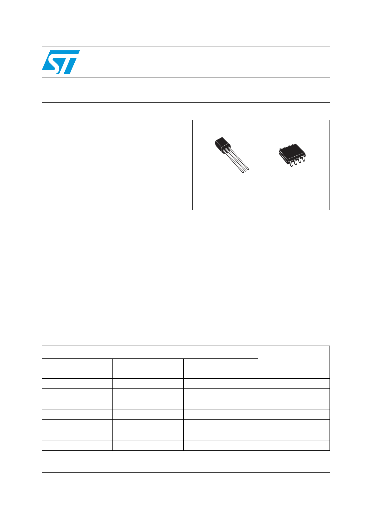
TO-92
These devices are pin-to-pin compatible with the
older L78Lxx series. Furthermore, in the 8-pin
configuration (SO-8) they employ a shutdown
logic control (pin 5, TTL compatible). This means
that when the device is used as a local regulator,
a part of the board can be put in standby,
decreasing even more total power consumption.
In the three-terminal configuration (TO-92) the
device is always in the ON state, maintaining the
same electrical performance. It requires only a
2.2 µF capacitor for stability, reducing component
size and cost.
SO-8
Table 1. Device summary
Order codes
SO-8
(tape and reel)
LE30CD-TR 3 V
LE33CD-TR LE33CZ-TR LE33CZ-AP 3.3 V
LE45CD-TR 4.5 V
LE50ABD-TR LE50ABZ-AP 5 V
LE50CD-TR 5 V
LE80CD-TR 8 V
May 2012 Doc ID 2573 Rev 13 1/22
This is information on a product in full production.
TO-92
(tape and reel)
LE30ABZ-TR 3 V
TO-92 (Ammopak)
Output voltages
www.st.com
22

Contents LExxAB, LExxC
Contents
1 Diagram . . . . . . . . . . . . . . . . . . . . . . . . . . . . . . . . . . . . . . . . . . . . . . . . . . . 3
2 Pin configuration . . . . . . . . . . . . . . . . . . . . . . . . . . . . . . . . . . . . . . . . . . . 4
3 Maximum ratings . . . . . . . . . . . . . . . . . . . . . . . . . . . . . . . . . . . . . . . . . . . . 5
4 Electrical characteristics . . . . . . . . . . . . . . . . . . . . . . . . . . . . . . . . . . . . . 6
5 Typical performance characteristics . . . . . . . . . . . . . . . . . . . . . . . . . . . 13
6 Package mechanical data . . . . . . . . . . . . . . . . . . . . . . . . . . . . . . . . . . . . 16
7 Revision history . . . . . . . . . . . . . . . . . . . . . . . . . . . . . . . . . . . . . . . . . . . 21
2/22 Doc ID 2573 Rev 13
LExxAB, LExxC Diagram
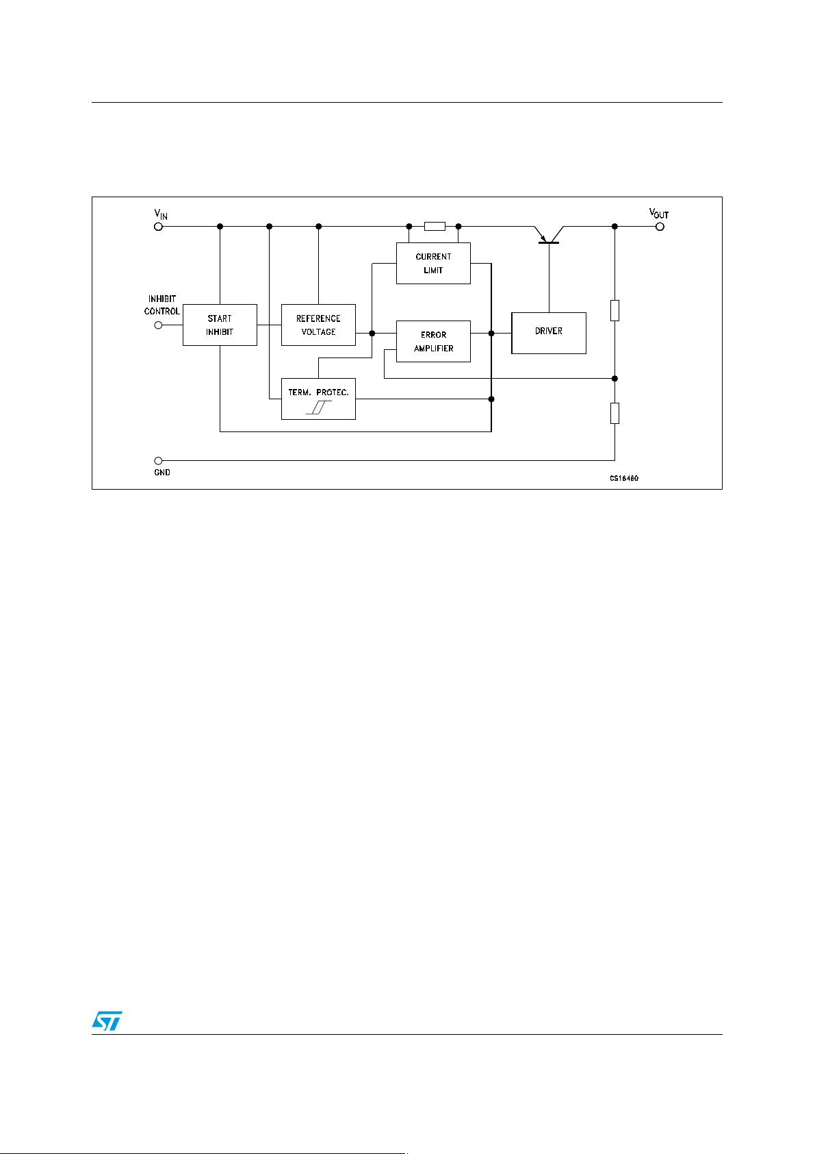
1 Diagram
Figure 1. Block diagram
Doc ID 2573 Rev 13 3/22
Pin configuration LExxAB, LExxC
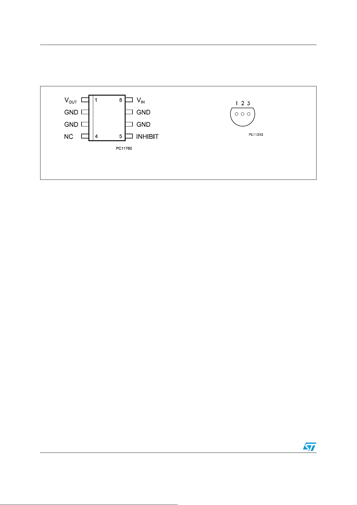
2 Pin configuration
Figure 2. Pin connections (top view for SO-8, bottom view for TO-92)
SO-8
PIN 1 = V
OUT
PIN 2 = GND
PIN 3 = V
IN
TO-92
4/22 Doc ID 2573 Rev 13
LExxAB, LExxC Maximum ratings
3 Maximum ratings
Table 2. Absolute maximum ratings
Symbol Parameter Value Unit
V
I
I
O
P
TOT
T
STG
T
OP
1. Our SO-8 package used for voltage regulators is modified internally to have pins 2, 3, 6 and 7 electrically fused to the die
attach pad. This particular frame decreases the total thermal resistance of the package and increases its ability to dissipate
power when an appropriate area of copper on the printed circuit board is available for heatsinking. The external dimensions
are the same as for the standard SO-8.
DC input voltage 20 V
Output current Internally limited
(1)
Power dissipation Internally limited
Storage temperature range -65 to 150 °C
Operating junction temperature range -40 to 125 °C
Table 3. Thermal data
Symbol Parameter SO-8 TO-92 Unit
R
thJC
R
thJA
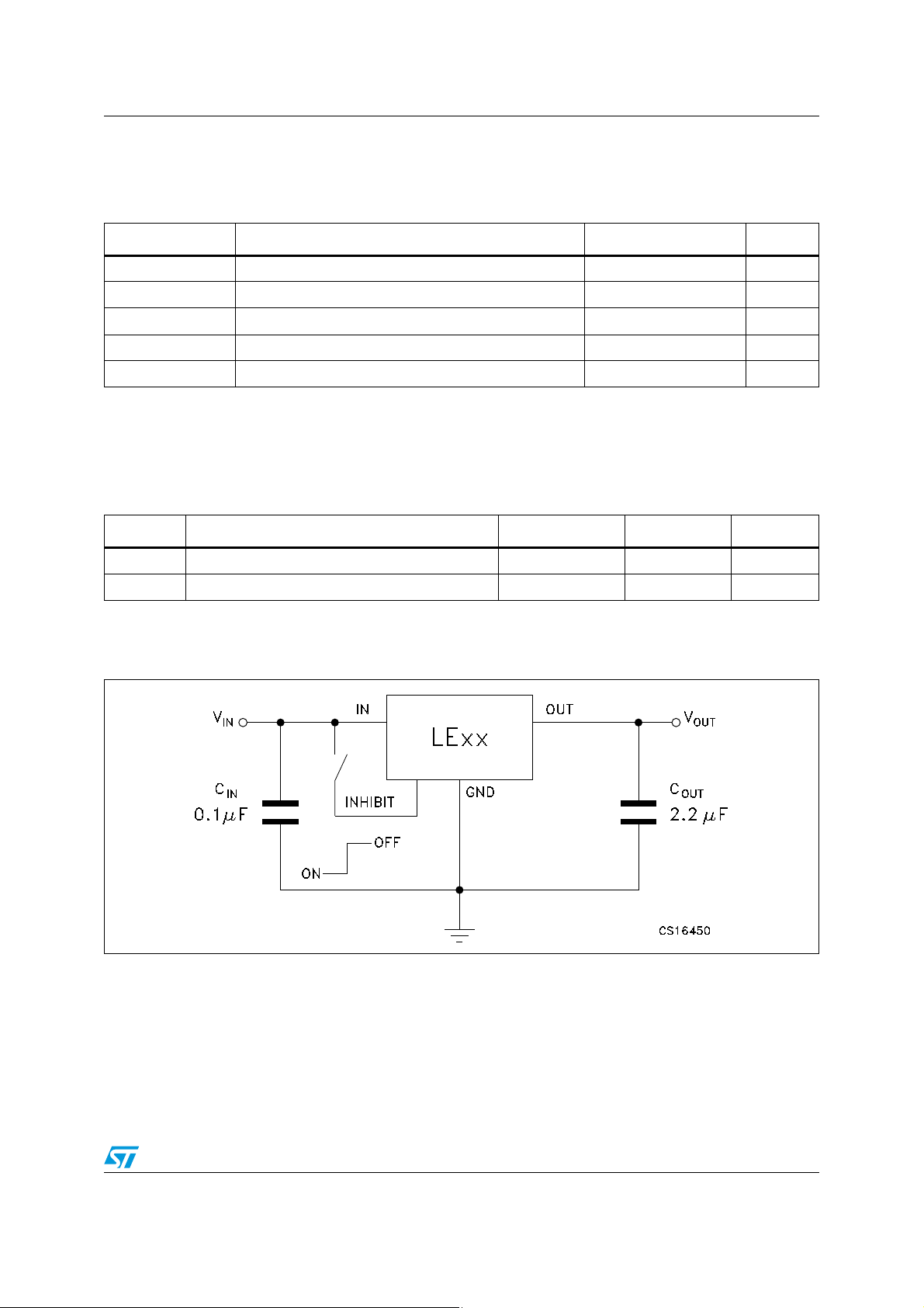
Figure 3. Test circuit
Thermal resistance junction-case 20 °C/W
Thermal resistance junction-ambient 55 200 °C/W
Note: If the INHIBIT pin is left floating, the regulator is in the ON mode. However, to avoid picking
up any noise, it is suggested to ground it when the Inhibit function is not used.
Doc ID 2573 Rev 13 5/22
Electrical characteristics LExxAB, LExxC
4 Electrical characteristics
Refer to the test circuits, TJ = 25 °C, CI = 0.1 µF, CO = 2.2 µF unless otherwise specified.
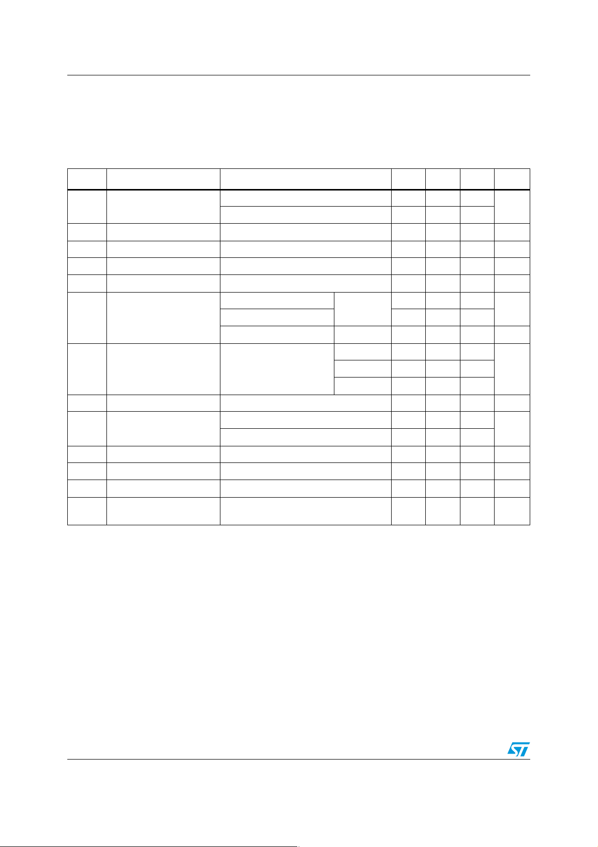
Table 4. Electrical characteristics for LE30AB
Symbol Parameter Test conditions Min. Typ. Max. Unit
V
O
V
I
I
O
ΔV
O
ΔV
O
I
d
I
= 10 mA, VI = 5 V 2.970 3 3.030
Output voltage
O
= 10 mA, VI = 5 V, TJ = -25 to 85°C 2.940 3.060
I
O
V
Operating input voltage IO = 100 mA 18 V
Output current limit 150 mA
Line regulation VI = 3.7 to 18 V, IO = 0.5 mA 3 15 mV
Load regulation VI = 4 V, IO = 0.5 to 100 mA 3 15 mV
Quiescent current
= 4 to 18 V, IO = 0 mA
V
I
= 4 to 18 V, IO = 100 mA 1.5 3
V
I
V
= 6 V OFF mode 50 100 µA
I
ON mode
0.5 1
mA
f = 120 Hz 81
SVR Supply voltage rejection I
= 5 mA, VI = 5 ± 1 V
O
f = 10 kHz 60
eN Output noise voltage B = 10 Hz to 100 kHz 50 µV
I
= 100 mA 0.2 0.4
V
Dropout voltage
d
V
Control input logic low TJ = -40 to 125°C 0.8 V
IL
V
Control input logic high TJ = -40 to 125°C 2 V
IH
I
Control input current VI = 6 V, VC = 6 V 10 µA
I
Output bypass
C
O
capacitance
O
= 100 mA, TJ = -40 to 125°C 0.5
I
O
ESR = 0.1 to 10 Ω, I
= 0 to 100 mA 2 10 µF
O
dBf = 1 kHz 76
V
6/22 Doc ID 2573 Rev 13
LExxAB, LExxC Electrical characteristics
Refer to the test circuits, TJ = 25 °C, CI = 0.1 µF, CO = 2.2 µF unless otherwise specified.
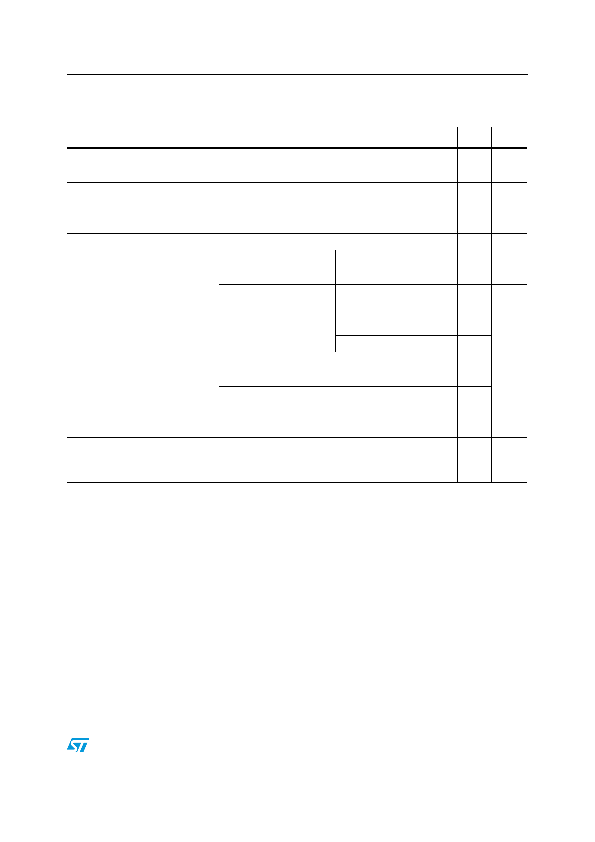
Table 5. Electrical characteristics for LE30C
Symbol Parameter Test conditions Min. Typ. Max. Unit
V
O
V
I
I
O
ΔV
O
ΔVOLoad regulation VI = 4 V, IO = 0.5 to 100 mA 3 25 mV
I
= 10 mA, VI = 5 V 2.940 3 3.060
Output voltage
O
= 10 mA, VI = 5 V, TJ = -25 to 85°C 2.880 3.120
I
O
V
Operating input voltage IO = 100 mA 18 V
Output current limit 150 mA
Line regulation VI = 3.7 to 18 V, IO = 0.5 mA 3 20 mV
Quiescent current
I
d
= 4 to 18 V, IO = 0 mA
V
I
= 4 to 18 V, IO = 100 mA 1.5 3
V
I
ON mode
0.5 1
VI = 6 V OFF mode 50 100 µA
f = 120 Hz 81
SVR Supply voltage rejection I
= 5 mA, VI = 5 ± 1 V
O
f = 10 kHz 60
eN Output noise voltage B = 10 Hz to 100 kHz 50 µV
I
= 100 mA 0.2 0.4
V
Dropout voltage
d
V
Control input logic low TJ = -40 to 125°C 0.8 V
IL
V
Control input logic high TJ = -40 to 125°C 2 V
IH
I
Control input current VI = 6 V, VC = 6 V 10 µA
I
Output bypass
C
O
capacitance
O
IO = 100 mA, TJ = -40 to 125°C 0.5
ESR = 0.1 to 10 Ω, I
= 0 to 100 mA 2 10 µF
O
mA
dBf = 1kHz 76
V
Doc ID 2573 Rev 13 7/22
 Loading...