

Features
■ Input voltage from 1.5 to 5.5 V
■ Ultra low dropout voltage (200 mV typ. at 500
mA load)
■ Very low quiescent current (20 µA typ. at no
load, 100 µA typ. at 500 mA load, 1 µA max in
off mode)
■ Very low noise without bypass capacitor
■ Output voltage tolerance: ± 2.0 % @ 25 °C
■ 500 mA guaranteed output current
■ Wide range of output voltages available on
request: 0.8 V to 4.5 V with 100 mV step and
ADJ from 0.8 V
■ Logic-controlled electronic shutdown
■ Compatible with ceramic capacitor
C
= 1 µF
OUT
■ Internal current and thermal limit
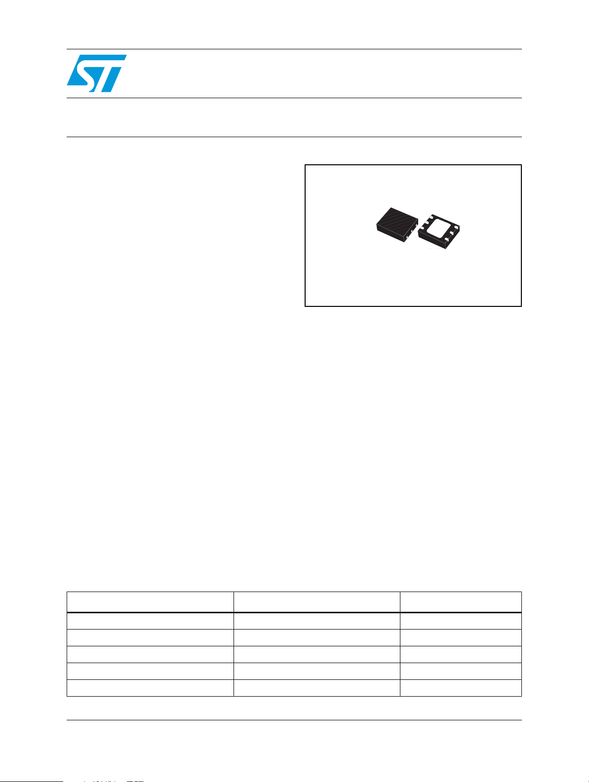
■ Package DFN6 (3 x 3 mm)
■ Temperature range: -40 °C to 125 °C
LD39050xx
500 mA low quiescent current
low noise voltage regulator
DFN6 (3 x 3 mm)
roll off at 10 kHz. An Enable logic control function
puts the LD39050 in shut-down mode allowing a
total current consumption lower than 1 µA. The
device also includes short-circuit constant current
limiting and thermal protection. Typical
applications are mobile phones, personal digital
assistants (PDAs), cordless phones and similar
battery-powered systems.
Description
The LD39050 provides 500 mA maximum current
from an input voltage ranging from 1.5 V to 5.5 V
with a typical dropout voltage of 200 mV. Stability
is provided using ceramic capacitors. The ultra
low drop-voltage, low quiescent current and low
noise features make it suitable for low power
battery-powered applications. Power supply
rejection is 65 dB at low frequencies and starts to
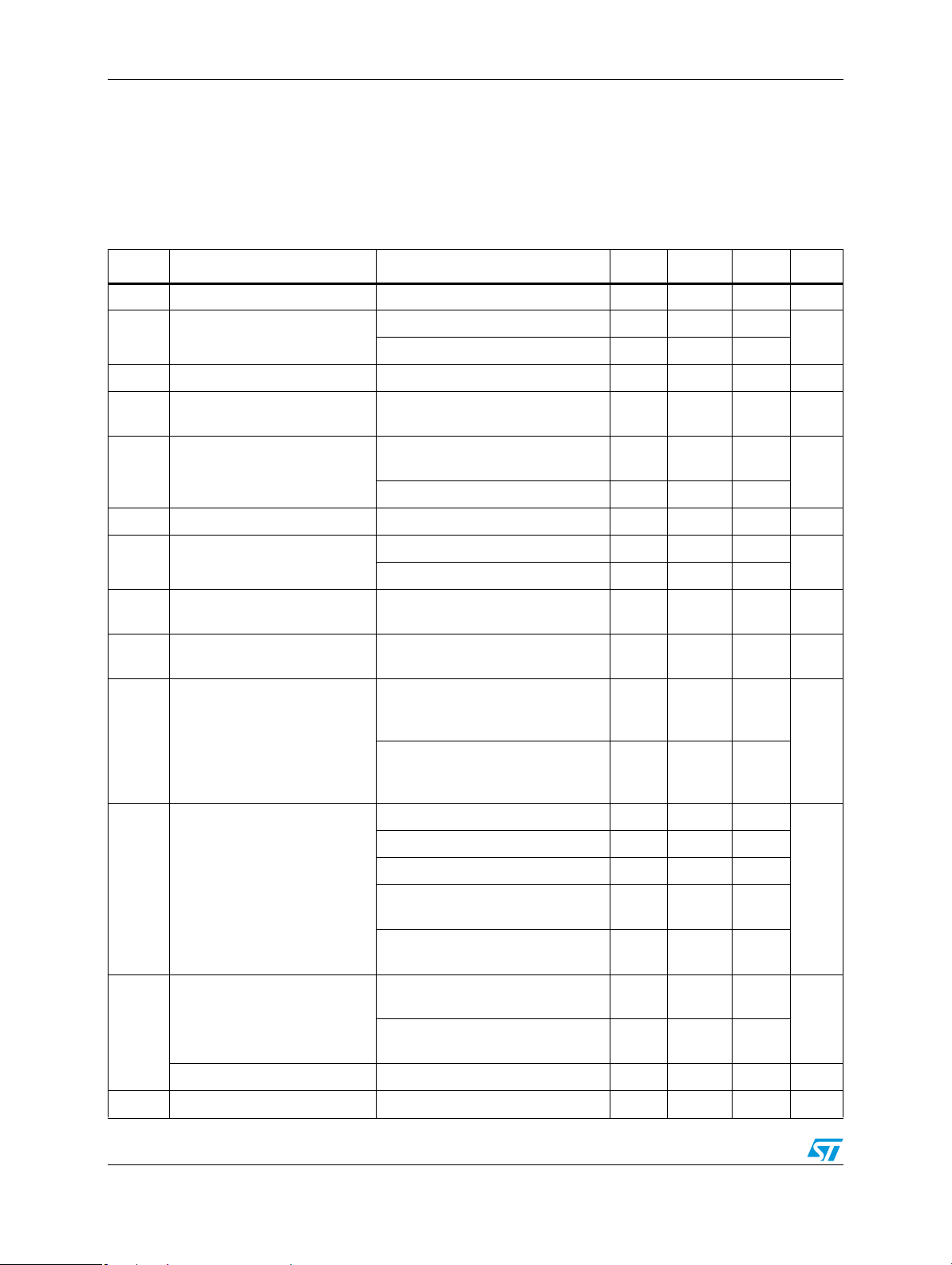
Table 1. Device summary
Part numbers Order codes Output voltages
LD39050XX LD39050PUR ADJ from 0.8 V
LD39050XX10 LD39050PU10R 1.0 V
LD39050XX12 LD39050PU12R 1.2 V
LD39050XX25 LD39050PU25R 2.5 V
LD39050XX33 LD39050PU33R 3.3 V
March 2009 Rev 1 1/24
www.st.com
24

Contents LD39050xx
Contents
1 Diagrams . . . . . . . . . . . . . . . . . . . . . . . . . . . . . . . . . . . . . . . . . . . . . . . . . . 3
2 Pin configuration . . . . . . . . . . . . . . . . . . . . . . . . . . . . . . . . . . . . . . . . . . . 4
3 Maximum ratings . . . . . . . . . . . . . . . . . . . . . . . . . . . . . . . . . . . . . . . . . . . . 5
4 Electrical characteristics . . . . . . . . . . . . . . . . . . . . . . . . . . . . . . . . . . . . . 6
5 Typical performance characteristics . . . . . . . . . . . . . . . . . . . . . . . . . . . 10
6 Application information . . . . . . . . . . . . . . . . . . . . . . . . . . . . . . . . . . . . . 15
6.1 Power dissipation . . . . . . . . . . . . . . . . . . . . . . . . . . . . . . . . . . . . . . . . . . . 16
6.2 Enable function . . . . . . . . . . . . . . . . . . . . . . . . . . . . . . . . . . . . . . . . . . . . . 16
6.3 Power Good function . . . . . . . . . . . . . . . . . . . . . . . . . . . . . . . . . . . . . . . . 16
7 Package mechanical data . . . . . . . . . . . . . . . . . . . . . . . . . . . . . . . . . . . . 18
8 Different output voltage versions of the LD39050xx
available on request . . . . . . . . . . . . . . . . . . . . . . . . . . . . . . . . . . . . . . . . 22
9 Revision history . . . . . . . . . . . . . . . . . . . . . . . . . . . . . . . . . . . . . . . . . . . 23
2/24
LD39050xx Diagrams
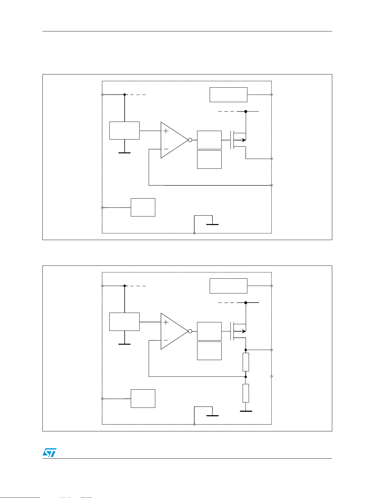
1 Diagrams
Figure 1. Schematic diagram for the LD39050PU
IN
IN
BandGap
BandGap
reference
reference
OpAmp
OpAmp
EN
EN
Figure 2. Schematic diagram for the LD39050PUxx
Internal
Internal
enable
enable
GND
GND
Power-good
Power-good
Current
Current
limit
limit
Thermal
Thermal
protection
protection
signal
signal
PG
PG
IN
ININ
OUT
OUT
ADJ
ADJ
IN
IN
EN
EN
BandGap
BandGap
reference
reference
Internal
Internal
enable
enable
OpAmp
OpAmp
GND
GND
Power-good
Power-good
Current
Current
limit
limit
Thermal
Thermal
protection
protection
signal
signal
PG
PG
IN
ININ
OUT
OUT
R
R
1
1
NC
NC
R
R
2
2
3/24
Pin configuration LD39050xx
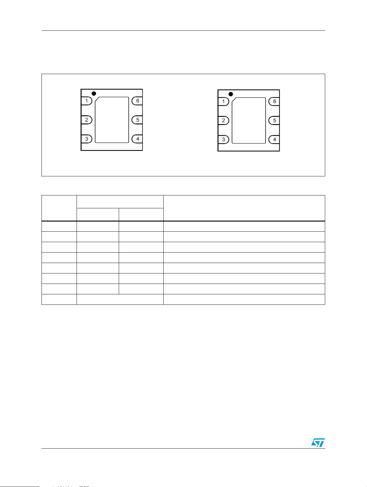
2 Pin configuration
Figure 3. Pin connection (top view)
EN
GND
PG
LD39050PUxx
V
NC
V
IN
OUT
EN
GND
PG
LD39050PU
Table 2. Pin description
Pin n°
Symbol
LD39050PU LD39050PUxx
EN 1 1 Enable pin logic input: Low=shutdown, High=active
GND 2 2 Common ground
PG 3 3 Power Good
V
OUT
4 4 Output voltage
ADJ 5 - Adjust pin
V
IN
6 6 Input voltage of the LDO
NC - 5 Not connected
GND EXP pad Exposed pad must be connected to GND
Function
V
IN
ADJ
V
OUT
4/24
LD39050xx Maximum ratings
3 Maximum ratings
Table 3. Absolute maximum ratings
Symbol Parameter Value Unit
V
IN
V
OUT
EN Enable pin -0.3 to V
DC input voltage -0.3 to 7 V
DC output voltage -0.3 to VI + 0.3 (7 V max) V
+ 0.3 (7 V max) V
I
PG Power Good pin -0.3 to 7 V
ADJ Adjust pin 4 V
I
T
T
OUT
P
D
STG
OP
Output current Internally limited
Power dissipation Internally limited
Storage temperature range - 65 to 150 °C
Operating junction temperature range - 40 to 125 °C
Note: Absolute maximum ratings are those values beyond which damage to the device may occur.
Functional operation under these conditions is not implied. All values are referred to GND.
Table 4. Thermal data
Symbol Parameter Value Unit
R
R
thJA
thJC
Thermal resistance junction-ambient 55 °C/W
Thermal resistance junction-case 10 °C/W
Table 5. ESD performance
Symbol Parameter Test conditions Value Unit
HBM 2 kV
ESD ESD protection voltage
MM 0.3 kV
5/24
Electrical characteristics LD39050xx
4 Electrical characteristics
TJ = 25 °C, V
= 1.8 V, CIN = C
IN
OUT
= 1 µF, I
= 10 mA, VEN = VIN, unless otherwise
OUT
specified.
Table 6. Electrical characteristics for the LD39050PU
Symbol Parameter Test conditions Min. Typ. Max. Unit
V
IN
V
ADJVADJ
I
ADJ
ΔV
OUT
ΔV
OUT
ΔV
OUT
ΔV
OUT
V
DROP
Operating input voltage 1.5 5.5 V
I
=10 mA, TJ = 25°C 784 800 816
accuracy
OUT
= 10 mA, -40°C<TJ<125°C 776 800 824
I
OUT
mV
Adjust pin current 1µA
+1 V ≤ VIN ≤ 5.5 V,
V
Static line regulation
Transient line regulation
(1)
Static load regulation I
Transient load regulation
Dropout voltage
(2)
(1)
OUT
= 1 mA
I
OUT
ΔVIN=500 mV, I
=10 mA, tR=5
OUT
µs
ΔV
=500 mV, I
IN
= 10 mA to 500 mA 0.002 %/mA
OUT
I
= 10 mA to 500 mA, tR=5µs 40
OUT
= 10 mA to 500 mA, tF=5µs 40
I
OUT
IO = 500mA, V
=10 mA, tF=5 µs 10
OUT
fixed to 1.5V
OUT
40°C<TJ<125°C
0.01 %/V
10
200 400 mV
mVpp
mVpp
e
N
SVR
I
Q
PG
I
SC
Output noise voltage
Supply voltage rejection
= 0.8V
V
OUT
Quiescent current
Power Good output threshold
10Hz to 100kHz, I
V
= 0.8 V
OUT
VIN = 1.8V+/-V
V
I
V
V
I
I
I
I
I
40°C<T
V
V
= 0.25V, freq. = 1kHz
RIPPLE
= 10 mA
OUT
= 1.8V+/-V
IN
= 0.25V, freq.=10 kHz
RIPPLE
= 100 mA
OUT
= 0 mA 20
OUT
= 0 mA, -40°C<TJ<125°C 50
OUT
= 0 to 500mA 100
OUT
=0 to 500mA, -
OUT
<125°C
J
input current in off mode:
IN
EN
= GND
(3)
Rising edge
Falling edge
OUT
RIPPLE
RIPPLE
= 100 mA,
30 µV
65
62
200
0.001 1
0.92*
V
OUT
0.8*
V
OUT
RMS
dB
µA
V
Power Good output voltage low Isink=6mA open drain output 0.4 V
Short-circuit current RL=0 600 800 mA
6/24
LD39050xx Electrical characteristics
Table 6. Electrical characteristics for the LD39050PU (continued)
Symbol Parameter Test conditions Min. Typ. Max. Unit
V
EN
Enable input logic high V
I
Enable pin input current VEN= V
EN
t
ON
Turn on time
(4)
=1.5 V to 5.5 V, 40°C<TJ<125°C 0.9 V
IN
IN
0.1 100 nA
30 µs
Thermal shutdown 160
Enable input logic low VIN=1.5 V to 5.5 V, 40°C<TJ<125°C 0.4 V
T
SHDN
Hysteresis 20
°C
Capacitance (see typical
C
Output capacitor
OUT
performance characteristics for
122µF
stability)
1. All transient values are guaranteed by design, not production tested
2. Dropout voltage is the input-to-output voltage difference at which the output voltage is 100 mV below its nominal value. This
specification does not apply for output voltages below 1.5 V
3. PG pin floating
4. Turn-on time is time measured between the enable input just exceeding V
reaching 95% of its nominal value
high value and the output voltage just
EN
7/24
Electrical characteristics LD39050xx
TJ = 25 °C, V
IN
= V
OUT(NOM)
+ 1 V, CIN = C
OUT
= 1 µF, I
= 10 mA, VEN = VIN, unless
OUT
otherwise specified.
Table 7. Electrical characteristics for the LD39050PUxx
Symbol Parameter Test conditions Min. Typ. Max. Unit
V
IN
V
OUTVOUT
ΔV
OUT
ΔV
OUT
ΔV
OUT
ΔV
OUT
V
DROP
Operating input voltage 1.5 5.5 V
V
accuracy
Static line regulation
Transient line regulation
(1)
Static load regulation I
Transient load regulation
Dropout voltage
(2)
(1)
>1.5V, I
OUT
= 25°C
T
J
>1.5 V, I
V
OUT
-40°C<T
V
OUT
V
OUT
-40°C<T
V
OUT
I
OUT
<125°C
J
≤ 1.5 V, I
≤ 1.5 V, I
<125°C
J
+1 V ≤ VIN ≤ 5.5 V,
= 1 mA
ΔVIN=500 mV, I
=500 mV, I
ΔV
IN
= 10 mA to 500 mA 0.002 %/mA
OUT
I
= 10 mA to 500 mA, tR=5µs 40
OUT
= 10 mA to 500 mA, tF=5µs 40
I
OUT
I
= 500mA, V
OUT
-40°C<TJ<125°C
=10 mA,
OUT
= 10 mA,
OUT
= 10 mA ±20
OUT
=10 mA,
OUT
=10 mA, tR=5 µs 10
OUT
=10 mA, tF=5 µs 10
OUT
> 1.5 V
OUT
-2.0 2.0
-3.0 3.0
±30
mV
0.01 %/V
mVpp
mVpp
200 400 mV
%
e
N
SVR
I
Q
PG
I
SC
Output noise voltage 10Hz to 100kHz, IO = 100 mA, 30 µV
Supply voltage rejection
V
= 1.5V
OUT
Quiescent current
Power Good output threshold
Power Good output voltage
low
VIN = V
OUT(NOM
V
I
V
V
I
I
I
I
I
V
V
= 0.1V, freq. = 1kHz
RIPPLE
= 10 mA
OUT
= V
IN
OUT(NOM)
= 0.1V, freq.=10 kHz
RIPPLE
= 100 mA
OUT
= 0 mA 20
OUT
= 0 mA, -40°C<TJ<125°C 50
OUT
= 0 to 500mA 100
OUT
= 0 to 500mA -40°C<TJ<125°C 200
OUT
input current in off mode:
IN
= GND
EN
Rising edge
Falling edge
Isink=6mA open drain output 0.4 V
)+0.5V+/-V
+0.5V+/-V
(3)
RIPPLE
RIPPLE
65
62
0.001 1
0.92*
V
OUT
0.8*
V
OUT
RMS
dB
µA
V
Short-circuit current RL=0 600 800 mA
8/24

LD39050xx Electrical characteristics
Table 7. Electrical characteristics for the LD39050PUxx (continued)
Symbol Parameter Test conditions Min. Typ. Max. Unit
V
EN
Enable input logic high V
I
Enable pin input current V
EN
t
ON
Turn on time
(4)
=1.5 V to 5.5 V, -40°C<TJ<125°C 0.9 V
IN
EN
= V
IN
0.1 100 nA
30 µs
Thermal shutdown 160
Enable input logic low VIN=1.5 V to 5.5 V, -40°C<TJ<125°C 0.4 V
T
SHDN
Hysteresis 20
°C
Capacitance (see typical
C
Output capacitor
OUT
performance characteristics for
122µF
stability)
1. All transient values are guaranteed by design, not production tested
2. Dropout voltage is the input-to-output voltage difference at which the output voltage is 100 mV below its nominal value. This
specification does not apply for output voltages below 1.5 V
3. PG pin floating
4. Turn-on time is time measured between the enable input just exceeding V
95 % of its nominal value
high value and the output voltage just reaching
EN
9/24

Typical performance characteristics LD39050xx
5 Typical performance characteristics
Figure 4. V
0.85
0.85
0.84
0.84
0.83
0.83
0.82
0.82
0.81
0.81
[V]
[V]
0.8
0.8
ADJ
ADJ
0.79
0.79
V
V
0.78
0.78
0.77
0.77
0.76
0.76
0.75
0.75
-50 -25 0 25 50 75 100 125 150
-50 -25 0 25 50 75 100 125 150
Figure 6. Dropout voltage vs. temperature Figure 7. Dropout voltage vs. temperature
350
350
300
300
250
250
200
200
150
150
Dropout [mV]
Dropout [mV]
100
100
50
50
0
0
-50 -25 0 25 50 75 100 125 150
-50 -25 0 25 50 75 100 125 150
accuracy Figure 5. V
ADJ
2.55
2.55
2.54
2.54
2.53
2.53
2.52
2.52
2.51
2.51
[V]
[V]
2.5
2.5
OUT
OUT
2.49
2.49
V
V
2.48
2.48
2.47
VIN= 1.8 V I
VIN= 1.8 V I
VENto VIN, I
VENto VIN, I
OUT
OUT
= 500 mA, V
= 500 mA, V
OUT
OUT
C
= C
C
= C
IN
IN
T [°C]
T [°C]
T [°C]
T [°C]
= 10 mA VEN= V
= 10 mA VEN= V
OUT
OUT
= 1 µF
= 1 µF
OUT
OUT
IN
IN
@ 1.5 V
@ 1.5 V
2.47
2.46
2.46
2.45
2.45
350
350
300
300
250
250
200
200
150
150
Dropout [mV]
Dropout [mV]
100
100
50
50
0
0
accuracy
OUT
VIN= 3.5 V I
VIN= 3.5 V I
-50 -25 0 25 50 75 100 125 150
-50 -25 0 25 50 75 100 125 150
V
V
EN
EN
-50 -25 0 25 50 75 100 125 150
-50 -25 0 25 50 75 100 125 150
to VIN, I
to VIN, I
OUT
OUT
C
= C
C
= C
IN
IN
= 10 mA VEN= V
= 10 mA VEN= V
OUT
OUT
T [°C]
T [°C]
= 500 mA, V
= 500 mA, V
= 1 µF
= 1 µF
OUT
OUT
T [°C]
T [°C]
IN
IN
= 2.5 V
= 2.5 V
OUT
OUT
Figure 8. Dropout voltage vs. output current Figure 9. Short-circuit current vs. dropout
0.3
0.3
0.275
0.275
0.25
0.25
0.225
0.225
0.2
0.2
0.175
0.175
0.15
0.15
0.125
0.125
Dropout [V]
Dropout [V]
0.1
0.1
0.075
0.075
0.05
0.05
0.025
0.025
0
0
0 100 200 300 400 500 600
0 100 200 300 400 500 600
I
I
OUT
OUT
VENto VIN, C
VENto VIN, C
[mA]
[mA]
= C
= 1 µF
= C
= 1 µF
IN
OUT
IN
OUT
10/24
1.2
1.2
1.1
1.1
1
1
0.9
0.9
0.8
0.8
0.7
0.7
[A]
[A]
0.6
0.6
SC
SC
I
I
0.5
0.5
0.4
0.4
0.3
0.3
0.2
0.2
0.1
0.1
0
0
0123456
0123456
voltage
VINfrom 0 to 5.5 V, VEN= VIN, CIN= 1 µF, C
VINfrom 0 to 5.5 V, VEN= VIN, CIN= 1 µF, C
V
V
DROP
DROP
= 1 µF
= 1 µF
OUT
OUT
[V]
[V]
125 °C
125 °C
85 °C
85 °C
55 °C
55 °C
25 °C
25 °C
0 °C
0 °C
-25 °C
-25 °C
-40 °C
-40 °C

LD39050xx Typical performance characteristics
Figure 10. Output voltage vs. input voltage Figure 11. Quiescent current vs. temperature
0.9
0.9
0.8
0.8
0.7
0.7
0.6
0.6
[V]
[V]
0.5
0.5
OUT
OUT
0.4
0.4
V
V
0.3
0.3
0.2
0.2
V
= VIN, C
= C
= 1 µF; I
V
= VIN, C
0.1
0.1
0
0
0 0.5 1 1.5 2 2.5 3 3.5 4 4.5 5 5.5
0 0.5 1 1.5 2 2.5 3 3.5 4 4.5 5 5.5
= C
EN
IN
EN
OUT
IN
OUT
V
V
IN
IN
= 1 µF; I
[V]
[V]
OUT
OUT
= 500 mA
= 500 mA
125°C
125°C
85°C
85°C
55°C
55°C
25°C
25°C
0°C
0°C
- 25°C
- 25°C
- 40°C
- 40°C
100
100
90
90
80
80
70
70
60
60
50
50
Iq [µA]
Iq [µA]
40
40
V
= 1.8 V, VENto VIN, C
V
= 1.8 V, VENto VIN, C
IN
IN
30
30
20
20
10
10
0
0
-50 -25 0 25 50 75 100 125 150
-50 -25 0 25 50 75 100 125 150
= 1 µF C
= 1 µF C
IN
IN
OUT
OUT
T [°C]
T [°C]
= 1 µF, V
= 1 µF, V
= 0.8 V
= 0.8 V
OUT
OUT
No load
No load
I
I
OUT
OUT
= 0.5 A
= 0.5 A
Figure 12. Quiescent current vs. temperature Figure 13. Quiescent current in off mode vs.
100
100
90
90
80
80
70
70
60
60
V
= 3.5 V, VENto VIN, CIN= C
V
= 3.5 V, VENto VIN, CIN= C
IN
IN
50
50
Iq [µA]
Iq [µA]
40
40
30
30
20
20
10
10
0
0
-50 -25 0 25 50 75 100 125 150
-50 -25 0 25 50 75 100 125 150
OUT
OUT
= 1 µF, V
= 1 µF, V
OUT
OUT
T [°C]
T [°C]
= 2.5 V
= 2.5 V
No load
No load
I
I
OUT
OUT
= 0.5 A
= 0.5 A
0.6
0.6
0.5
0.5
0.4
0.4
0.3
0.3
Iq [µA]
Iq [µA]
0.2
0.2
0.1
0.1
0
0
-50 -25 0 25 50 75 100 125 150
-50 -25 0 25 50 75 100 125 150
temperature
V
= 3.5 V, V
V
= 3.5 V, V
IN
OUT
IN
OUT
= 2.5 V, V
= 2.5 V, V
= GND, C
= GND, C
EN
EN
T [°C]
T [°C]
= C
= 1 µF
= C
= 1 µF
IN
OUT
IN
OUT
Figure 14. Load regulation Figure 15. Line regulation
0.04
0.04
0.03
0.03
0.02
0.02
0.01
0.01
-0.01
-0.01
Load [%/mA]
Load [%/mA]
-0.02
-0.02
-0.03
-0.03
-0.04
-0.04
0
0
V
= 1.8 V, I
= 1.8 V, I
OUT
OUT
= from 10 mA to 500 mA, V
= from 10 mA to 500 mA, V
T [°C]
T [°C]
V
IN
IN
-50 -25 0 25 50 75 100 125 150
-50 -25 0 25 50 75 100 125 150
OUT
OUT
= 0.8 V, V
= 0.8 V, V
= V
= V
EN
IN
EN
IN
0.04
0.04
0.03
0.03
0.02
0.02
0.01
0.01
0
0
-0.01
-0.01
Line [%/V]
Line [%/V]
-0.02
-0.02
-0.03
-0.03
-0.04
-0.04
-50 -25 0 2 5 50 75 100 1 25 150
-50 -25 0 2 5 50 75 100 1 25 150
V
= from 1.8 V to 5.5 V VEN= VINV
V
= from 1.8 V to 5.5 V VEN= VINV
IN
IN
T [°C]
T [°C]
I
= 1 mA
I
= 1 mA
OUT
OUT
I
= 100 mA
I
= 100 mA
OUT
OUT
= 0.8 V
= 0.8 V
OUT
OUT
11/24

Typical performance characteristics LD39050xx
Figure 16. Line regulation Figure 17. Supply voltage rejection vs.
0.04
0.04
0.03
0.03
0.02
0.02
0.01
0.01
0
0
-0.01
-0.01
Line [%/V]
Line [%/V]
-0.02
-0.02
-0.03
-0.03
-0.04
-0.04
-50 -25 0 25 50 75 100 125 150
-50 -25 0 25 50 75 100 125 150
V
= from 3.5 V to 5.5 V V
V
= from 3.5 V to 5.5 V V
IN
IN
OUT
OUT
T [°C]
T [°C]
= 2.5 V V
= 2.5 V V
= V
= V
EN
EN
I
= 1 mA
I
= 1 mA
OUT
OUT
I
= 100 mA
I
= 100 mA
OUT
OUT
IN
IN
100
100
90
90
80
80
70
70
60
60
50
50
40
40
SVR [dB]
SVR [dB]
30
30
20
20
10
10
0
0
-50 -25 0 25 50 75 100 125 150
-50 -25 0 25 50 75 100 125 150
temperature
VINfrom 1.7 V to 1.9 V, V
VINfrom 1.7 V to 1.9 V, V
= 0.8 V, VENto VIN, I
= 0.8 V, VENto VIN, I
OUT
OUT
CIN= C
CIN= C
OUT
OUT
T [°C]
T [°C]
= 10 mA, freq. = 1 kHz
= 10 mA, freq. = 1 kHz
OUT
OUT
= 1 µF
= 1 µF
Figure 18. Supply voltage rejection vs.
100
100
90
90
80
80
70
70
60
60
50
50
40
40
SVR [dB]
SVR [dB]
30
30
20
20
10
10
0
0
-50 -25 0 25 50 75 100 125 150
-50 -25 0 25 50 75 100 125 150
temperature
VINfrom 1.7 V to 1.9 V, V
VINfrom 1.7 V to 1.9 V, V
= 0.8 V, VENto VIN, I
= 0.8 V, VENto VIN, I
OUT
OUT
CIN= C
CIN= C
OUT
OUT
T [°C]
T [°C]
= 1 µF
= 1 µF
= 100 mA, freq. = 10 kHz
= 100 mA, freq. = 10 kHz
OUT
OUT
Figure 20. Supply voltage rejection vs.
100
100
90
90
80
80
70
70
60
60
50
50
40
40
SVR [dB]
SVR [dB]
30
30
20
20
10
10
0
0
-50 -25 0 25 50 75 100 125 150
-50 -25 0 25 50 75 100 125 150
temperature
VINfrom 2.9 V to 3.1 V, V
VINfrom 2.9 V to 3.1 V, V
= 2.5 V, VENto VIN, I
= 2.5 V, VENto VIN, I
OUT
OUT
CIN= C
CIN= C
T [°C]
T [°C]
OUT
OUT
= 1 µF
= 1 µF
OUT
OUT
= 100 mA, freq. = 10 kHz
= 100 mA, freq. = 10 kHz
Figure 19. Supply voltage rejection vs.
temperature
100
100
90
90
80
80
70
70
60
60
50
50
40
40
SVR [dB]
SVR [dB]
30
30
20
20
VINfrom 2.9 V to 3.1 V, V
VINfrom 2.9 V to 3.1 V, V
10
10
0
0
-50 -25 0 25 50 75 100 125 150
-50 -25 0 25 50 75 100 125 150
= 2.5 V, VENto VIN, I
= 2.5 V, VENto VIN, I
OUT
OUT
CIN= C
CIN= C
T [°C]
T [°C]
OUT
OUT
= 1 µF
= 1 µF
OUT
OUT
= 10 mA, freq. = 1 kHz
= 10 mA, freq. = 1 kHz
Figure 21. Supply voltage rejection vs.
frequency
100
100
90
90
80
80
70
70
60
60
50
50
40
40
SVR [dB]
SVR [dB]
30
30
20
20
VINfrom 1.7 V to 1.9 V, VENto VIN, V
VINfrom 1.7 V to 1.9 V, VENto VIN, V
10
10
0
0
0 102030405060708090100
0 102030405060708090100
= 0.8 V, CIN= C
= 0.8 V, CIN= C
OUT
OUT
Freq [kHz]
Freq [kHz]
I
I
OUT
OUT
I
I
OUT
OUT
= 1 µF
= 1 µF
OUT
OUT
= 10 mA
= 10 mA
= 100 mA
= 100 mA
12/24

LD39050xx Typical performance characteristics
Figure 22. Supply voltage rejection vs.
100
100
90
90
80
80
70
70
60
60
50
50
40
40
SVR [dB]
SVR [dB]
30
30
20
20
10
10
0
0
Figure 24. Enable voltage vs. temperature Figure 25. Enable voltage vs. temperature
1
1
0.9
0.9
0.8
0.8
0.7
0.7
0.6
0.6
[V]
[V]
0.5
0.5
EN
EN
V
V
0.4
0.4
0.3
0.3
0.2
0.2
0.1
0.1
0
0
frequency
I
= 10 mA
I
= 10 mA
OUT
OUT
I
= 100 mA
I
= 100 mA
OUT
OUT
VINfrom 2.9 V to 3.1 V, VENto VIN, V
VINfrom 2.9 V to 3.1 V, VENto VIN, V
0 10203040506070 8090100
0 10203040506070 8090100
V
= 3.5 V I
= 3.5 V I
= 10 mA, V
= 10 mA, V
OUT
OUT
OUT
OUT
V
IN
IN
-50 -25 0 25 50 75 100 125 150
-50 -25 0 25 50 75 100 125 150
OUT
OUT
Freq [kHz]
Freq [kHz]
= 2.5 V, C
= 2.5 V, C
T [°C]
T [°C]
= 2.5 V, CIN= C
= 2.5 V, CIN= C
= C
= 1 µF
= C
= 1 µF
IN
OUT
IN
OUT
= 1 µF
= 1 µF
OUT
OUT
High
High
Low
Low
Figure 23. Noise output voltage vs. frequency
OUT
OUT
= 2.5 V, C
= 2.5 V, C
AP - IOUT = 10 0mA
AP - IOUT = 10 mA
AP - IOUT = 1m
AP - IOUT = 0A
= 1 µF,
OUT
= C
= 1 µF
= C
= 1 µF
IN
OUT
IN
OUT
High
High
Low
Low
5.0
4.5
4.0
3.5
3.0
2.5
2.0
1.5
eN [uV/SQ RT (H z)]
1.0
0.5
0.0
1.E+01 1.E+02 1.E+03 1.E+04 1.E+05
f [Hz]
VIN = 1.8 V, V
TA = 25 °C
1
1
0.9
0.9
0.8
0.8
0.7
0.7
0.6
0.6
[V]
[V]
0.5
0.5
EN
EN
V
V
0.4
0.4
0.3
0.3
0.2
0.2
0.1
0.1
0
0
-50 -25 0 25 50 75 100 125 150
-50 -25 0 25 50 75 100 125 150
= 0.8 V, VEN = 1 V, CIN = C
OUT
V
= 5.5 V I
= 5.5 V I
= 10 mA V
= 10 mA V
OUT
OUT
T [°C]
T [°C]
V
IN
IN
OUT
OUT
= 0.8 V
= from10 mA to 0.5 A, C
IN
= C
OUT
= 1
V
V
OUT
OUT
I
I
OUT
OUT
V
= V
EN
C
IN
= 3.5V, I
IN
= C
OUT
from 10 mA to 0.5 A, V
OUT
= 1 µF
Figure 26. Load transient Figure 27. Load transient
V
V
OUT
OUT
I
I
OUT
OUT
VEN = VIN=1.8 V, I
µF, V
OUT
= 2.5 V,
13/24

Typical performance characteristics LD39050xx
Figure 28. Load transient Figure 29. Line transient
V
V
OUT
OUT
I
I
OUT
OUT
V
= V
C
IN
= 3.5 V, I
IN
= C
OUT
EN
Figure 30. Startup transient Figure 31. Enable transient
from 100 mA to 0.5 A, V
OUT
= 1 µF
OUT
= 2.5 V,
V
V
OUT
OUT
V
V
IN
IN
V
= VIN from 4.3 V to 4.8 V, I
EN
C
= NO
IN
= 10 mA, C
OUT
OUT
= 1 µF,
V
V
IN
IN
V
V
OUT
OUT
V
= V
EN
= from 0 V to 5.5 V, I
IN
µF, V
OUT
= 2.5 V
=10 mA, C
OUT
IN
= C
OUT
Figure 32. ESR required for stability with
1.5
1.5
1.25
1.25
1
1
0.75
0.75
0.5
0.5
ESR @ 100 kHz [Ω]
ESR @ 100 kHz [Ω]
0.25
0.25
0
0
12345678910111213141516171819202122
12345678910111213141516171819202122
ceramic capacitors
UNSTABLE ZONE
UNSTABLE ZONE
STABLE ZONE
STABLE ZONE
C
[µF] (nominal value)
C
[µF] (nominal value)
OUT
OUT
= 1
V
V
OUT
OUT
V
V
EN
EN
VEN from 0 V to 2 V, V
mA, C
= C
IN
OUT
IN
= 1µF
= 3.5 V, V
OUT
= 2.5 V, I
OUT
= 10
Figure 33. ESR required for stability with
1.5
1.5
1.25
1.25
1
1
0.75
0.75
0.5
0.5
ESR @ 100 kHz [Ω]
ESR @ 100 kHz [Ω]
0.25
0.25
0
0
1 2 3 4 5 6 7 8 9 10 11 12 13 14 15 16 17 18 19 20 21 22
1 2 3 4 5 6 7 8 9 10 11 12 13 14 15 16 17 18 19 20 21 22
ceramic capacitors
UNSTABLE ZONE
UNSTABLE ZONE
STABLE ZONE
STABLE ZONE
C
[µF] (nominal value)
C
[µF] (nominal value)
OUT
OUT
V
IN
14/24
= V
= from 1.8 V to 5.5 V, I
EN
mA, V
= 0.8 V, C
OUT
IN
= 1 µF
= from 1 mA to 500
OUT
V
= V
IN
= from 3.5 V to 5.5 V, I
EN
mA, V
= 2.5 V, C
OUT
IN
= 1 µF
= from 1 mA to 500
OUT

LD39050xx Application information
6 Application information
The LD39050 is an ultra low dropout linear regulator. It provides up to 500 mA with a low
200 mV dropout. The input voltage range is from 1.5 V to 5.5 V. The device is available in
fixed and adjustable output versions.
The regulator is equipped with internal protection circuitry, such as short-circuit current
limiting and thermal protection.
The regulator is designed to be stable with ceramic capacitors on the input and the output.
The expected values of the input and output ceramic capacitors are from 1 µF to 22 µF with
1 µF typical. The input capacitor must be connected within 0.5 inches of the V
The output capacitor must also be connected within 0.5 inches of output pin. There is no
upper limit to the value of the input capacitor.
Figure 34 and Figure 35 illustrate the typical application schematics:
Figure 34. Application schematic for fixed version
V
V
IN
IN
6
6
V
V
IN
IN
PG
PG
3
3
terminal.
IN
LD39050PUxx
LD39050PUxx
1
1
EN
EN
C
C
1µF
1µF
Figure 35. Application schematic for adjustable version
V
V
V
V
I
IN
I
IN
C
C
1µF
1µF
IN
IN
IN
IN
OFF ON
OFF ON
OFF ON
OFF ON
GND
GND
2
2
6
6
V
V
IN
IN
1
1
LD39050PU
LD39050PU
EN
EN
GND
GND
2
2
V
V
OUT
OUT
NC
NC
PG
PG
V
V
OUT
OUT
ADJ
ADJ
V
V
OUT
C
C
C
C
V
V
1µF
1µF
OUT
OUT
OUT
1µF
1µF
OUT
OUT
OUT
OUT
4
4
5
5
3
3
4
4
R
R
1
R
R
1
2
2
5
5
15/24

Application information LD39050xx
For the adjustable version, the output voltage can be adjusted from 0.8 V up to the input
voltage minus the voltage drop across the PMOS (dropout voltage), by connecting a resistor
divider between the ADJ pin and the output, thus allowing remote voltage sensing.
The resistor divider should be selected using the following equation:
V
OUT
= V
(1 + R1 / R2) with V
ADJ
= 0.8 V (typ.)
ADJ
It is recommended to use resistors with values in the range of 10 kΩ to 50 kΩ. Lower values
can also be suitable, but will increase current consumption.
6.1 Power dissipation
An internal thermal feedback loop disables the output voltage if the die temperature rises to
approximately 160 °C. This feature protects the device from excessive temperature and
allows the user to push the limits of the power handling capability of a given circuit board
without risk of damaging the device.
It is very important to use a good PC board layout to maximize power dissipation. The
thermal path for the heat generated by the device is from the die to the copper lead frame
through the package leads and exposed pad to the PC board copper. The PC board copper
acts as a heat sink. The footprint copper pads should be as wide as possible to spread and
dissipate the heat to the surrounding ambient. Feed-through vias to inner or backside
copper layers are also useful in improving the overall thermal performance of the device.
The power dissipation of the device depends on the input voltage, output voltage and output
current, and is given by:
P
= (VIN -V
D
OUT
) I
OUT
The junction temperature of the device is:
T
J_MAX
= TA + R
thJA
x P
D
where:
T
T
R
is the maximum junction of the die,125 °C;
J_MAX
is the ambient temperature;
A
is the thermal resistance junction-to-ambient.
thJA
6.2 Enable function
The LD39050 features an enable function. When the EN voltage is higher than 2 V the
device is ON, and if it is lower than 0.8 V the device is OFF. In shutdown mode, consumption
is lower than 1 µA.
The EN pin does not have an internal pull-up, which means that it cannot be left floating if it
is not used.
6.3 Power Good function
16/24
Most applications require a flag showing that the output voltage is in the correct range.
The Power Good threshold depends on the adjust voltage. When the adjust is higher than
0.92*V
, the Power Good (PG) pin goes to high impedance. If the adjust is below
ADJ

LD39050xx Application information
0.80*V
the PG pin goes to low impedance. If the device is functioning well, the Power
ADJ
Good pin is at high impedance. If the output voltage is fixed using an external or internal
resistor divider, the Power Good threshold is 0.92*V
OUT
.
The use of the Power Good function requires an external pull-up resistor, which must be
connected between the PG pin and V
IN
or V
. The typical current capability of the PG pin
OUT
is up to 6 mA. The use of a pull-up resistor for PG in the range of 100 kΩ to 1 MΩ is
recommended. If the Power Good function is not used, the PG pin must remain floating.
17/24

Package mechanical data LD39050xx
7 Package mechanical data
In order to meet environmental requirements, ST offers these devices in different grades of
ECOPACK
specifications, grade definitions and product status are available at: www.st.com. ECOPACK
is an ST trademark.
®
packages, depending on their level of environmental compliance. ECOPACK®
18/24

LD39050xx Package mechanical data
DFN6 (3x3 mm) mechanical data
mm. inch.
Dim.
Min. Typ. Max. Min. Typ. Max.
A0.800.90 1.00 0.031 0.035 0.039
A1 0 0.02 0.05 0 0.001 0.002
A3 0.20 0.008
b 0.23 0.300.38 0.009 0.012 0.015
D2.90 3.00 3.10 0.114 0.118 0.122
D2 2.23 2.38 2.48 0.088 0.094 0.098
E2.90 3.00 3.10 0.114 0.118 0.122
E2 1.50 1.65 1.75 0.059 0.065 0.069
e0.950.037
L0.30 0.40 0.50 0.012 0.016 0.020
7946637A
19/24

Package mechanical data LD39050xx
Tape & reel QFNxx/DFNxx (3x3) mechanical data
mm. inch.
Dim.
Min. Typ. Max. Min. Typ. Max.
A 330 12.992
C 12.8 13.2 0.504 0.519
D 20.2 0.795
N60 2.362
T18.4 0.724
Ao 3.3 0.130
Bo 3.3 0.130
Ko 1.1 0.043
Po 4 0.157
P 8 0.315
20/24

LD39050xx Package mechanical data
Figure 36. DFN6 (3x3) footprint recommended data
21/24

Different output voltage versions of the LD39050xx available on request LD39050xx
8 Different output voltage versions of the LD39050xx
available on request
Table 8. Options available on request
Order codes Output voltages
LD39050PU105R 1.05 V
LD39050PU15R 1.5 V
LD39050PU18R 1.8 V
22/24

LD39050xx Revision history
9 Revision history
Table 9. Document revision history
Date Revision Changes
11-Mar-2009 1 Initial release.
23/24

LD39050xx
Please Read Carefully:
Information in this document is provided solely in connection with ST products. STMicroelectronics NV and its subsidiaries (“ST”) reserve the
right to make changes, corrections, modifications or improvements, to this document, and the products and services described herein at any
time, without notice.
All ST products are sold pursuant to ST’s terms and conditions of sale.
Purchasers are solely responsible for the choice, selection and use of the ST products and services described herein, and ST assumes no
liability whatsoever relating to the choice, selection or use of the ST products and services described herein.
No license, express or implied, by estoppel or otherwise, to any intellectual property rights is granted under this document. If any part of this
document refers to any third party products or services it shall not be deemed a license grant by ST for the use of such third party products
or services, or any intellectual property contained therein or considered as a warranty covering the use in any manner whatsoever of such
third party products or services or any intellectual property contained therein.
UNLESS OTHERWISE SET FORTH IN ST’S TERMS AND CONDITIONS OF SALE ST DISCLAIMS ANY EXPRESS OR IMPLIED
WARRANTY WITH RESPECT TO THE USE AND/OR SALE OF ST PRODUCTS INCLUDING WITHOUT LIMITATION IMPLIED
WARRANTIES OF MERCHANTABILITY, FITNESS FOR A PARTICULAR PURPOSE (AND THEIR EQUIVALENTS UNDER THE LAWS
OF ANY JURISDICTION), OR INFRINGEMENT OF ANY PATENT, COPYRIGHT OR OTHER INTELLECTUAL PROPERTY RIGHT.
UNLESS EXPRESSLY APPROVED IN WRITING BY AN AUTHORIZED ST REPRESENTATIVE, ST PRODUCTS ARE NOT
RECOMMENDED, AUTHORIZED OR WARRANTED FOR USE IN MILITARY, AIR CRAFT, SPACE, LIFE SAVING, OR LIFE SUSTAINING
APPLICATIONS, NOR IN PRODUCTS OR SYSTEMS WHERE FAILURE OR MALFUNCTION MAY RESULT IN PERSONAL INJURY,
DEATH, OR SEVERE PROPERTY OR ENVIRONMENTAL DAMAGE. ST PRODUCTS WHICH ARE NOT SPECIFIED AS "AUTOMOTIVE
GRADE" MAY ONLY BE USED IN AUTOMOTIVE APPLICATIONS AT USER’S OWN RISK.
Resale of ST products with provisions different from the statements and/or technical features set forth in this document shall immediately void
any warranty granted by ST for the ST product or service described herein and shall not create or extend in any manner whatsoever, any
liability of ST.
ST and the ST logo are trademarks or registered trademarks of ST in various countries.
Information in this document supersedes and replaces all information previously supplied.
The ST logo is a registered trademark of STMicroelectronics. All other names are the property of their respective owners.
© 2009 STMicroelectronics - All rights reserved
STMicroelectronics group of companies
Australia - Belgium - Brazil - Canada - China - Czech Republic - Finland - France - Germany - Hong Kong - India - Israel - Italy - Japan -
Malaysia - Malta - Morocco - Singapore - Spain - Sweden - Switzerland - United Kingdom - United States of America
www.st.com
24/24
 Loading...