

800 mA fixed and adjustable output very low drop
Features
■ Very low dropout voltage (typ. 0.4 at 800 mA)
■ Guaranteed output current up to 800 mA
■ Fixed and adjustable output voltage (± 1% at
25 °C)
■ Internal current and thermal limit
■ Logic controlled electronic shutdown
Description
LD29080xx
voltage regulator
Datasheet − production data
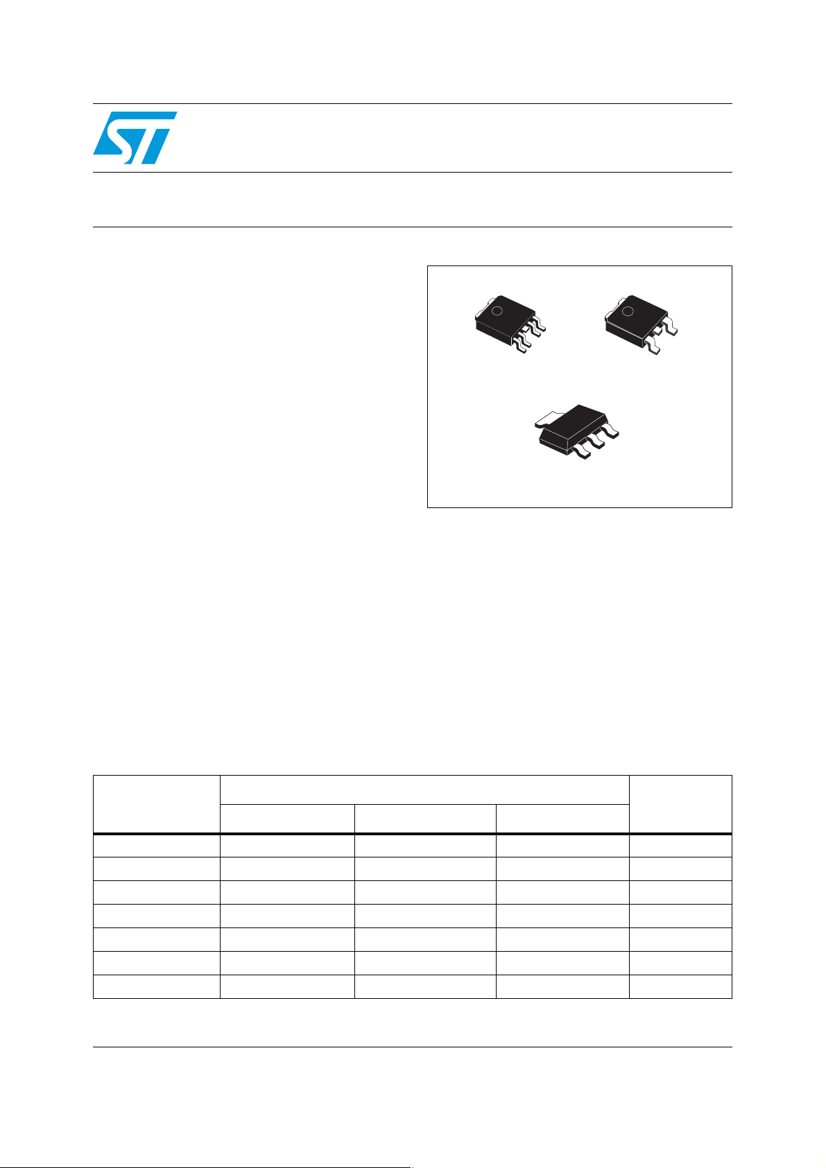
PPAK DPAK
The LD29080xx is a high current, high accuracy,
SOT223
low-dropout voltage regulators series. These
regulators feature 400 mV dropout voltages and
very low ground current. Designed for high
current loads, these devices also find applications
in lower current, extremely low dropout-critical
systems, where their tiny dropout voltage and
ground current values are important attributes.
Typical application are in power supply switching
post regulation, series power supply for monitors,
series power supply for VCRs and TVs, computer
systems and battery powered systems.
Table 1. Device summary
Order codes
Part numbers
DPAK (tape and reel) PPAK (tape and reel) SOT223
LD29080XX15 LD29080DT15R LD29080PT15R 1.5 V
LD29080XX18 LD29080DT18R LD29080PT18R 1.8 V
Output voltages
LD29080XX25 LD29080DT25R LD29080PT25R 2.5 V
LD29080XX33 LD29080DT33R LD29080PT33R LD29080S33R 3.3 V
LD29080XX50 LD29080DT50R LD29080PT50R 5.0 V
LD29080XX90 LD29080DT90R LD29080PT90R 9.0 V
LD29080XX LD29080PTR ADJ
May 2012 Doc ID 10918 Rev 7 1/24
This is information on a product in full production.
www.st.com
24

Contents LD29080xx
Contents
1 Diagram . . . . . . . . . . . . . . . . . . . . . . . . . . . . . . . . . . . . . . . . . . . . . . . . . . . 3
2 Pin configuration . . . . . . . . . . . . . . . . . . . . . . . . . . . . . . . . . . . . . . . . . . . 4
3 Maximum ratings . . . . . . . . . . . . . . . . . . . . . . . . . . . . . . . . . . . . . . . . . . . . 5
4 Electrical characteristics . . . . . . . . . . . . . . . . . . . . . . . . . . . . . . . . . . . . . 6
5 Typical characteristics . . . . . . . . . . . . . . . . . . . . . . . . . . . . . . . . . . . . . . 14
6 Package mechanical data . . . . . . . . . . . . . . . . . . . . . . . . . . . . . . . . . . . . 17
7 Revision history . . . . . . . . . . . . . . . . . . . . . . . . . . . . . . . . . . . . . . . . . . . 23
2/24 Doc ID 10918 Rev 7
LD29080xx Diagram
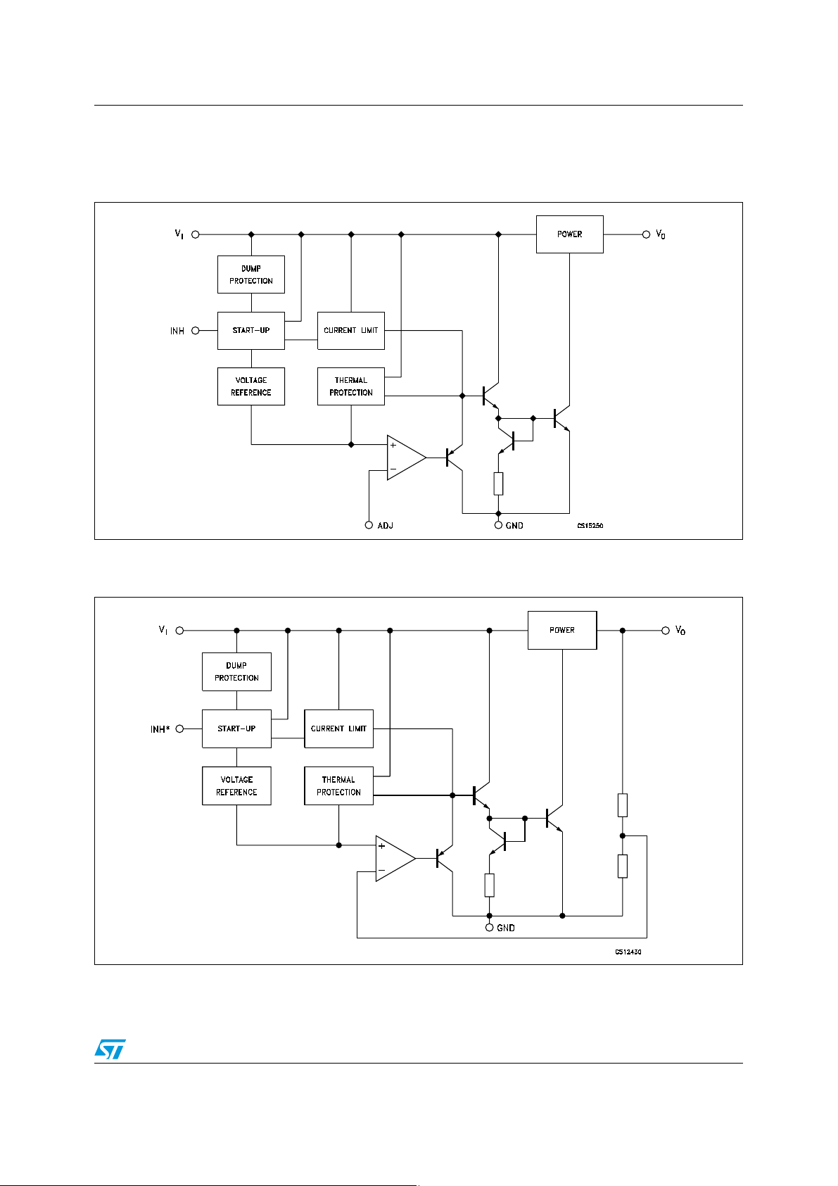
1 Diagram
Figure 1. Schematic diagram for adjustable version
Figure 2. Schematic diagram for fixed version
* Only for version with inhibit function.
Doc ID 10918 Rev 7 3/24
Pin configuration LD29080xx
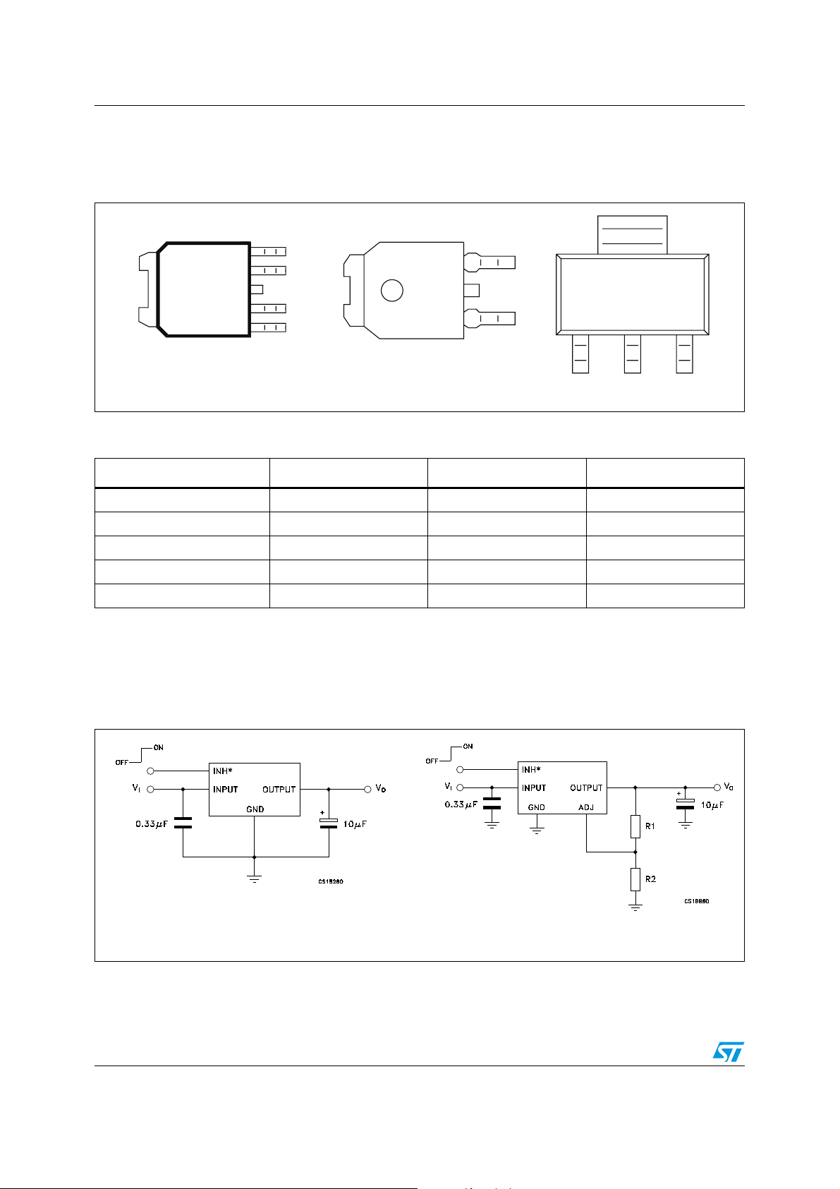
2 Pin configuration
Figure 3. Pin connections (top view)
GND
PPAK
CS17230
5
4
3
GND
2
1
CS17240
DPAK
3
GND
2
1
123
AM09358v1
SOT223
Table 2. Pin description
Symbol PPAK DPAK SOT223
V
I
GND 3 2 2
V
O
ADJ/N.C.
INHIBIT
1. Not connect for fixed version.
2. Not internally pulled up; in order to assure the operating condition (device in ON mode), it must be connected to a positive
voltage higher than 2 V.
(1)
(2)
211
433
5
1
Figure 4. Application circuit
* Only for version with inhibit function.
4/24 Doc ID 10918 Rev 7
VO = V
(1 + R1/R2)
REF
LD29080xx Maximum ratings
3 Maximum ratings
Table 3. Absolute maximum ratings
Symbol Parameter Value Unit
V
I
V
INH
I
O
P
D
T
STG
T
OP
1. Above 14 V the device is automatically in shut-down.
DC input voltage 30
Inhibit input voltage 14 V
Output current Internally limited mA
Power dissipation Internally limited mW
Storage temperature range - 55 to 150 °C
Operating temperature range - 40 to 125 °C
Note: Absolute maximum ratings are those values beyond which damage to the device may occur.
Functional operation under these conditions is not implied.
Table 4. Thermal data
(1)
V
Symbol Parameter DPAK PPAK SOT223 Unit
R
R
thJC
thJA
Thermal resistance junction-case 8 8 25 °C/W
Thermal resistance junction-ambient 100 100 110 °C/W
Doc ID 10918 Rev 7 5/24
Electrical characteristics LD29080xx
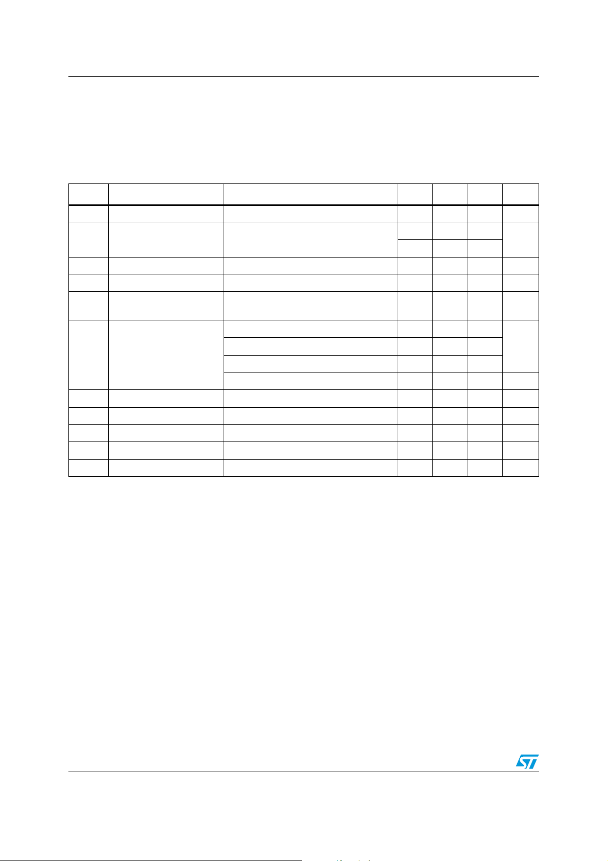
4 Electrical characteristics
IO = 10 mA, (
Note 4
) TJ = 25 °C, VI = 3.5 V, V
= 2V, CI = 330 nF, CO = 10 µF, unless
INH
otherwise specified.
Table 5. Electrical characteristics of LD29080#15
Symbol Parameter Test conditions Min. Typ. Max. Unit
V
I
V
O
ΔV
O
ΔV
O
SVR Supply voltage rejection
I
q
I
sc
V
IL
V
IH
I
INH
eN Output noise voltage BP = 10Hz to 100kHz, IO = 100mA 60 µV
Operating input voltage IO = 10mA to 800mA 2.5 13 V
Output voltage
= 10mA to 800mA, VI = 3 to 7V
I
O
= -40 to 125°C
T
J
1.485 1.5 1.515
1.463 1.537
Load regulation IO = 10mA to 800mA 0.2 1.0 %
Line regulation VI = 3 to 13V 0.06 0.5 %
f = 120 Hz, V
(
Note 1
= 3.8 ± 1V, IO = 400mA
I
)
65 75 dB
IO = 10mA, TJ = -40 to 125°C 2 5
Quiescent current
= 400mA, TJ = -40 to 125°C 8 20
O
mAI
IO = 800mA, TJ = -40 to 125°C 14 35
V
= 13V, V
I
= GND, TJ = -40 to 125°C 130 180 µA
INH
Short circuit current RL = 0 1.2 A
Control input logic low OFF MODE, TJ = -40 to 125°C 0.8 V
Control input logic high ON MODE, TJ = -40 to 125°C 2 V
Control input current V
= 13V, TJ = -40 to 125°C 5 10 µA
INH
V
RMS
Note: 1 Guaranteed by design.
2 Dropout voltage is defined as the input-to-output differential when the output voltage drops
to 99% of its nominal value with V
+ 1 V applied to VI.
O
3 Reference voltage is measured between output and GND pins, with ADJ PIN tied to V
4 In order to avoid any output voltage rise within the whole operating temperature range, due
to output leakage current, a minimum load current of 2 mA is required.
6/24 Doc ID 10918 Rev 7
.
O
LD29080xx Electrical characteristics
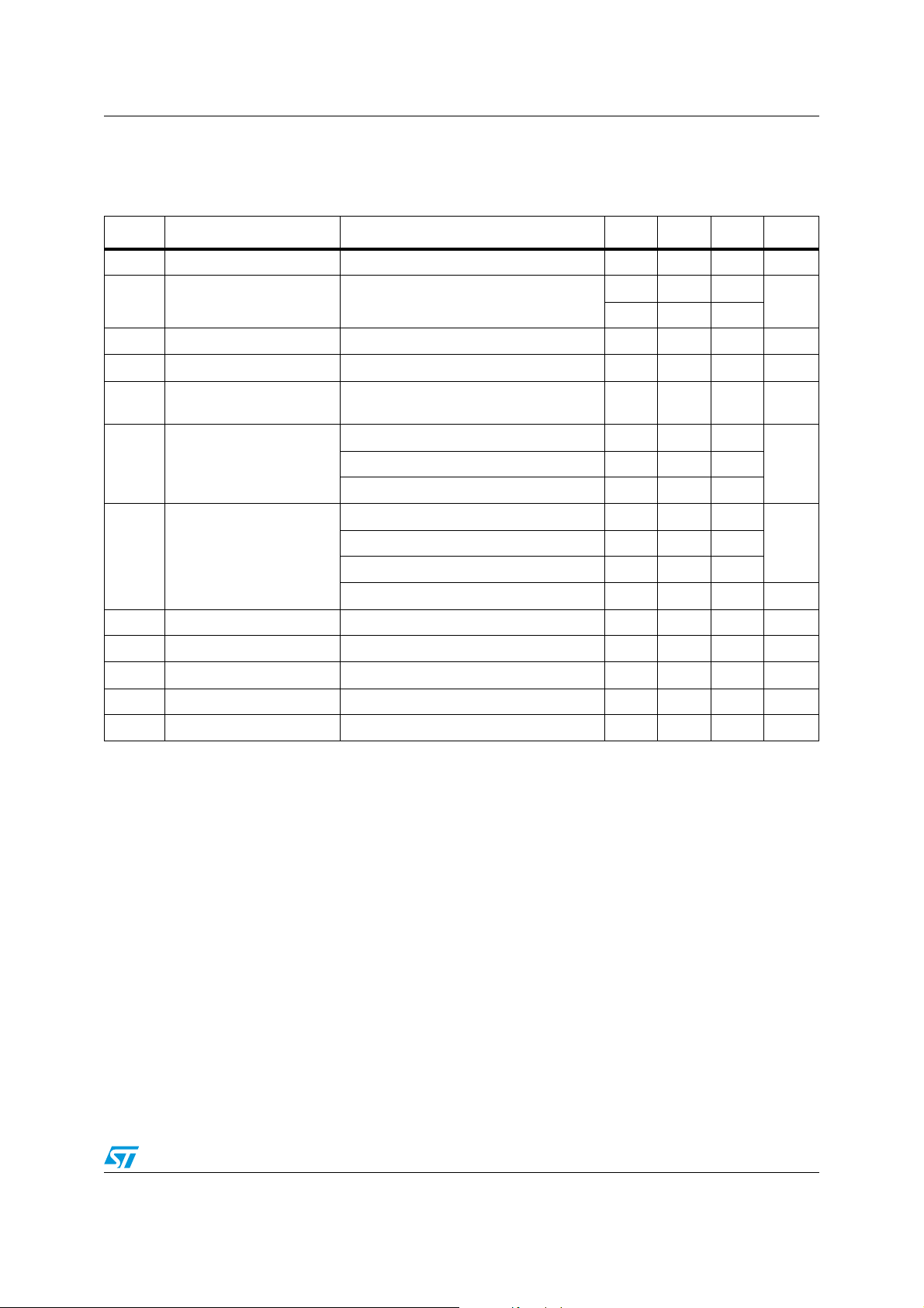
IO = 10 mA, (
Note 4
) TJ = 25 °C, VI = 3.5 V, V
= 2 V, CI = 330 nF, CO = 10 µF, unless
INH
otherwise specified.
Table 6. Electrical characteristics of LD29080#18
Symbol Parameter Test conditions Min. Typ. Max. Unit
V
I
V
O
ΔV
O
ΔV
O
SVR Supply voltage rejection
V
DROP
I
q
I
sc
V
IL
V
IH
I
INH
eN Output noise voltage B
Operating input voltage IO = 10mA to 800mA 2.5 13 V
Output voltage
IO = 10mA to 800mA, VI = 3 to 7.3V
T
= -40 to 125°C
J
1.782 1.8 1.818
1.755 1.845
Load regulation IO = 10mA to 800mA 0.2 1.0 %
Line regulation VI = 3 to 13V 0.06 0.5 %
Dropout voltage
f = 120 Hz, VI = 3.8 ± 1V, IO = 400mA
Note 1
)
(
IO = 150mA, TJ = -40 to 125°C (
Note 2
Note 2
I
= 800mA, TJ = -40 to 125°C (
O
I
= 10mA, TJ = -40 to 125°C 2 5
O
Note 2
62 72 dB
)0.1
)0.2
)0.40.7
mAIO = 400mA, TJ = -40 to 125°C 8 20
Quiescent current
I
= 800mA, TJ = -40 to 125°C 14 35
O
V
= 13V, V
I
= GND, TJ = -40 to 125°C 130 180 µA
INH
Short circuit current RL = 0 1.2 A
Control input logic low OFF MODE, TJ = -40 to 125°C 0.8 V
Control input logic high ON MODE, TJ = -40 to 125°C 2 V
Control input current V
= 13V, TJ = -40 to 125°C 5 10 µA
INH
= 10Hz to 100kHz, IO = 100mA 72 µV
P
V
VIO = 400mA, TJ = -40 to 125°C (
RMS
Note: 1 Guaranteed by design.
2 Dropout voltage is defined as the input-to-output differential when the output voltage drops
to 99% of its nominal value with V
3 Reference voltage is measured between output and GND pins, with ADJ PIN tied to V
4 In order to avoid any output voltage rise within the whole operating temperature range, due
to output leakage current, a minimum load current of 2 mA is required.
+ 1 V applied to VI.
O
.
O
Doc ID 10918 Rev 7 7/24
Electrical characteristics LD29080xx
IO = 10 mA, (
Note 4
) TJ = 25 °C, VI = 4.5 V, V
= 2 V, CI = 330 nF, CO = 10 µF, unless
INH
otherwise specified.
Table 7. Electrical characteristics of LD29080#25
Symbol Parameter Test conditions Min. Typ. Max. Unit
V
I
V
O
ΔV
O
ΔV
O
SVR Supply voltage rejection
V
DROP
I
q
I
sc
V
IL
V
IH
I
INH
eN Output noise voltage B
Operating input voltage IO = 10mA to 800mA 13 V
Output voltage
IO = 10mA to 800mA, VI = 3.5 to 8V
T
= -40 to 125°C
J
2.475 2.5 2.525
2.438 2.562
Load regulation IO = 10mA to 800mA 0.2 1.0 %
Line regulation VI = 3.5 to 13V 0.06 0.5 %
Dropout voltage
f = 120 Hz, VI = 4.5 ± 1V, IO = 400mA
Note 1
)
(
IO = 150mA, TJ = -40 to 125°C (
Note 2
Note 2
I
= 800mA, TJ = -40 to 125°C (
O
I
= 10mA, TJ = -40 to 125°C 2 5
O
Note 2
55 70 dB
)0.1
)0.2
)0.40.7
mAIO = 400mA, TJ = -40 to 125°C 8 20
Quiescent current
I
= 800mA, TJ = -40 to 125°C 14 35
O
V
= 13V, V
I
= GND, TJ = -40 to 125°C 130 180 µA
INH
Short circuit current RL = 0 1.2 A
Control input logic low OFF MODE, TJ = -40 to 125°C 0.8 V
Control input logic high ON MODE, TJ = -40 to 125°C 2 V
Control input current V
= 13V, TJ = -40 to 125°C 5 10 µA
INH
= 10Hz to 100kHz, IO = 100mA 100 µV
P
V
VIO = 400mA, TJ = -40 to 125°C (
RMS
Note: 1 Guaranteed by design.
2 Dropout voltage is defined as the input-to-output differential when the output voltage drops
to 99% of its nominal value with V
+ 1 V applied to VI.
O
3 Reference voltage is measured between output and GND pins, with ADJ PIN tied to V
4 In order to avoid any output voltage rise within the whole operating temperature range, due
to output leakage current, a minimum load current of 2 mA is required.
8/24 Doc ID 10918 Rev 7
.
O
 Loading...