


LD1117AXX12, LD1117AXX18,
Low drop fixed and adjustable positive voltage regulators
Features
■ Low dropout voltage:
– 1.15 V typ. @ I
■ Very low quiescent current:
– 5 mA typ. @ 25 °C
■ Output current up to 1 A
■ Fixed output voltage of:
– 1.2 V, 1.8 V, 2.5 V, 3.3 V
■ Adjustable version availability (V
■ Internal current and thermal limit
■ Only 10 µF for stability
■ Available in ± 2% (at 25 °C) and 4% in full
temperature range
■ High supply voltage rejection:
– 80 dB typ. (at 25 °C)
■ Temperature range: 0 °C to 125 °C
= 1 A, 25 °C
OUT
= 1.25 V)
REF
LD1117AXX33, LD1117AXX
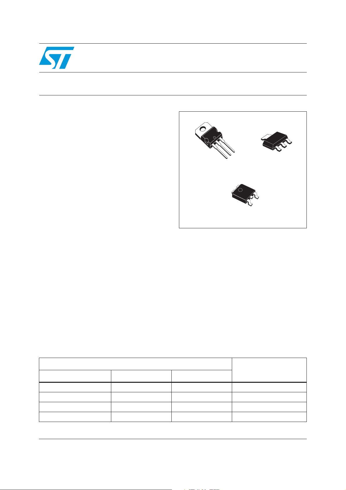
TO-220
DPAK
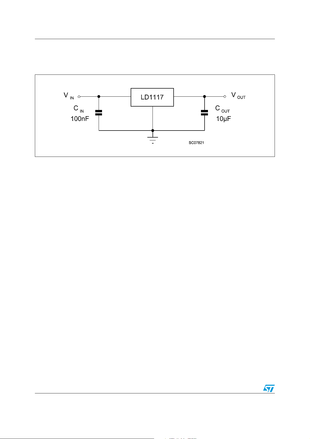
common 10 µF minimum capacitor is needed for
stability. Chip trimming allows the regulator to
reach a very tight output voltage tolerance, within
± 2% at 25 °C.
SOT-223
Description
The LD1117Axx is a low drop voltage regulator
able to provide up to 1 A of output current,
available also in adjustable versions (V
1.25 V). In fixed versions, the following output
voltages are offered: 1.2 V, 1.8 V, 2.5 V and 3.3 V.
The device is supplied in: SOT-223, DPAK and
TO-220. Surface mounted packages optimize the
thermal characteristics while offering a relevant
space saving advantage. High efficiency is
assured by an NPN pass transistor. Only a very
Table 1. Device summary
Order codes
SOT-223 DPAK TO-220
LD1117AS12TR LD1117ADT12TR 1.2 V
LD1117AS18TR LD1117ADT18TR 1.8 V
LD1117AS33TR LD1117ADT33TR LD1117AV33 3.3 V
LD1117ASTR LD1117ADT-TR Adjustable from 1.25 V
December 2011 Doc ID 7194 Rev 24 1/24
REF
=
Output voltage
www.st.com
24

Contents LD1117AXX12, LD1117AXX18, LD1117AXX33, LD1117AXX
Contents
1 Diagram . . . . . . . . . . . . . . . . . . . . . . . . . . . . . . . . . . . . . . . . . . . . . . . . . . . 3
2 Pin configuration . . . . . . . . . . . . . . . . . . . . . . . . . . . . . . . . . . . . . . . . . . . 4
3 Maximum ratings . . . . . . . . . . . . . . . . . . . . . . . . . . . . . . . . . . . . . . . . . . . . 5
4 Schematic application . . . . . . . . . . . . . . . . . . . . . . . . . . . . . . . . . . . . . . . 6
5 Electrical characteristics . . . . . . . . . . . . . . . . . . . . . . . . . . . . . . . . . . . . . 7
6 Typical application . . . . . . . . . . . . . . . . . . . . . . . . . . . . . . . . . . . . . . . . . 11
7 LD1117A adjustable: application note . . . . . . . . . . . . . . . . . . . . . . . . . 14
8 Package mechanical data . . . . . . . . . . . . . . . . . . . . . . . . . . . . . . . . . . . . 15
9 Revision history . . . . . . . . . . . . . . . . . . . . . . . . . . . . . . . . . . . . . . . . . . . 23
2/24 Doc ID 7194 Rev 24
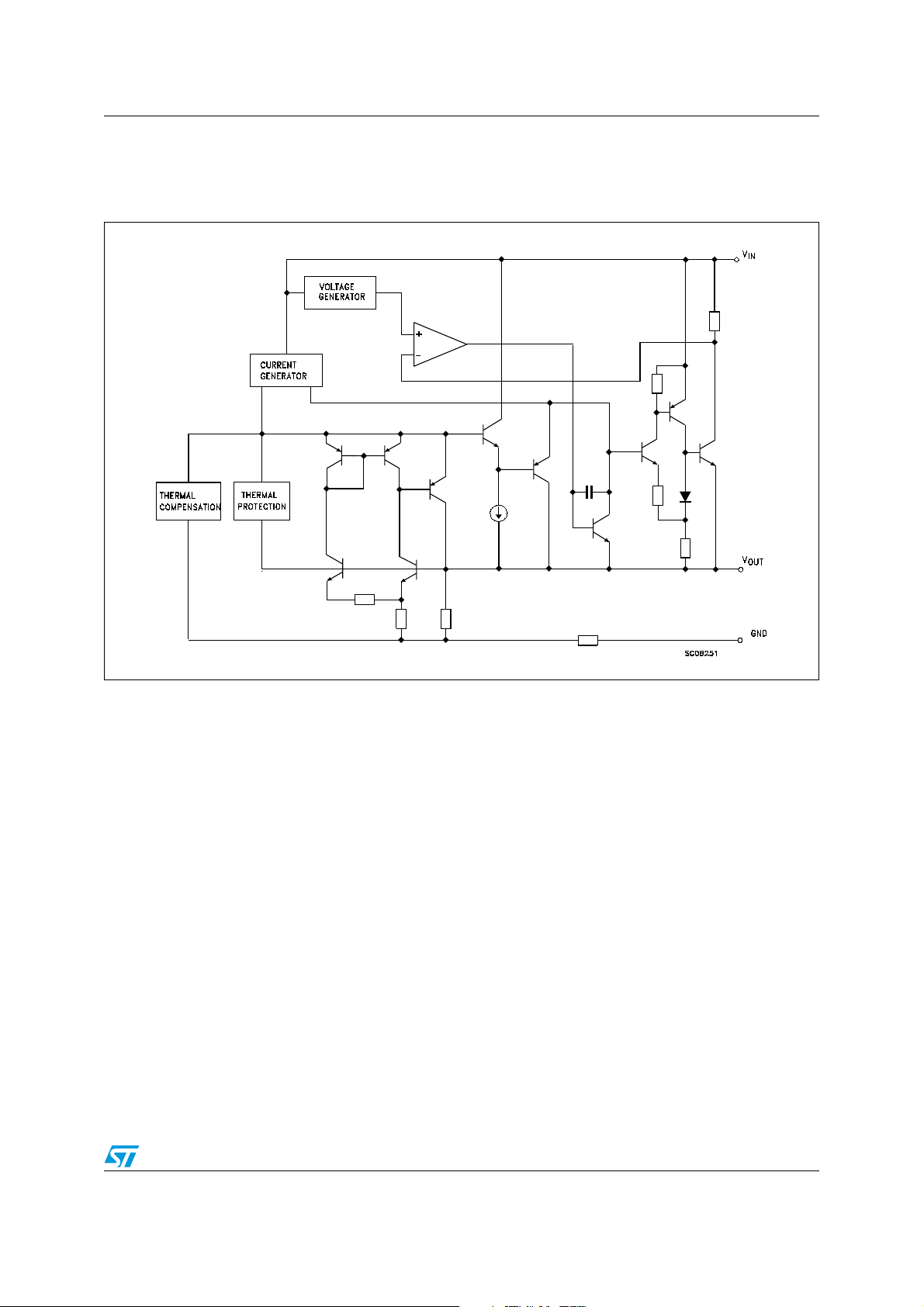
LD1117AXX12, LD1117AXX18, LD1117AXX33, LD1117AXX Diagram
1 Diagram
Figure 1. Block diagram
Doc ID 7194 Rev 24 3/24
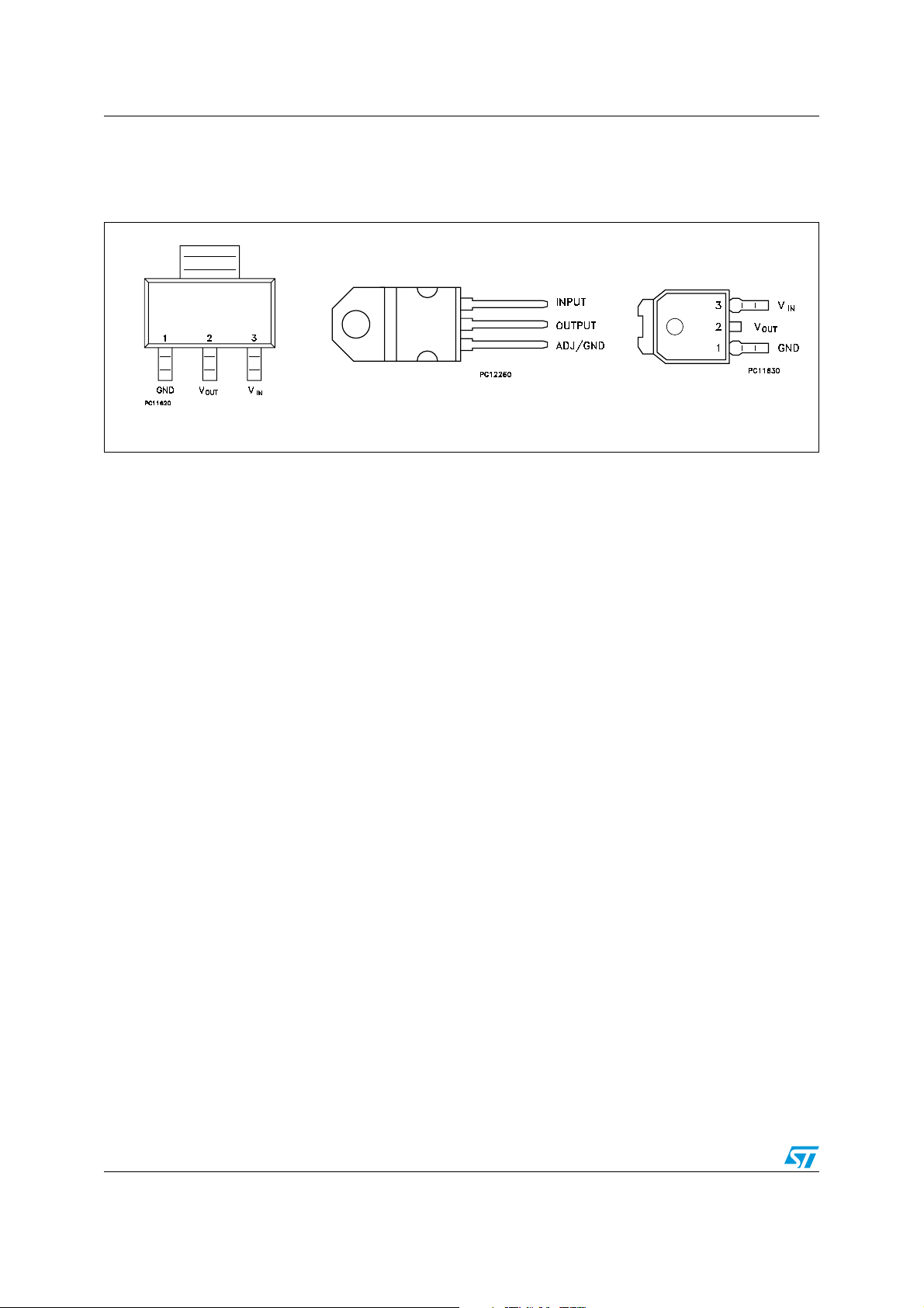
Pin configuration LD1117AXX12, LD1117AXX18, LD1117AXX33, LD1117AXX
2 Pin configuration
Figure 2. Pin connections (top view)
SOT-223
Note: The TAB is connected to the V
OUT
TO-220
.
DPAK
4/24 Doc ID 7194 Rev 24
LD1117AXX12, LD1117AXX18, LD1117AXX33, LD1117AXX Maximum ratings
3 Maximum ratings
Table 2. Absolute maximum ratings
Symbol Parameter Value Unit
T
V
P
STG
T
IN
D
OP
DC input voltage 15 V
Power dissipation 12 W
Storage temperature range -40 to +150 °C
Operating junction temperature range 0 to +125 °C
Note: Absolute maximum ratings are those values beyond which damage to the device may occur.
Functional operation under these condition is not implied. Beyond the above suggested
max. power dissipation, a short-circuit may permanently damage the device.
Table 3. Thermal data
Symbol Parameter SOT-223 DPAK TO-220 Unit
R
R
thJC
thJA
Thermal resistance junction-case 15 8 5 °C/W
Thermal resistance junction-ambient 50 °C/W
Doc ID 7194 Rev 24 5/24
Schematic application LD1117AXX12, LD1117AXX18, LD1117AXX33, LD1117AXX
4 Schematic application
Figure 3. Application circuit (for other fixed output voltages)
6/24 Doc ID 7194 Rev 24
LD1117AXX12, LD1117AXX18, LD1117AXX33, LD1117AXX Electrical characteristics
5 Electrical characteristics
Refer to the test circuits, TJ = 0 to 125 °C, CO = 10 µF, CI = 10 µF, R = 120 Ω between OUTGND, unless otherwise specified.
Table 4. Electrical characteristics of LD1117A#12
Symbol Parameter Test conditions Min. Typ. Max. Unit
V
V
ΔV
ΔV
ΔV
ΔV
Output voltage VI = 5.3 V, IO = 10 mA, TJ = 25 °C 1.176 1.2 1.224 V
O
Output voltage IO = 0 to 1 A, VI = 2.75 to 10 V 1.152 1.2 1.248 V
O
Line regulation VI = 2.75 to 8 V, IO = 0 mA 1 6 mV
O
Load regulation VI = 2.75 V, IO = 0 to 1 A 1 10 mV
O
Temperature stability 0.5 %
O
Long term stability 1000 hrs, TJ = 125 °C 0.3 %
O
Operating input voltage IO = 100 mA 10 V
V
I
I
Quiescent current VI ≤ 8 V, IO = 0 mA 5 10 mA
d
Output current VI - VO = 5 V, TJ = 25 °C 1000 1200 mA
I
O
eN Output noise voltage B =10 Hz to 10 kHz, T
I
= 40 mA, f = 120 Hz
SVR Supply voltage rejection
ΔV
V
O(pwr)
Dropout voltage
D
Thermal regulation Ta = 25 °C, 30 ms pulse 0.08 0.2 %/W
O
VI - VO = 3 V, V
= 100 mA 1 1.10
I
O
= 500 mA 1.05 1.15
O
= 1 A 1.15 1.30
I
O
ripple
= 25 °C 100 µV
J
= 1 V
PP
60 80 dB
VI
Doc ID 7194 Rev 24 7/24
Electrical characteristics LD1117AXX12, LD1117AXX18, LD1117AXX33, LD1117AXX
Refer to the test circuits, TJ = 0 to 125 °C, CO = 10 µF, CI = 10 µF, unless otherwise
specified.
Table 5. Electrical characteristics of LD1117A#18
Symbol Parameter Test conditions Min. Typ. Max. Unit
V
V
ΔV
ΔV
ΔV
ΔV
Output voltage VI = 3.8 V, IO = 10 mA, TJ = 25 °C 1.764 1.8 1.836 V
O
Output voltage IO = 0 to 1 A, VI = 3.3 to 8 V 1.728 1.872 V
O
Line regulation VI = 3.3 to 8 V, IO = 0 mA 1 6 mV
O
Load regulation VI = 3.3 V, IO = 0 to 1 A 1 10 mV
O
Temperature stability 0.5 %
O
Long term stability 1000 hrs, TJ = 125 °C 0.3 %
O
Operating input voltage IO = 100 mA 10 V
V
I
I
Quiescent current VI ≤ 8 V, IO = 0 mA 5 10 mA
d
Output current VI - VO = 5 V, TJ = 25 °C 1000 mA
I
O
eN Output noise voltage B =10 Hz to 10 kHz, T
= 40 mA, f = 120 Hz
I
SVR Supply voltage rejection
Dropout voltage
D
Thermal regulation Ta = 25 °C, 30 ms pulse 0.08 0.2 %/W
ΔV
V
O(pwr)
O
VI - VO = 3 V, V
I
= 100 mA 1 1.10
O
= 500 mA 1.05 1.15
O
= 1 A 1.15 1.30
I
O
ripple
= 25 °C 100 µV
J
= 1 V
PP
60 80 dB
VI
8/24 Doc ID 7194 Rev 24