

ST LD1086V18, LD1086D2T18TR, LD1086DT18TR, LD1086D2T25TR, LD1086DT25TR User Manual
...
1.5 A adjustable and fixed low drop positive voltage regulator
Features
■ Typical dropout: 1.3 V at 1.5 A
■ Three-terminal adjustable or fixed output
voltage: 1.8 V, 2.5 V, 3.3 V, 5 V, 12 V
■ Automotive grade (adjustable V
and DPAK packages only)
■ Output current guaranteed up to 1.5 A
■ Output tolerance: ± 1 % at 25 °C and ± 2 % in
full temperature range
■ Internal power and thermal limit
■ Wide operating temperature range - 40 °C to
125 °C
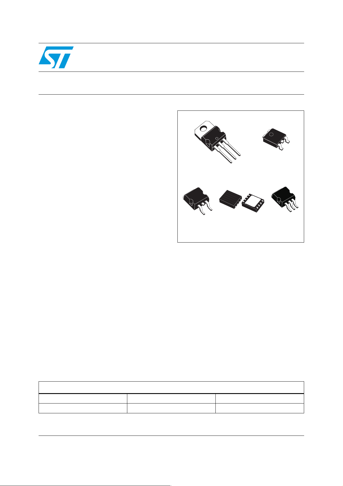
■ Package available: TO-220, D²PAK, D²PAK/A,
DPAK and DFN8 (4x4 mm)
■ Pinout compatibility with standard adjustable
voltage regulators
Description
The LD1086xx is a low drop voltage regulator
capable of providing up to 1.5 A of output current.
Dropout is guaranteed at a maximum of 1.2 V at
the maximum output current, decreasing at lower
loads. The LD1086xx is pin-to-pin compatible with
older 3-terminal adjustable regulators, but has
better performance in terms of drop and output
tolerance. The 2.85 V output version is suitable for
SCSI-2 active terminations. Unlike PNP
regulators, where a part of the output current is
wasted as quiescent current, the LD1086xx
quiescent current flows into the load, increasing
efficiency. Only a 10 µF (minimum) capacitor is
needed for stability. The device is available in a
TO-220, D²PAK, D²PAK/A, DPAK or DFN8 (4x4
in TO-220
OUT
LD1086xx
Datasheet − production data
DPAK
TO-220
D²PAK
DFN8 (4x4)
mm) package. On-chip trimming allows the
regulator to reach a very tight output voltage
tolerance; within ± 1 % at 25 °C. The LD1086xx is
available as automotive grade for adjustable
output voltages in the TO-220 and DPAK
packages. The PAT, SYL, SBL statistical tests
have been performed, and the devices are
qualified according to the AEC-Q100 specification
for the automotive market in the temperature
range of - 40 °C to 125 °C.
D²PAK/A
Table 1. Device summary
Part numbers
LD1086XX LD1086XX18 LD1086XX33
LD1086XX12 LD1086XX25 LD1086XX50
March 2012 Doc ID 6739 Rev 27 1/44
This is information on a product in full production.
www.st.com
44

Contents LD1086xx
Contents
1 Diagram . . . . . . . . . . . . . . . . . . . . . . . . . . . . . . . . . . . . . . . . . . . . . . . . . . . 5
2 Pin configuration . . . . . . . . . . . . . . . . . . . . . . . . . . . . . . . . . . . . . . . . . . . . 6
3 Maximum ratings . . . . . . . . . . . . . . . . . . . . . . . . . . . . . . . . . . . . . . . . . . . . 7
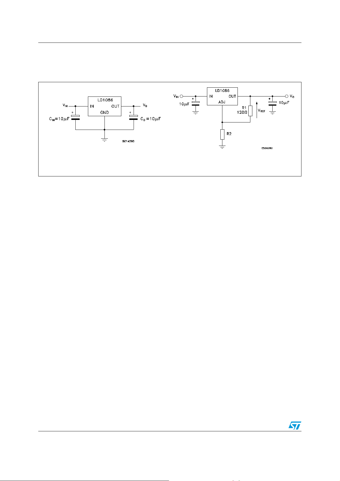
4 Schematic application . . . . . . . . . . . . . . . . . . . . . . . . . . . . . . . . . . . . . . . 8
5 Electrical characteristics . . . . . . . . . . . . . . . . . . . . . . . . . . . . . . . . . . . . . 9
6 Typical application . . . . . . . . . . . . . . . . . . . . . . . . . . . . . . . . . . . . . . . . . 17
7 Package mechanical data . . . . . . . . . . . . . . . . . . . . . . . . . . . . . . . . . . . . 22
8 Order codes . . . . . . . . . . . . . . . . . . . . . . . . . . . . . . . . . . . . . . . . . . . . . . . 42
9 Revision history . . . . . . . . . . . . . . . . . . . . . . . . . . . . . . . . . . . . . . . . . . . 43
2/44 Doc ID 6739 Rev 27

LD1086xx List of tables
List of tables
Table 1. Device summary . . . . . . . . . . . . . . . . . . . . . . . . . . . . . . . . . . . . . . . . . . . . . . . . . . . . . . . . . . 1
Table 2. Absolute maximum ratings . . . . . . . . . . . . . . . . . . . . . . . . . . . . . . . . . . . . . . . . . . . . . . . . . . 7
Table 3. Thermal data. . . . . . . . . . . . . . . . . . . . . . . . . . . . . . . . . . . . . . . . . . . . . . . . . . . . . . . . . . . . . 7
Table 4. Electrical characteristics of LD1086#18 . . . . . . . . . . . . . . . . . . . . . . . . . . . . . . . . . . . . . . . . 9
Table 5. Electrical characteristics of LD1086#25 . . . . . . . . . . . . . . . . . . . . . . . . . . . . . . . . . . . . . . . 10
Table 6. Electrical characteristics of LD1086#33 . . . . . . . . . . . . . . . . . . . . . . . . . . . . . . . . . . . . . . . 11
Table 7. Electrical characteristics of LD1086#36 . . . . . . . . . . . . . . . . . . . . . . . . . . . . . . . . . . . . . . . 12
Table 8. Electrical characteristics of LD1086#50 . . . . . . . . . . . . . . . . . . . . . . . . . . . . . . . . . . . . . . . 13
Table 9. Electrical characteristics of LD1086#12 . . . . . . . . . . . . . . . . . . . . . . . . . . . . . . . . . . . . . . . 14
Table 10. Electrical characteristics of LD1086# . . . . . . . . . . . . . . . . . . . . . . . . . . . . . . . . . . . . . . . . . 15
Table 11. Electrical characteristics of LD1086DTTRY and LD1086VY (Automotive Grade) . . . . . . . 16
Table 12. TO-220 mechanical data . . . . . . . . . . . . . . . . . . . . . . . . . . . . . . . . . . . . . . . . . . . . . . . . . . 22
Table 13. D²PAK mechanical data . . . . . . . . . . . . . . . . . . . . . . . . . . . . . . . . . . . . . . . . . . . . . . . . . . . 29
Table 14. Footprint data . . . . . . . . . . . . . . . . . . . . . . . . . . . . . . . . . . . . . . . . . . . . . . . . . . . . . . . . . . . 30
Table 15. D²PAK/A mechanical data . . . . . . . . . . . . . . . . . . . . . . . . . . . . . . . . . . . . . . . . . . . . . . . . . 33
Table 16. Footprint data . . . . . . . . . . . . . . . . . . . . . . . . . . . . . . . . . . . . . . . . . . . . . . . . . . . . . . . . . . . 34
Table 17. DFN8L (4x4 mm.) mechanical data . . . . . . . . . . . . . . . . . . . . . . . . . . . . . . . . . . . . . . . . . . 35
Table 18. Reel DFN8L dimensions . . . . . . . . . . . . . . . . . . . . . . . . . . . . . . . . . . . . . . . . . . . . . . . . . . . 39
Table 19. Order codes . . . . . . . . . . . . . . . . . . . . . . . . . . . . . . . . . . . . . . . . . . . . . . . . . . . . . . . . . . . . 42
Table 20. Document revision history . . . . . . . . . . . . . . . . . . . . . . . . . . . . . . . . . . . . . . . . . . . . . . . . . 43
Doc ID 6739 Rev 27 3/44

List of figures LD1086xx
List of figures
Figure 1. Schematic diagram . . . . . . . . . . . . . . . . . . . . . . . . . . . . . . . . . . . . . . . . . . . . . . . . . . . . . . . . 5
Figure 2. Pin connections (top view) . . . . . . . . . . . . . . . . . . . . . . . . . . . . . . . . . . . . . . . . . . . . . . . . . . 6
Figure 3. Application circuit . . . . . . . . . . . . . . . . . . . . . . . . . . . . . . . . . . . . . . . . . . . . . . . . . . . . . . . . . 8
Figure 4. Output voltage vs. temp. (V
Figure 5. Output voltage vs. temp. (V
Figure 6. Output voltage vs. temperature (V
Figure 7. Short circuit current vs. dropout voltage . . . . . . . . . . . . . . . . . . . . . . . . . . . . . . . . . . . . . . . 17
Figure 8. Line regulation vs. temperature . . . . . . . . . . . . . . . . . . . . . . . . . . . . . . . . . . . . . . . . . . . . . 17
Figure 9. Load regulation vs. temperature . . . . . . . . . . . . . . . . . . . . . . . . . . . . . . . . . . . . . . . . . . . . . 17
Figure 10. Dropout voltage vs. temperature . . . . . . . . . . . . . . . . . . . . . . . . . . . . . . . . . . . . . . . . . . . . 18
Figure 11. Dropout voltage vs. output current . . . . . . . . . . . . . . . . . . . . . . . . . . . . . . . . . . . . . . . . . . . 18
Figure 12. Adjust pin current vs. input voltage . . . . . . . . . . . . . . . . . . . . . . . . . . . . . . . . . . . . . . . . . . . 18
Figure 13. Adjust pin current vs. temperature . . . . . . . . . . . . . . . . . . . . . . . . . . . . . . . . . . . . . . . . . . . 18
Figure 14. Adjust pin current vs. output current . . . . . . . . . . . . . . . . . . . . . . . . . . . . . . . . . . . . . . . . . . 18
Figure 15. Quiescent current vs. output current. . . . . . . . . . . . . . . . . . . . . . . . . . . . . . . . . . . . . . . . . . 18
Figure 16. Quiescent current vs. input voltage . . . . . . . . . . . . . . . . . . . . . . . . . . . . . . . . . . . . . . . . . . 19
Figure 17. Supply voltage rejection vs. output current. . . . . . . . . . . . . . . . . . . . . . . . . . . . . . . . . . . . . 19
Figure 18. Supply voltage rejection vs. frequency . . . . . . . . . . . . . . . . . . . . . . . . . . . . . . . . . . . . . . . . 19
Figure 19. Supply voltage rejection vs. temperature . . . . . . . . . . . . . . . . . . . . . . . . . . . . . . . . . . . . . . 19
Figure 20. Minimum load current vs. temperature . . . . . . . . . . . . . . . . . . . . . . . . . . . . . . . . . . . . . . . . 19
Figure 21. Stability for adjustable. . . . . . . . . . . . . . . . . . . . . . . . . . . . . . . . . . . . . . . . . . . . . . . . . . . . . 19
Figure 22. Stability for 2.85 V. . . . . . . . . . . . . . . . . . . . . . . . . . . . . . . . . . . . . . . . . . . . . . . . . . . . . . . . 20
Figure 23. Stability for 12 V . . . . . . . . . . . . . . . . . . . . . . . . . . . . . . . . . . . . . . . . . . . . . . . . . . . . . . . . . 20
Figure 24. Line transient (V
Figure 25. Line transient (I
Figure 26. Line transient (C
= 12 to 13 V) . . . . . . . . . . . . . . . . . . . . . . . . . . . . . . . . . . . . . . . . . . . . . . 20
I
= 200 mA) . . . . . . . . . . . . . . . . . . . . . . . . . . . . . . . . . . . . . . . . . . . . . . . . 20
O
= 1 µF) . . . . . . . . . . . . . . . . . . . . . . . . . . . . . . . . . . . . . . . . . . . . . . . . 20
ADJ
Figure 27. Load transient . . . . . . . . . . . . . . . . . . . . . . . . . . . . . . . . . . . . . . . . . . . . . . . . . . . . . . . . . . . 20
Figure 28. Load transient (T
rise
= T
Figure 29. Thermal protection . . . . . . . . . . . . . . . . . . . . . . . . . . . . . . . . . . . . . . . . . . . . . . . . . . . . . . . 21
Figure 30. Drawing dimension TO-220 (type STD-ST Dual Gauge) . . . . . . . . . . . . . . . . . . . . . . . . . . 23
Figure 31. Drawing dimension TO-220 (type STD-ST Single Gauge) . . . . . . . . . . . . . . . . . . . . . . . . . 24
Figure 32. Drawing dimension tube for TO-220 Dual Gauge (mm.) . . . . . . . . . . . . . . . . . . . . . . . . . . 25
Figure 33. Drawing dimension tube for TO-220 Single Gauge (mm.) . . . . . . . . . . . . . . . . . . . . . . . . . 25
Figure 34. Drawing dimension D²PAK (type STD-ST) . . . . . . . . . . . . . . . . . . . . . . . . . . . . . . . . . . . . . 27
Figure 35. Drawing dimension D²PAK (type WOOSEOK-SUBCON.) . . . . . . . . . . . . . . . . . . . . . . . . . 28
Figure 36. D²PAK footprint recommended data . . . . . . . . . . . . . . . . . . . . . . . . . . . . . . . . . . . . . . . . . . 30
Figure 37. Drawing dimension D²PAK/A (type STD-ST) . . . . . . . . . . . . . . . . . . . . . . . . . . . . . . . . . . . 31
Figure 38. Drawing dimension D²PAK/A (type WOOSEOK-Subcon.) . . . . . . . . . . . . . . . . . . . . . . . . . 32
Figure 39. D²PAK/A footprint recommended data . . . . . . . . . . . . . . . . . . . . . . . . . . . . . . . . . . . . . . . . 34
Figure 40. DFN8L package outline . . . . . . . . . . . . . . . . . . . . . . . . . . . . . . . . . . . . . . . . . . . . . . . . . . . 36
Figure 41. DFN8L footprint - recommended data . . . . . . . . . . . . . . . . . . . . . . . . . . . . . . . . . . . . . . . . 37
Figure 42. DFN8L carrier tape (dimension are in mm.) . . . . . . . . . . . . . . . . . . . . . . . . . . . . . . . . . . . . 38
Figure 43. Reel DFN8L drawing . . . . . . . . . . . . . . . . . . . . . . . . . . . . . . . . . . . . . . . . . . . . . . . . . . . . . 39
= 5 V). . . . . . . . . . . . . . . . . . . . . . . . . . . . . . . . . . . . . . . . . . . 17
I
= 15 V). . . . . . . . . . . . . . . . . . . . . . . . . . . . . . . . . . . . . . . . . . 17
I
= 10 µs) . . . . . . . . . . . . . . . . . . . . . . . . . . . . . . . . . . . . . . . . . . 21
fall
= 4.25 V) . . . . . . . . . . . . . . . . . . . . . . . . . . . . . . . . . . . 17
I
4/44 Doc ID 6739 Rev 27
LD1086xx Diagram
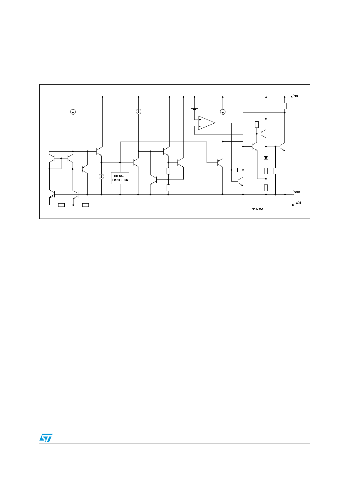
1 Diagram
Figure 1. Schematic diagram
Doc ID 6739 Rev 27 5/44
Pin configuration LD1086xx
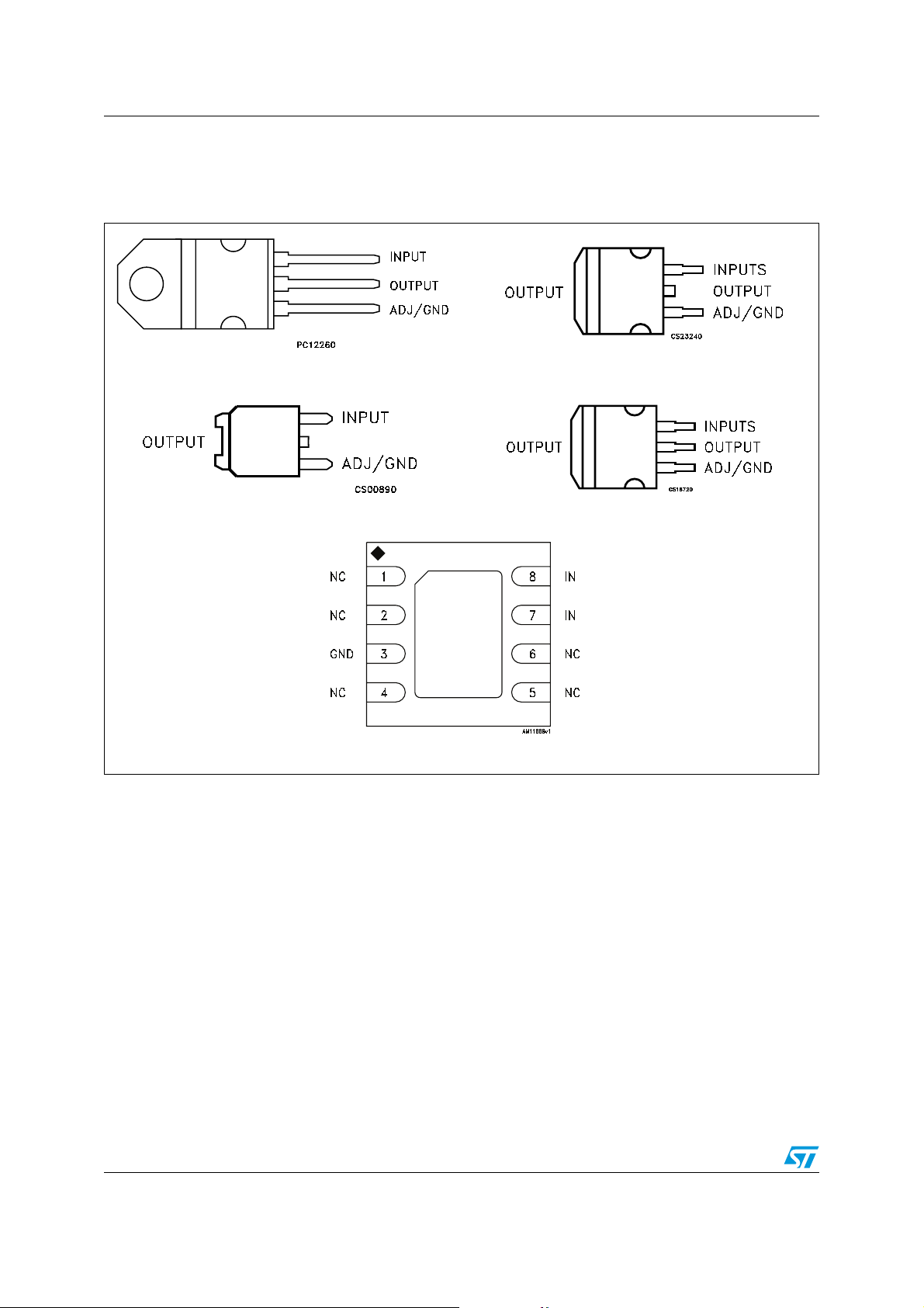
2 Pin configuration
Figure 2. Pin connections (top view)
TO-220
DPAK
OUTPUT
DFN8 (4X4)
D²PAK
D²PAK/A
Note: The TAB is physically connected to the output (this is valid for the TO-220 package too).
6/44 Doc ID 6739 Rev 27
LD1086xx Maximum ratings
3 Maximum ratings
Table 2. Absolute maximum ratings
Symbol Parameter Value Unit
DC input voltage 30 V
Output current Internally Limited mA
Power dissipation Internally Limited mW
Storage temperature range -55 to +150 °C
Operating junction temperature range -40 to +125 °C
T
P
T
V
I
I
O
D
STG
OP
Note: Absolute maximum ratings are those values beyond which damage to the device may occur.
Functional operation under these condition is not implied.
Table 3. Thermal data
Symbol Parameter TO-220
R
R
thJC
thJA
Thermal resistance junction-case 5 3 8 1.5 °C/W
Thermal resistance junction-ambient 50 62.5 33 °C/W
D²PAK
D²PAK/A
DPAK DFN8 Unit
Doc ID 6739 Rev 27 7/44
Schematic application LD1086xx
4 Schematic application
Figure 3. Application circuit
R
2
VOV
⎛⎞
1
⋅=
REF
⎝⎠
------ -+
R
1
8/44 Doc ID 6739 Rev 27
LD1086xx Electrical characteristics
5 Electrical characteristics
VI = 4.8 V, CI = CO =10 µF, TA = -40 to 125 °C, unless otherwise specified.
Table 4. Electrical characteristics of LD1086#18
Symbol Parameter Test condition Min. Typ. Max. Unit
V
ΔV
ΔV
Output voltage
O
Line regulation
O
Load regulation
O
V
Dropout voltage IO = 1.5A 1.3 1.5 V
d
I
Quiescent current VI ≤ 30V 5 10 mA
q
I
Short circuit current
sc
(1)
Thermal regulation T
SVR Supply voltage rejection
RMS Output noise voltage (% of
eN
)
V
O
IO = 0 mA, TJ = 25°C 1.782 1.8 1.818 V
I
= 0 to 1.5A, VI = 3.4 to 30V 1.764 1.8 1.836 V
O
= 0 mA, VI = 3.4 to 18V, TJ = 25°C 0.2 4 mV
I
O
IO = 0 mA, VI = 3.4 to 15V 0.4 4 mV
I
= 0 to 1.5A, TJ = 25°C 0.5 8 mV
O
I
= 0 to 1.5A 1 16 mV
O
V
- VO = 5V 1.5 2 A
I
VI - VO = 25V 0.05 0.02 A
= 25°C, 30ms pulse 0.01 0.04 %/W
A
f = 120 Hz, C
V
= 6.8 ± 3V
I
= 25°C, f =10Hz to 10kHz 0.003 %
T
A
= 25 µF, IO = 1.5A
O
60 82 dB
S Temperature stability 0.5 %
S Long term stability T
1. See short-circuit current curve for available output current at fixed dropout.
= 125°C, 1000Hrs 0.5 %
A
Doc ID 6739 Rev 27 9/44

Electrical characteristics LD1086xx
VI = 5.5 V, CI = CO =10 µF, TA = -40 to 125 °C, unless otherwise specified.
Table 5. Electrical characteristics of LD1086#25
Symbol Parameter Test condition Min. Typ. Max. Unit
V
ΔV
ΔV
Output voltage
O
Line regulation
O
Load regulation
O
V
Dropout voltage IO = 1.5A 1.3 1.5 V
d
I
Quiescent current VI ≤ 30V 5 10 mA
q
Short circuit current
I
sc
(1)
Thermal regulation T
SVR Supply voltage rejection
RMS Output noise voltage (% of
eN
)
V
O
IO = 0 mA, TJ = 25°C 2.475 2.5 2.525 V
I
= 0 to 1.5A, VI = 4.1 to 30V 2.45 2.5 2.55 V
O
I
= 0 mA, VI = 4.1 to 18V, TJ = 25°C 0.2 4 mV
O
I
= 0 mA, VI = 4.1 to 18V 0.4 4 mV
O
= 0 to 1.5A, TJ = 25°C 0.5 8 mV
I
O
IO = 0 to 1.5A 1 16 mV
V
- VO = 5V 1.5 2 A
I
V
- VO = 25V 0.05 0.2 A
I
= 25°C, 30ms pulse 0.008 0.04 %/W
A
f = 120 Hz, CO = 25 µF, IO = 1.5A
= 7.5 ± 3V
V
I
60 81 dB
TA = 25°C, f =10Hz to 10kHz 0.003 %
S Temperature stability 0.5 %
S Long term stability T
1. See short-circuit current curve for available output current at fixed dropout.
= 125°C, 1000Hrs 0.5 %
A
10/44 Doc ID 6739 Rev 27

LD1086xx Electrical characteristics
VI = 6.3 V, CI = CO =10 µF, TA = -40 to 125 °C, unless otherwise specified.
Table 6. Electrical characteristics of LD1086#33
Symbol Parameter Test condition Min. Typ. Max. Unit
V
ΔV
ΔV
Output voltage
O
Line regulation
O
Load regulation
O
V
Dropout voltage IO = 1.5A 1.3 1.5 V
d
I
Quiescent current VI ≤ 30V 5 10 mA
q
Short circuit current
I
sc
(1)
Thermal regulation T
SVR Supply voltage rejection
RMS Output noise voltage (% of
eN
)
V
O
IO = 0 mA, TJ = 25°C 3.267 3.3 3.333 V
I
= 0 to 1.5A, VI = 4.9 to 30V 3.234 3.3 3.366 V
O
I
= 0 mA, VI = 4.9 to 18V, TJ = 25°C 0.5 6 mV
O
I
= 0 mA, VI = 4.9 to 18V 1 6 mV
O
= 0 to 1.5A, TJ = 25°C 1 10 mV
I
O
IO = 0 to 1.5A 7 25 mV
V
- VO = 5V 1.5 2 A
I
V
- VO = 25V 0.05 0.2 A
I
= 25°C, 30ms pulse 0.008 0.04 %/W
A
f = 120 Hz, CO = 25 µF, IO = 1.5A
= 8.3 ± 3V
V
I
60 79 dB
TA = 25°C, f =10Hz to 10kHz 0.003 %
S Temperature stability 0.5 %
S Long term stability T
1. See short-circuit current curve for available output current at fixed dropout.
= 125°C, 1000Hrs 0.5 %
A
Doc ID 6739 Rev 27 11/44
Electrical characteristics LD1086xx
VI = 6.6 V, CI = CO =10 µF, TA = -40 to 125 °C, unless otherwise specified.
Table 7. Electrical characteristics of LD1086#36
Symbol Parameter Test condition Min. Typ. Max. Unit
V
ΔV
ΔV
Output voltage
O
Line regulation
O
Load regulation
O
V
Dropout voltage IO = 1.5A 1.3 1.5 V
d
I
Quiescent current VI ≤ 30V 5 10 mA
q
Short circuit current
I
sc
(1)
Thermal regulation T
SVR Supply voltage rejection
RMS Output noise voltage (% of
eN
)
V
O
IO = 0 mA, TJ = 25°C 3.564 3.6 3.636 V
I
= 0 to 1.5A, VI = 5.2 to 30V 3.528 3.6 3.672 V
O
I
= 0 mA, VI = 5.2 to 18V, TJ = 25°C 0.5 10 mV
O
I
= 0 mA, VI = 5.2 to 18V 1 10 mV
O
= 0 to 1.5A, TJ = 25°C 3 15 mV
I
O
IO = 0 to 1.5A 7 25 mV
V
- VO = 5V 1.5 2 A
I
V
- VO = 25V 0.05 0.2 A
I
= 25°C, 30ms pulse 0.01 0.04 %/W
A
f = 120 Hz, CO = 25 µF, IO = 1.5A
= 8.6 ± 3V
V
I
60 78 dB
TA = 25°C, f =10Hz to 10kHz 0.003 %
S Temperature stability 0.5 %
S Long term stability T
1. See short-circuit current curve for available output current at fixed dropout.
= 125°C, 1000Hrs 0.5 %
A
12/44 Doc ID 6739 Rev 27
LD1086xx Electrical characteristics
VI = 8 V, CI = CO =10 µF, TA = -40 to 125 °C, unless otherwise specified.
Table 8. Electrical characteristics of LD1086#50
Symbol Parameter Test condition Min. Typ. Max. Unit
V
ΔV
ΔV
Output voltage
O
Line regulation
O
Load regulation
O
V
Dropout voltage IO = 1.5A 1.3 1.5 V
d
I
Quiescent current VI ≤ 30V 5 10 mA
q
Short circuit current
I
sc
(1)
Thermal regulation T
SVR Supply voltage rejection
RMS Output noise voltage (% of
eN
)
V
O
IO = 0 mA, TJ = 25°C 4.95 5 5.05 V
I
= 0 to 1.5A, VI = 6.6 to 30V 4.9 5 5.1 V
O
I
= 0 mA, VI = 6.6 to 20V, TJ = 25°C 0.5 10 mV
O
I
= 0 mA, VI = 6.6 to 20V 1 10 mV
O
= 0 to 1.5A, TJ = 25°C 5 20 mV
I
O
IO = 0 to 1.5A 10 35 mV
V
- VO = 5V 1.5 2 A
I
V
- VO = 25V 0.05 0.2 A
I
= 25°C, 30ms pulse 0.01 0.04 %/W
A
f = 120 Hz, CO = 25 µF, IO = 1.5A
= 10 ± 3V
V
I
60 75 dB
TA = 25°C, f =10Hz to 10kHz 0.003 %
S Temperature stability 0.5 %
S Long term stability T
1. See short-circuit current curve for available output current at fixed dropout.
= 125°C, 1000Hrs 0.5 %
A
Doc ID 6739 Rev 27 13/44

Electrical characteristics LD1086xx
VI = 15 V, CI = CO =10 µF, TA = -40 to 125 °C, unless otherwise specified.
Table 9. Electrical characteristics of LD1086#12
Symbol Parameter Test condition Min. Typ. Max. Unit
V
ΔV
ΔV
Output voltage
O
Line regulation
O
Load regulation
O
V
Dropout voltage IO = 1.5A 1.3 1.5 V
d
I
Quiescent current VI ≤ 30V 5 10 mA
q
I
Short circuit current
sc
(1)
IO = 0 mA, TJ = 25°C 11.88 12 12.12 V
I
= 0 to 1.5A, VI = 13.8 to 30V 11.76 12 12.24 V
O
IO = 0 mA, VI = 13.8 to 25V,
= 25°C
T
J
= 0 mA, VI = 13.8 to 25V 2 25 mV
I
O
I
= 0 to 1.5A, TJ = 25°C 12 36 mV
O
I
= 0 to 1.5A 24 72 mV
O
V
- VO = 5V 1.5 2 A
I
V
- VO = 25V 0.05 0.2 A
I
125mV
Thermal regulation TA = 25°C, 30ms pulse 0.01 0.04 %/W
SVR Supply voltage rejection
RMS Output noise voltage (% of
eN
)
V
O
f = 120 Hz, C
= 17 ± 3V
V
I
= 25°C, f =10Hz to 10kHz 0.003 %
T
A
= 25 µF, IO = 1.5A
O
54 66 dB
S Temperature stability 0.5 %
S Long term stability T
1. See short-circuit current curve for available output current at fixed dropout.
= 125°C, 1000Hrs 0.5 %
A
14/44 Doc ID 6739 Rev 27
 Loading...