

1.5 A adjustable and fixed low drop positive voltage regulator
Features
■ Typical dropout: 1.3 V at 1.5 A
■ Three-terminal adjustable or fixed output
voltage: 1.8 V, 2.5 V, 3.3 V, 5 V, 12 V
■ Automotive grade (adjustable V
and DPAK packages only)
■ Output current guaranteed up to 1.5 A
■ Output tolerance: ± 1 % at 25 °C and ± 2 % in
full temperature range
■ Internal power and thermal limit
■ Wide operating temperature range - 40 °C to
125 °C
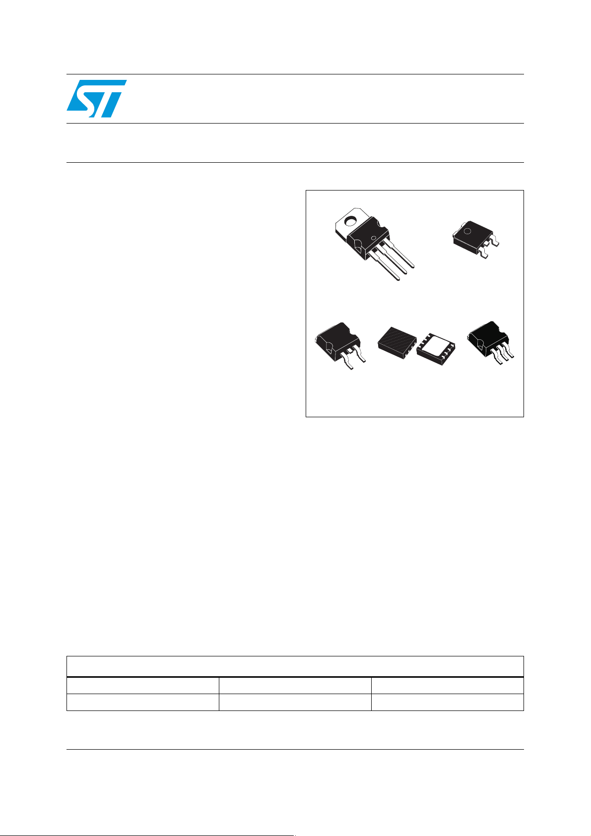
■ Package available: TO-220, D²PAK, D²PAK/A,
DPAK and DFN8 (4x4 mm)
■ Pinout compatibility with standard adjustable
voltage regulators
Description
The LD1086xx is a low drop voltage regulator
capable of providing up to 1.5 A of output current.
Dropout is guaranteed at a maximum of 1.2 V at
the maximum output current, decreasing at lower
loads. The LD1086xx is pin-to-pin compatible with
older 3-terminal adjustable regulators, but has
better performance in terms of drop and output
tolerance. The 2.85 V output version is suitable for
SCSI-2 active terminations. Unlike PNP
regulators, where a part of the output current is
wasted as quiescent current, the LD1086xx
quiescent current flows into the load, increasing
efficiency. Only a 10 µF (minimum) capacitor is
needed for stability. The device is available in a
TO-220, D²PAK, D²PAK/A, DPAK or DFN8 (4x4
in TO-220
OUT
LD1086xx
Datasheet − production data
DPAK
TO-220
D²PAK
DFN8 (4x4)
mm) package. On-chip trimming allows the
regulator to reach a very tight output voltage
tolerance; within ± 1 % at 25 °C. The LD1086xx is
available as automotive grade for adjustable
output voltages in the TO-220 and DPAK
packages. The PAT, SYL, SBL statistical tests
have been performed, and the devices are
qualified according to the AEC-Q100 specification
for the automotive market in the temperature
range of - 40 °C to 125 °C.
D²PAK/A
Table 1. Device summary
Part numbers
LD1086XX LD1086XX18 LD1086XX33
LD1086XX12 LD1086XX25 LD1086XX50
March 2012 Doc ID 6739 Rev 27 1/44
This is information on a product in full production.
www.st.com
44

Contents LD1086xx
Contents
1 Diagram . . . . . . . . . . . . . . . . . . . . . . . . . . . . . . . . . . . . . . . . . . . . . . . . . . . 5
2 Pin configuration . . . . . . . . . . . . . . . . . . . . . . . . . . . . . . . . . . . . . . . . . . . . 6
3 Maximum ratings . . . . . . . . . . . . . . . . . . . . . . . . . . . . . . . . . . . . . . . . . . . . 7
4 Schematic application . . . . . . . . . . . . . . . . . . . . . . . . . . . . . . . . . . . . . . . 8
5 Electrical characteristics . . . . . . . . . . . . . . . . . . . . . . . . . . . . . . . . . . . . . 9
6 Typical application . . . . . . . . . . . . . . . . . . . . . . . . . . . . . . . . . . . . . . . . . 17
7 Package mechanical data . . . . . . . . . . . . . . . . . . . . . . . . . . . . . . . . . . . . 22
8 Order codes . . . . . . . . . . . . . . . . . . . . . . . . . . . . . . . . . . . . . . . . . . . . . . . 42
9 Revision history . . . . . . . . . . . . . . . . . . . . . . . . . . . . . . . . . . . . . . . . . . . 43
2/44 Doc ID 6739 Rev 27

LD1086xx List of tables
List of tables
Table 1. Device summary . . . . . . . . . . . . . . . . . . . . . . . . . . . . . . . . . . . . . . . . . . . . . . . . . . . . . . . . . . 1
Table 2. Absolute maximum ratings . . . . . . . . . . . . . . . . . . . . . . . . . . . . . . . . . . . . . . . . . . . . . . . . . . 7
Table 3. Thermal data. . . . . . . . . . . . . . . . . . . . . . . . . . . . . . . . . . . . . . . . . . . . . . . . . . . . . . . . . . . . . 7
Table 4. Electrical characteristics of LD1086#18 . . . . . . . . . . . . . . . . . . . . . . . . . . . . . . . . . . . . . . . . 9
Table 5. Electrical characteristics of LD1086#25 . . . . . . . . . . . . . . . . . . . . . . . . . . . . . . . . . . . . . . . 10
Table 6. Electrical characteristics of LD1086#33 . . . . . . . . . . . . . . . . . . . . . . . . . . . . . . . . . . . . . . . 11
Table 7. Electrical characteristics of LD1086#36 . . . . . . . . . . . . . . . . . . . . . . . . . . . . . . . . . . . . . . . 12
Table 8. Electrical characteristics of LD1086#50 . . . . . . . . . . . . . . . . . . . . . . . . . . . . . . . . . . . . . . . 13
Table 9. Electrical characteristics of LD1086#12 . . . . . . . . . . . . . . . . . . . . . . . . . . . . . . . . . . . . . . . 14
Table 10. Electrical characteristics of LD1086# . . . . . . . . . . . . . . . . . . . . . . . . . . . . . . . . . . . . . . . . . 15
Table 11. Electrical characteristics of LD1086DTTRY and LD1086VY (Automotive Grade) . . . . . . . 16
Table 12. TO-220 mechanical data . . . . . . . . . . . . . . . . . . . . . . . . . . . . . . . . . . . . . . . . . . . . . . . . . . 22
Table 13. D²PAK mechanical data . . . . . . . . . . . . . . . . . . . . . . . . . . . . . . . . . . . . . . . . . . . . . . . . . . . 29
Table 14. Footprint data . . . . . . . . . . . . . . . . . . . . . . . . . . . . . . . . . . . . . . . . . . . . . . . . . . . . . . . . . . . 30
Table 15. D²PAK/A mechanical data . . . . . . . . . . . . . . . . . . . . . . . . . . . . . . . . . . . . . . . . . . . . . . . . . 33
Table 16. Footprint data . . . . . . . . . . . . . . . . . . . . . . . . . . . . . . . . . . . . . . . . . . . . . . . . . . . . . . . . . . . 34
Table 17. DFN8L (4x4 mm.) mechanical data . . . . . . . . . . . . . . . . . . . . . . . . . . . . . . . . . . . . . . . . . . 35
Table 18. Reel DFN8L dimensions . . . . . . . . . . . . . . . . . . . . . . . . . . . . . . . . . . . . . . . . . . . . . . . . . . . 39
Table 19. Order codes . . . . . . . . . . . . . . . . . . . . . . . . . . . . . . . . . . . . . . . . . . . . . . . . . . . . . . . . . . . . 42
Table 20. Document revision history . . . . . . . . . . . . . . . . . . . . . . . . . . . . . . . . . . . . . . . . . . . . . . . . . 43
Doc ID 6739 Rev 27 3/44

List of figures LD1086xx
List of figures
Figure 1. Schematic diagram . . . . . . . . . . . . . . . . . . . . . . . . . . . . . . . . . . . . . . . . . . . . . . . . . . . . . . . . 5
Figure 2. Pin connections (top view) . . . . . . . . . . . . . . . . . . . . . . . . . . . . . . . . . . . . . . . . . . . . . . . . . . 6
Figure 3. Application circuit . . . . . . . . . . . . . . . . . . . . . . . . . . . . . . . . . . . . . . . . . . . . . . . . . . . . . . . . . 8
Figure 4. Output voltage vs. temp. (V
Figure 5. Output voltage vs. temp. (V
Figure 6. Output voltage vs. temperature (V
Figure 7. Short circuit current vs. dropout voltage . . . . . . . . . . . . . . . . . . . . . . . . . . . . . . . . . . . . . . . 17
Figure 8. Line regulation vs. temperature . . . . . . . . . . . . . . . . . . . . . . . . . . . . . . . . . . . . . . . . . . . . . 17
Figure 9. Load regulation vs. temperature . . . . . . . . . . . . . . . . . . . . . . . . . . . . . . . . . . . . . . . . . . . . . 17
Figure 10. Dropout voltage vs. temperature . . . . . . . . . . . . . . . . . . . . . . . . . . . . . . . . . . . . . . . . . . . . 18
Figure 11. Dropout voltage vs. output current . . . . . . . . . . . . . . . . . . . . . . . . . . . . . . . . . . . . . . . . . . . 18
Figure 12. Adjust pin current vs. input voltage . . . . . . . . . . . . . . . . . . . . . . . . . . . . . . . . . . . . . . . . . . . 18
Figure 13. Adjust pin current vs. temperature . . . . . . . . . . . . . . . . . . . . . . . . . . . . . . . . . . . . . . . . . . . 18
Figure 14. Adjust pin current vs. output current . . . . . . . . . . . . . . . . . . . . . . . . . . . . . . . . . . . . . . . . . . 18
Figure 15. Quiescent current vs. output current. . . . . . . . . . . . . . . . . . . . . . . . . . . . . . . . . . . . . . . . . . 18
Figure 16. Quiescent current vs. input voltage . . . . . . . . . . . . . . . . . . . . . . . . . . . . . . . . . . . . . . . . . . 19
Figure 17. Supply voltage rejection vs. output current. . . . . . . . . . . . . . . . . . . . . . . . . . . . . . . . . . . . . 19
Figure 18. Supply voltage rejection vs. frequency . . . . . . . . . . . . . . . . . . . . . . . . . . . . . . . . . . . . . . . . 19
Figure 19. Supply voltage rejection vs. temperature . . . . . . . . . . . . . . . . . . . . . . . . . . . . . . . . . . . . . . 19
Figure 20. Minimum load current vs. temperature . . . . . . . . . . . . . . . . . . . . . . . . . . . . . . . . . . . . . . . . 19
Figure 21. Stability for adjustable. . . . . . . . . . . . . . . . . . . . . . . . . . . . . . . . . . . . . . . . . . . . . . . . . . . . . 19
Figure 22. Stability for 2.85 V. . . . . . . . . . . . . . . . . . . . . . . . . . . . . . . . . . . . . . . . . . . . . . . . . . . . . . . . 20
Figure 23. Stability for 12 V . . . . . . . . . . . . . . . . . . . . . . . . . . . . . . . . . . . . . . . . . . . . . . . . . . . . . . . . . 20
Figure 24. Line transient (V
Figure 25. Line transient (I
Figure 26. Line transient (C
= 12 to 13 V) . . . . . . . . . . . . . . . . . . . . . . . . . . . . . . . . . . . . . . . . . . . . . . 20
I
= 200 mA) . . . . . . . . . . . . . . . . . . . . . . . . . . . . . . . . . . . . . . . . . . . . . . . . 20
O
= 1 µF) . . . . . . . . . . . . . . . . . . . . . . . . . . . . . . . . . . . . . . . . . . . . . . . . 20
ADJ
Figure 27. Load transient . . . . . . . . . . . . . . . . . . . . . . . . . . . . . . . . . . . . . . . . . . . . . . . . . . . . . . . . . . . 20
Figure 28. Load transient (T
rise
= T
Figure 29. Thermal protection . . . . . . . . . . . . . . . . . . . . . . . . . . . . . . . . . . . . . . . . . . . . . . . . . . . . . . . 21
Figure 30. Drawing dimension TO-220 (type STD-ST Dual Gauge) . . . . . . . . . . . . . . . . . . . . . . . . . . 23
Figure 31. Drawing dimension TO-220 (type STD-ST Single Gauge) . . . . . . . . . . . . . . . . . . . . . . . . . 24
Figure 32. Drawing dimension tube for TO-220 Dual Gauge (mm.) . . . . . . . . . . . . . . . . . . . . . . . . . . 25
Figure 33. Drawing dimension tube for TO-220 Single Gauge (mm.) . . . . . . . . . . . . . . . . . . . . . . . . . 25
Figure 34. Drawing dimension D²PAK (type STD-ST) . . . . . . . . . . . . . . . . . . . . . . . . . . . . . . . . . . . . . 27
Figure 35. Drawing dimension D²PAK (type WOOSEOK-SUBCON.) . . . . . . . . . . . . . . . . . . . . . . . . . 28
Figure 36. D²PAK footprint recommended data . . . . . . . . . . . . . . . . . . . . . . . . . . . . . . . . . . . . . . . . . . 30
Figure 37. Drawing dimension D²PAK/A (type STD-ST) . . . . . . . . . . . . . . . . . . . . . . . . . . . . . . . . . . . 31
Figure 38. Drawing dimension D²PAK/A (type WOOSEOK-Subcon.) . . . . . . . . . . . . . . . . . . . . . . . . . 32
Figure 39. D²PAK/A footprint recommended data . . . . . . . . . . . . . . . . . . . . . . . . . . . . . . . . . . . . . . . . 34
Figure 40. DFN8L package outline . . . . . . . . . . . . . . . . . . . . . . . . . . . . . . . . . . . . . . . . . . . . . . . . . . . 36
Figure 41. DFN8L footprint - recommended data . . . . . . . . . . . . . . . . . . . . . . . . . . . . . . . . . . . . . . . . 37
Figure 42. DFN8L carrier tape (dimension are in mm.) . . . . . . . . . . . . . . . . . . . . . . . . . . . . . . . . . . . . 38
Figure 43. Reel DFN8L drawing . . . . . . . . . . . . . . . . . . . . . . . . . . . . . . . . . . . . . . . . . . . . . . . . . . . . . 39
= 5 V). . . . . . . . . . . . . . . . . . . . . . . . . . . . . . . . . . . . . . . . . . . 17
I
= 15 V). . . . . . . . . . . . . . . . . . . . . . . . . . . . . . . . . . . . . . . . . . 17
I
= 10 µs) . . . . . . . . . . . . . . . . . . . . . . . . . . . . . . . . . . . . . . . . . . 21
fall
= 4.25 V) . . . . . . . . . . . . . . . . . . . . . . . . . . . . . . . . . . . 17
I
4/44 Doc ID 6739 Rev 27
LD1086xx Diagram
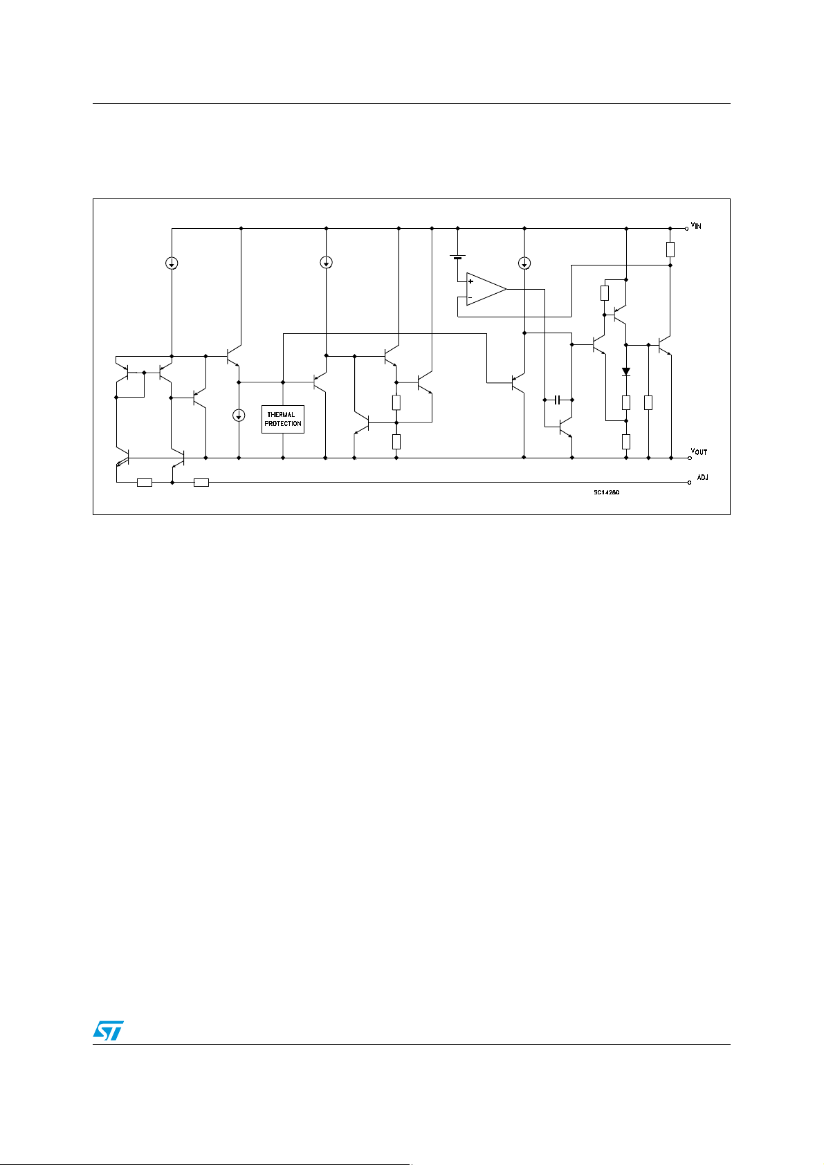
1 Diagram
Figure 1. Schematic diagram
Doc ID 6739 Rev 27 5/44
Pin configuration LD1086xx
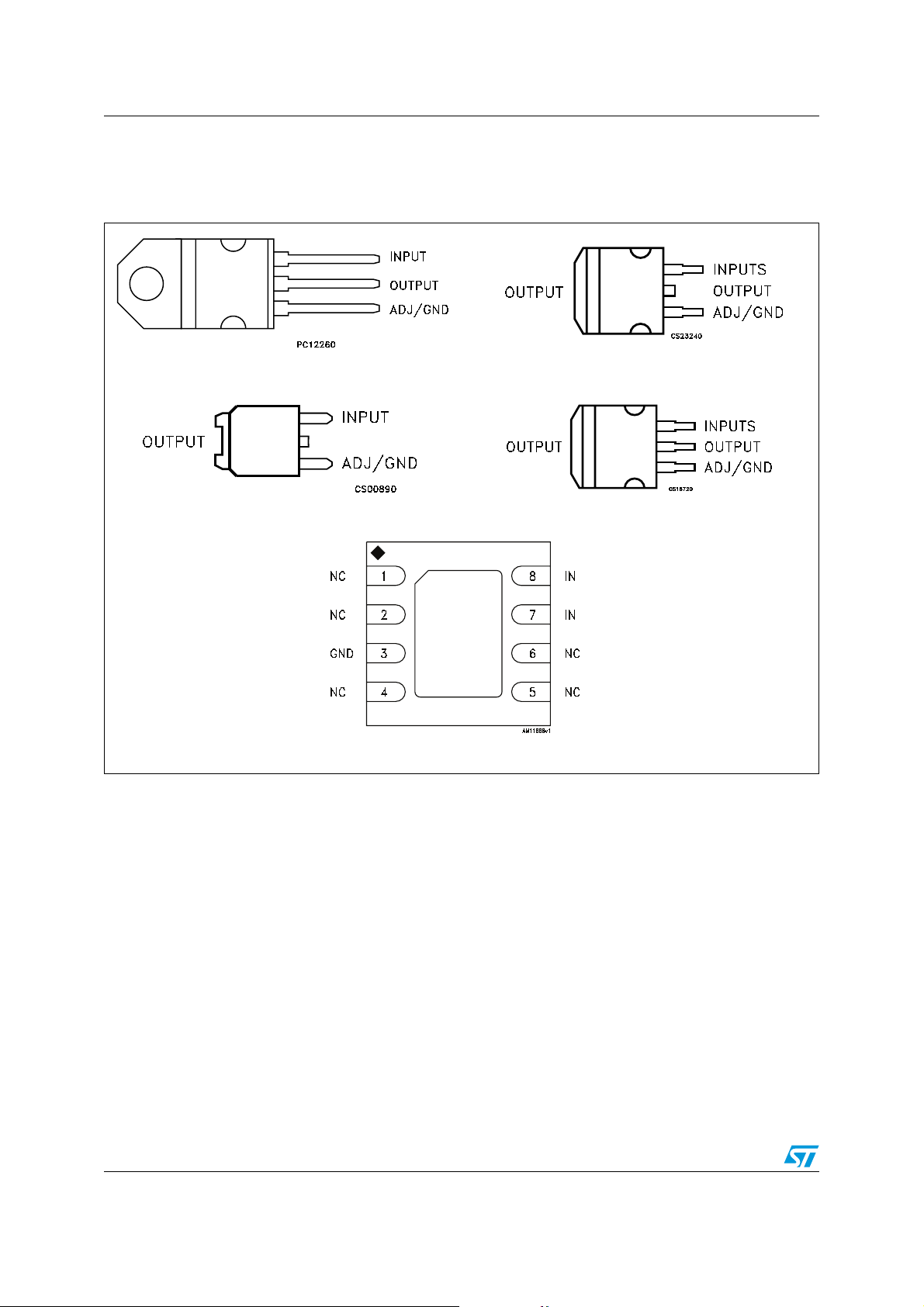
2 Pin configuration
Figure 2. Pin connections (top view)
TO-220
DPAK
OUTPUT
DFN8 (4X4)
D²PAK
D²PAK/A
Note: The TAB is physically connected to the output (this is valid for the TO-220 package too).
6/44 Doc ID 6739 Rev 27
LD1086xx Maximum ratings
3 Maximum ratings
Table 2. Absolute maximum ratings
Symbol Parameter Value Unit
DC input voltage 30 V
Output current Internally Limited mA
Power dissipation Internally Limited mW
Storage temperature range -55 to +150 °C
Operating junction temperature range -40 to +125 °C
T
P
T
V
I
I
O
D
STG
OP
Note: Absolute maximum ratings are those values beyond which damage to the device may occur.
Functional operation under these condition is not implied.
Table 3. Thermal data
Symbol Parameter TO-220
R
R
thJC
thJA
Thermal resistance junction-case 5 3 8 1.5 °C/W
Thermal resistance junction-ambient 50 62.5 33 °C/W
D²PAK
D²PAK/A
DPAK DFN8 Unit
Doc ID 6739 Rev 27 7/44
Schematic application LD1086xx
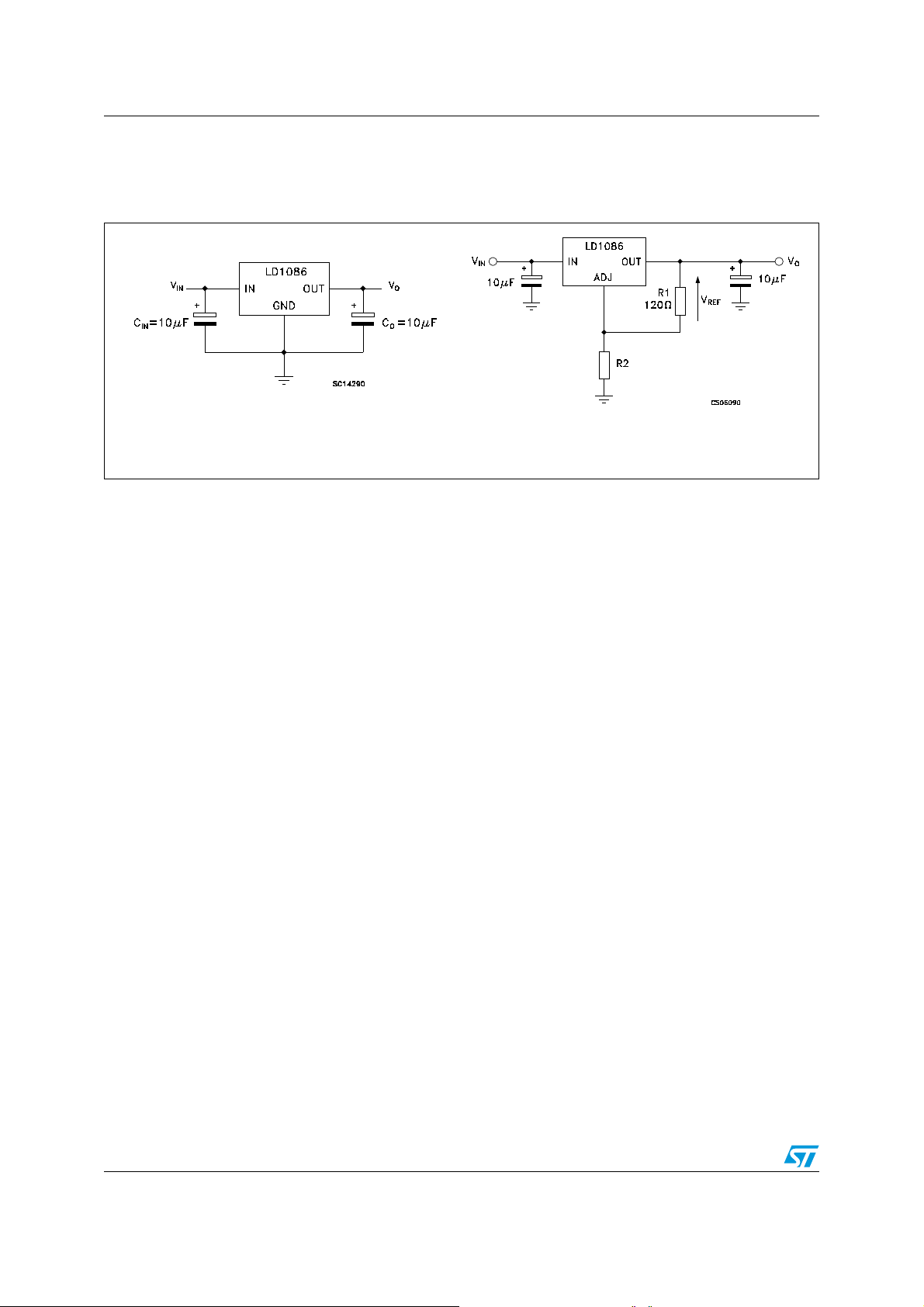
4 Schematic application
Figure 3. Application circuit
R
2
VOV
⎛⎞
1
⋅=
REF
⎝⎠
------ -+
R
1
8/44 Doc ID 6739 Rev 27
LD1086xx Electrical characteristics
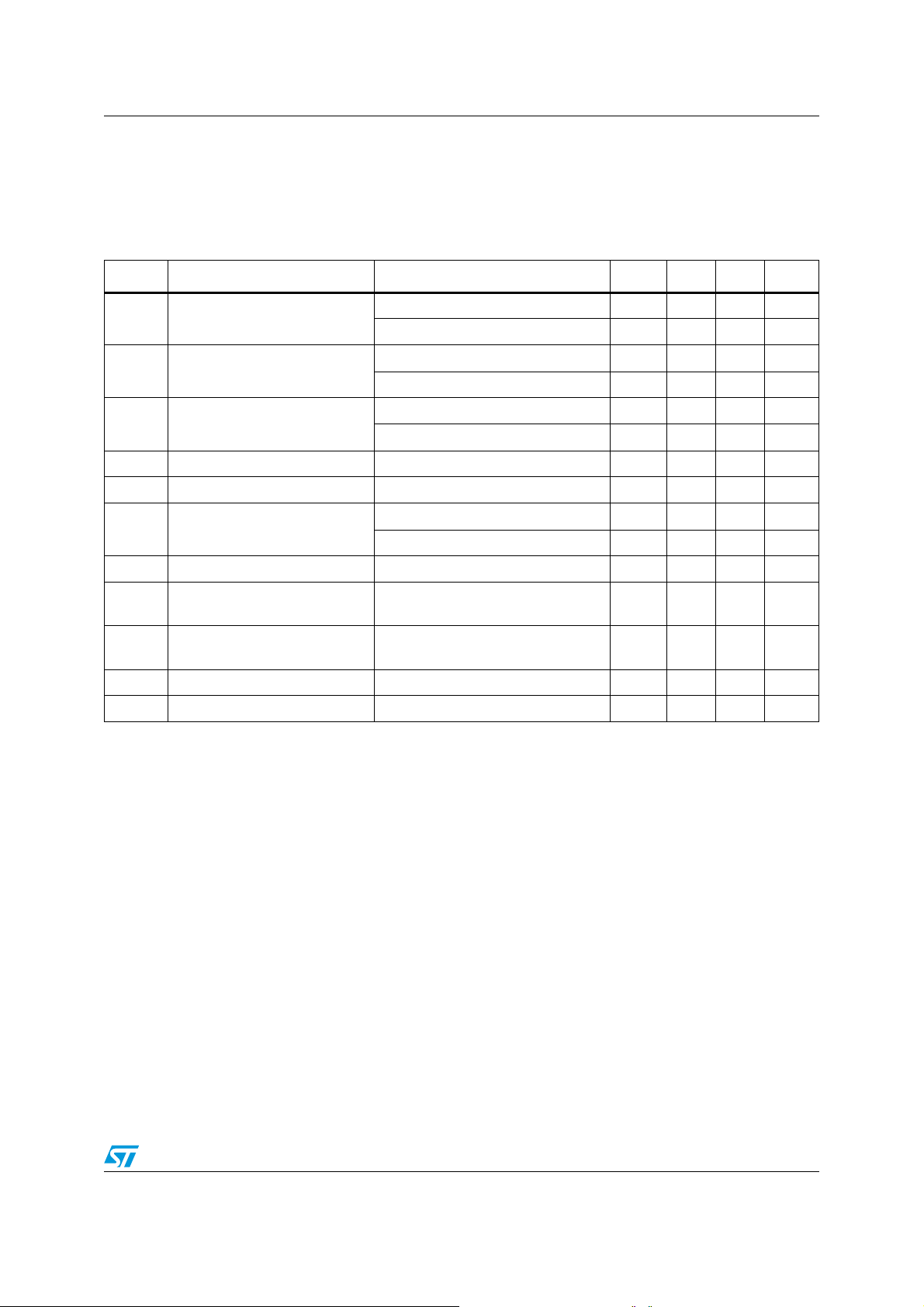
5 Electrical characteristics
VI = 4.8 V, CI = CO =10 µF, TA = -40 to 125 °C, unless otherwise specified.
Table 4. Electrical characteristics of LD1086#18
Symbol Parameter Test condition Min. Typ. Max. Unit
V
ΔV
ΔV
Output voltage
O
Line regulation
O
Load regulation
O
V
Dropout voltage IO = 1.5A 1.3 1.5 V
d
I
Quiescent current VI ≤ 30V 5 10 mA
q
I
Short circuit current
sc
(1)
Thermal regulation T
SVR Supply voltage rejection
RMS Output noise voltage (% of
eN
)
V
O
IO = 0 mA, TJ = 25°C 1.782 1.8 1.818 V
I
= 0 to 1.5A, VI = 3.4 to 30V 1.764 1.8 1.836 V
O
= 0 mA, VI = 3.4 to 18V, TJ = 25°C 0.2 4 mV
I
O
IO = 0 mA, VI = 3.4 to 15V 0.4 4 mV
I
= 0 to 1.5A, TJ = 25°C 0.5 8 mV
O
I
= 0 to 1.5A 1 16 mV
O
V
- VO = 5V 1.5 2 A
I
VI - VO = 25V 0.05 0.02 A
= 25°C, 30ms pulse 0.01 0.04 %/W
A
f = 120 Hz, C
V
= 6.8 ± 3V
I
= 25°C, f =10Hz to 10kHz 0.003 %
T
A
= 25 µF, IO = 1.5A
O
60 82 dB
S Temperature stability 0.5 %
S Long term stability T
1. See short-circuit current curve for available output current at fixed dropout.
= 125°C, 1000Hrs 0.5 %
A
Doc ID 6739 Rev 27 9/44

Electrical characteristics LD1086xx
VI = 5.5 V, CI = CO =10 µF, TA = -40 to 125 °C, unless otherwise specified.
Table 5. Electrical characteristics of LD1086#25
Symbol Parameter Test condition Min. Typ. Max. Unit
V
ΔV
ΔV
Output voltage
O
Line regulation
O
Load regulation
O
V
Dropout voltage IO = 1.5A 1.3 1.5 V
d
I
Quiescent current VI ≤ 30V 5 10 mA
q
Short circuit current
I
sc
(1)
Thermal regulation T
SVR Supply voltage rejection
RMS Output noise voltage (% of
eN
)
V
O
IO = 0 mA, TJ = 25°C 2.475 2.5 2.525 V
I
= 0 to 1.5A, VI = 4.1 to 30V 2.45 2.5 2.55 V
O
I
= 0 mA, VI = 4.1 to 18V, TJ = 25°C 0.2 4 mV
O
I
= 0 mA, VI = 4.1 to 18V 0.4 4 mV
O
= 0 to 1.5A, TJ = 25°C 0.5 8 mV
I
O
IO = 0 to 1.5A 1 16 mV
V
- VO = 5V 1.5 2 A
I
V
- VO = 25V 0.05 0.2 A
I
= 25°C, 30ms pulse 0.008 0.04 %/W
A
f = 120 Hz, CO = 25 µF, IO = 1.5A
= 7.5 ± 3V
V
I
60 81 dB
TA = 25°C, f =10Hz to 10kHz 0.003 %
S Temperature stability 0.5 %
S Long term stability T
1. See short-circuit current curve for available output current at fixed dropout.
= 125°C, 1000Hrs 0.5 %
A
10/44 Doc ID 6739 Rev 27

LD1086xx Electrical characteristics
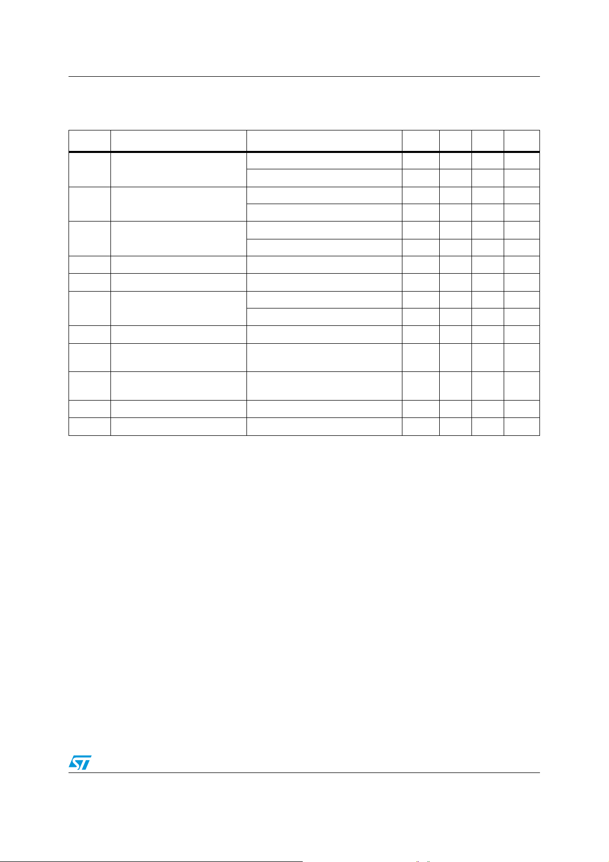
VI = 6.3 V, CI = CO =10 µF, TA = -40 to 125 °C, unless otherwise specified.
Table 6. Electrical characteristics of LD1086#33
Symbol Parameter Test condition Min. Typ. Max. Unit
V
ΔV
ΔV
Output voltage
O
Line regulation
O
Load regulation
O
V
Dropout voltage IO = 1.5A 1.3 1.5 V
d
I
Quiescent current VI ≤ 30V 5 10 mA
q
Short circuit current
I
sc
(1)
Thermal regulation T
SVR Supply voltage rejection
RMS Output noise voltage (% of
eN
)
V
O
IO = 0 mA, TJ = 25°C 3.267 3.3 3.333 V
I
= 0 to 1.5A, VI = 4.9 to 30V 3.234 3.3 3.366 V
O
I
= 0 mA, VI = 4.9 to 18V, TJ = 25°C 0.5 6 mV
O
I
= 0 mA, VI = 4.9 to 18V 1 6 mV
O
= 0 to 1.5A, TJ = 25°C 1 10 mV
I
O
IO = 0 to 1.5A 7 25 mV
V
- VO = 5V 1.5 2 A
I
V
- VO = 25V 0.05 0.2 A
I
= 25°C, 30ms pulse 0.008 0.04 %/W
A
f = 120 Hz, CO = 25 µF, IO = 1.5A
= 8.3 ± 3V
V
I
60 79 dB
TA = 25°C, f =10Hz to 10kHz 0.003 %
S Temperature stability 0.5 %
S Long term stability T
1. See short-circuit current curve for available output current at fixed dropout.
= 125°C, 1000Hrs 0.5 %
A
Doc ID 6739 Rev 27 11/44
Electrical characteristics LD1086xx
VI = 6.6 V, CI = CO =10 µF, TA = -40 to 125 °C, unless otherwise specified.
Table 7. Electrical characteristics of LD1086#36
Symbol Parameter Test condition Min. Typ. Max. Unit
V
ΔV
ΔV
Output voltage
O
Line regulation
O
Load regulation
O
V
Dropout voltage IO = 1.5A 1.3 1.5 V
d
I
Quiescent current VI ≤ 30V 5 10 mA
q
Short circuit current
I
sc
(1)
Thermal regulation T
SVR Supply voltage rejection
RMS Output noise voltage (% of
eN
)
V
O
IO = 0 mA, TJ = 25°C 3.564 3.6 3.636 V
I
= 0 to 1.5A, VI = 5.2 to 30V 3.528 3.6 3.672 V
O
I
= 0 mA, VI = 5.2 to 18V, TJ = 25°C 0.5 10 mV
O
I
= 0 mA, VI = 5.2 to 18V 1 10 mV
O
= 0 to 1.5A, TJ = 25°C 3 15 mV
I
O
IO = 0 to 1.5A 7 25 mV
V
- VO = 5V 1.5 2 A
I
V
- VO = 25V 0.05 0.2 A
I
= 25°C, 30ms pulse 0.01 0.04 %/W
A
f = 120 Hz, CO = 25 µF, IO = 1.5A
= 8.6 ± 3V
V
I
60 78 dB
TA = 25°C, f =10Hz to 10kHz 0.003 %
S Temperature stability 0.5 %
S Long term stability T
1. See short-circuit current curve for available output current at fixed dropout.
= 125°C, 1000Hrs 0.5 %
A
12/44 Doc ID 6739 Rev 27
LD1086xx Electrical characteristics
VI = 8 V, CI = CO =10 µF, TA = -40 to 125 °C, unless otherwise specified.
Table 8. Electrical characteristics of LD1086#50
Symbol Parameter Test condition Min. Typ. Max. Unit
V
ΔV
ΔV
Output voltage
O
Line regulation
O
Load regulation
O
V
Dropout voltage IO = 1.5A 1.3 1.5 V
d
I
Quiescent current VI ≤ 30V 5 10 mA
q
Short circuit current
I
sc
(1)
Thermal regulation T
SVR Supply voltage rejection
RMS Output noise voltage (% of
eN
)
V
O
IO = 0 mA, TJ = 25°C 4.95 5 5.05 V
I
= 0 to 1.5A, VI = 6.6 to 30V 4.9 5 5.1 V
O
I
= 0 mA, VI = 6.6 to 20V, TJ = 25°C 0.5 10 mV
O
I
= 0 mA, VI = 6.6 to 20V 1 10 mV
O
= 0 to 1.5A, TJ = 25°C 5 20 mV
I
O
IO = 0 to 1.5A 10 35 mV
V
- VO = 5V 1.5 2 A
I
V
- VO = 25V 0.05 0.2 A
I
= 25°C, 30ms pulse 0.01 0.04 %/W
A
f = 120 Hz, CO = 25 µF, IO = 1.5A
= 10 ± 3V
V
I
60 75 dB
TA = 25°C, f =10Hz to 10kHz 0.003 %
S Temperature stability 0.5 %
S Long term stability T
1. See short-circuit current curve for available output current at fixed dropout.
= 125°C, 1000Hrs 0.5 %
A
Doc ID 6739 Rev 27 13/44

Electrical characteristics LD1086xx
VI = 15 V, CI = CO =10 µF, TA = -40 to 125 °C, unless otherwise specified.
Table 9. Electrical characteristics of LD1086#12
Symbol Parameter Test condition Min. Typ. Max. Unit
V
ΔV
ΔV
Output voltage
O
Line regulation
O
Load regulation
O
V
Dropout voltage IO = 1.5A 1.3 1.5 V
d
I
Quiescent current VI ≤ 30V 5 10 mA
q
I
Short circuit current
sc
(1)
IO = 0 mA, TJ = 25°C 11.88 12 12.12 V
I
= 0 to 1.5A, VI = 13.8 to 30V 11.76 12 12.24 V
O
IO = 0 mA, VI = 13.8 to 25V,
= 25°C
T
J
= 0 mA, VI = 13.8 to 25V 2 25 mV
I
O
I
= 0 to 1.5A, TJ = 25°C 12 36 mV
O
I
= 0 to 1.5A 24 72 mV
O
V
- VO = 5V 1.5 2 A
I
V
- VO = 25V 0.05 0.2 A
I
125mV
Thermal regulation TA = 25°C, 30ms pulse 0.01 0.04 %/W
SVR Supply voltage rejection
RMS Output noise voltage (% of
eN
)
V
O
f = 120 Hz, C
= 17 ± 3V
V
I
= 25°C, f =10Hz to 10kHz 0.003 %
T
A
= 25 µF, IO = 1.5A
O
54 66 dB
S Temperature stability 0.5 %
S Long term stability T
1. See short-circuit current curve for available output current at fixed dropout.
= 125°C, 1000Hrs 0.5 %
A
14/44 Doc ID 6739 Rev 27

LD1086xx Electrical characteristics
VI = 4.25 V, CI = CO =10 µF, TA = -40 to 125 °C, unless otherwise specified.
Table 10. Electrical characteristics of LD1086#
Symbol Parameter Test condition Min. Typ. Max. Unit
V
ΔV
ΔV
V
I
O(min)
I
sc
Output voltage
O
Line Regulation
O
Load Regulation
O
Dropout Voltage IO = 1.5A 1.3 1.5 V
d
(1)
Minimum Load Current VI = 30V 3 10 mA
Short Circuit Current
IO = 10mA TJ = 25°C 1.237 1.25 1.263 V
I
= 10mA to 1.5A, VI = 2.85 to 30V 1.225 1.25 1.275 V
O
IO = 10mA, VI = 2.8 to 16.5V,
= 25°C
T
J
= 10mA, VI = 2.8 to 16.5V 0.035 0.2 %
I
O
I
= 10mA to 1.5A, TJ = 25°C 0.1 0.3 %
O
I
= 0 to 1.5A 0.2 0.4 %
O
V
- VO = 5V 1.5 2.3 A
I
V
- VO = 25V 0.05 0.2 A
I
0.015 0.2 %
Thermal Regulation TA = 25°C, 30ms pulse 0.01 0.04 %/W
SVR Supply Voltage Rejection
I
ΔI
Adjust Pin Current VI = 4.25V, IO = 10 mA 40 120 µA
ADJ
Adjust Pin Current Change
ADJ
RMS Output Noise Voltage (%
eN
of V
)
O
f = 120 Hz, C
= 1.5A, VI = 6.25 ± 3V
I
O
(1)
IO = 10mA to 1.5A, VI = 2.8 to 16.5V 0.2 5 µA
= 25 µF,C
O
TA = 25°C, f =10Hz to 10kHz 0.003 %
ADJ
= 25 µF,
60 88 dB
S Temperature Stability 0.5 %
S Long Term Stability T
1. See short-circuit current curve for available output current at fixed dropout.
= 125°C, 1000Hrs 0.5 %
A
Doc ID 6739 Rev 27 15/44

Electrical characteristics LD1086xx
VI = 4.25 V, CI = CO =10 µF, TA = -40 to 125 °C, unless otherwise specified.
Table 11. Electrical characteristics of LD1086DTTRY and LD1086VY (Automotive Grade)
Symbol Parameter Test condition Min. Typ. Max. Unit
V
ΔV
ΔV
V
I
O(min)
I
sc
Output voltage
O
Line regulation IO = 10 mA, VI = 2.8 to 16.5 V 0.035 0.2 %
O
Load regulation IO = 0 to 1.5 A 0.2 0.4 %
O
Dropout voltage IO = 1.5 A 1.3 1.5 V
d
(1)
Minimum load current VI = 30 V 3 10 mA
Short circuit current
IO = 10 mA TA = 25°C 1.237 1.25 1.263 V
I
= 10 mA to 1.5 A, VI = 2.85 to 30 V 1.225 1.25 1.275 V
O
V
- VO = 5 V, TA = 25°C 1.5 2.3 A
I
V
- VO = 25 V, TA = 25°C 0.05 0.2 A
I
Thermal regulation TA = 25°C, 30ms pulse 0.01 0.04 %/W
SVR Supply voltage rejection
I
ΔI
Adjust pin current VI = 4.25 V, IO = 10 mA 40 120 μA
ADJ
Adjust pin current change
ADJ
RMS output noise voltage (%
eN
of V
)
O
f = 120 Hz, C
= 1.5 A, VI = 6.25 ± 3 V, TA = 25°C
I
O
(1)
IO = 10 mA to 1.5 A, VI = 2.8 to 16.5 V 0.2 5 μA
= 25 µF,C
O
TA = 25°C, f =10 Hz to 10 kHz 0.003 %
ADJ
= 25 µF,
60 88 dB
S Temperature stability 0.5 %
S Long term stability T
1. See short-circuit current curve for available output current at fixed dropout.
= 125°C, 1000 Hrs 0.5 %
A
16/44 Doc ID 6739 Rev 27

LD1086xx Typical application
6 Typical application
Unless otherwise specified TJ = 25 °C, CI = CO = 10 µF.
Figure 4. Output voltage vs. temp. (VI = 5 V) Figure 5. Output voltage vs. temp. (VI = 15 V)
Figure 6. Output voltage vs. temperature
(V
= 4.25 V)
Figure 8. Line regulation vs. temperature Figure 9. Load regulation vs. temperature
I
Figure 7. Short circuit current vs. dropout
voltage
Doc ID 6739 Rev 27 17/44

Typical application LD1086xx
Figure 10. Dropout voltage vs. temperature Figure 11. Dropout voltage vs. output current
Figure 12. Adjust pin current vs. input voltage Figure 13. Adjust pin current vs. temperature
Figure 14. Adjust pin current vs. output
current
Figure 15. Quiescent current vs. output
18/44 Doc ID 6739 Rev 27
current

LD1086xx Typical application
Figure 16. Quiescent current vs. input voltage Figure 17. Supply voltage rejection vs. output
current
Figure 18. Supply voltage rejection vs.
frequency
Figure 20. Minimum load current vs.
temperature
Figure 19. Supply voltage rejection vs.
temperature
Figure 21. Stability for adjustable
Doc ID 6739 Rev 27 19/44

Typical application LD1086xx
Figure 22. Stability for 2.85 V Figure 23. Stability for 12 V
Figure 24. Line transient (VI = 12 to 13 V) Figure 25. Line transient (IO = 200 mA)
VI = 12 to 13 V, IO = 200 mA, CI = 1 µF (tant), CO = 10 µF
(tant), No C
Figure 26. Line transient (C
ADJ
= 1 µF) Figure 27. Load transient
ADJ
VI = 12 to 13 V, IO = 200 mA, CI = 1 µF (tant), CO = 10 µF
ADJ
= 1 µF
(tant), C
VI = 12 to 13 V, IO = 200 mA, CI = 1 µF (tant), CO = 10 µF
(tant), No C
VI = 13 V, IO = 0.1 to 1.5 A, CI = 1 µF (tant), CO = 10 µF
(tant) C
20/44 Doc ID 6739 Rev 27
ADJ
ADJ
= 1 µF

LD1086xx Typical application
Figure 28. Load transient (T
rise
= T
= 10 µs) Figure 29. Thermal protection
fall
VI = 13 V, IO = 0.1 to 1.5 A, CI = 1 µF (tant), CO = 10 µF
ADJ
= 1 µF
(tant), C
VO = 2.85 V
Doc ID 6739 Rev 27 21/44

Package mechanical data LD1086xx
7 Package mechanical data
In order to meet environmental requirements, ST offers these devices in different grades of
®
ECOPACK
specifications, grade definitions and product status are available at:
ECOPACK
packages, depending on their level of environmental compliance. ECOPACK®
®
is an ST trademark.
www.st.com
Table 12. TO-220 mechanical data
Type STD - ST Dual Gauge Type STD - ST Single Gauge
Dim.
Min. Typ. Max. Min. Typ. Max.
A 4.40 4.60 4.40 4.60
b 0.61 0.88 0.61 0.88
b1 1.14 1.70 1.14 1.70
c 0.48 0.70 0.48 0.70
D 15.25 15.75 15.25 15.75
D1 1.27
E 10.00 10.40 10.00 10.40
e 2.40 2.70 2.40 2.70
mm. mm.
.
e1 4.95 5.15 4.95 5.15
F 1.23 1.32 0.51 0.60
H1 6.20 6.60 6.20 6.60
J1 2.40 2.72 2.40 2.72
L 13.00 14.00 13.00 14.00
L1 3.50 3.93 3.50 3.93
L20 16.40 16.40
L30 28.90 28.90
∅P 3.75 3.85 3.75 3.85
Q 2.65 2.95 2.65 2.95
In spite of some difference in tolerances, the packages are compatible.
22/44 Doc ID 6739 Rev 27

LD1086xx Package mechanical data
Figure 30. Drawing dimension TO-220 (type STD-ST Dual Gauge)
Note: 1 Maximum resin gate protrusion: 0.5 mm.
2 Resin gate position is accepted in each of the two positions shown on the drawing, or their
symmetrical.
Doc ID 6739 Rev 27 23/44
0015988_S

Package mechanical data LD1086xx
Figure 31. Drawing dimension TO-220 (type STD-ST Single Gauge)
24/44 Doc ID 6739 Rev 27
8174627_B

LD1086xx Package mechanical data
Figure 32. Drawing dimension tube for TO-220 Dual Gauge (mm.)
Figure 33. Drawing dimension tube for TO-220 Single Gauge (mm.)
Doc ID 6739 Rev 27 25/44

Package mechanical data LD1086xx
DPAK mechanical data
Dim.
mm. inch.
Min. Typ. Max. Min. Typ. Max.
A 2.2 2.4 0.086 0.094
A1 0.9 1.1 0.035 0.043
A2 0.03 0.23 0.001 0.009
B 0.64 0.9 0.025 0.035
b4 5.2 5.4 0.204 0.212
C 0.45 0.6 0.017 0.023
C2 0.48 0.6 0.019 0.023
D 6 6.2 0.236 0.244
D1 5.1 0.200
E 6.4 6.6 0.252 0.260
E1 4.7 0.185
e2.28 0.090
e1 4.4 4.6 0.173 0.181
H 9.35 10.1 0.368 0.397
L 1 0.039
(L1)
2.8 0.110
L2 0.8 0.031
L4 0.6 1 0.023 0.039
R 0.2 0.008
V2 0° 8°0° 8°
26/44 Doc ID 6739 Rev 27
0068772-F

LD1086xx Package mechanical data
Figure 34. Drawing dimension D²PAK (type STD-ST)
0079457/L
Doc ID 6739 Rev 27 27/44

Package mechanical data LD1086xx
Figure 35. Drawing dimension D²PAK (type WOOSEOK-SUBCON.)
28/44 Doc ID 6739 Rev 27
0079457/L

LD1086xx Package mechanical data
Table 13. D²PAK mechanical data
Type STD-ST Type WOOSEOK-Subcon.
Dim.
Min. Typ. Max. Min. Typ. Max.
A 4.40 4.60 4.30 4.70
A1 0.03 0.23 0 0.20
b 0.70 0.93 0.70 0.90
b2 1.14 1.70 1.17 1.37
c 0.45 0.60 0.45 0.50 0.60
c2 1.23 1.36 1.25 1.30 1.40
D 8.95 9.35 9 9.20 9.40
D1 7.50 7.50
E 10 10.40 9.80 10.20
E1 8.50 7.50
e2.54 2.54
e1 4.88 5.28 5.08
H 15 15.85 15 15.30 15.60
J1 2.49 2.69 2.20 2.60
L 2.29 2.79 1.79 2.79
mm. mm.
L1 1.27 1.40 1 1.40
L2 1.30 1.75 1.20 1.60
R0.4 0.30
V2 0° 8° 0° 3°
Note: The D²PAK package coming from the subcontractor Wooseok is fully compatible with the
ST's package suggested footprint.
Doc ID 6739 Rev 27 29/44

Package mechanical data LD1086xx
Figure 36. D²PAK footprint recommended data
Table 14. Footprint data
A 12.20 0.480
B 9.75 0.384
C 16.90 0.665
D 3.50 0.138
E 1.60 0.063
F 2.54 0.100
G 5.08 0.200
Val ues
mm. inch.
30/44 Doc ID 6739 Rev 27

LD1086xx Package mechanical data
Figure 37. Drawing dimension D²PAK/A (type STD-ST)
7106164/E
Doc ID 6739 Rev 27 31/44

Package mechanical data LD1086xx
Figure 38. Drawing dimension D²PAK/A (type WOOSEOK-Subcon.)
32/44 Doc ID 6739 Rev 27
7106164/E

LD1086xx Package mechanical data
Table 15. D²PAK/A mechanical data
Type STD-ST Type WOOSEOK-Subcon.
Dim.
Min. Typ. Max. Min. Typ. Max.
A 4.40 4.60 4.30 4.70
A1 0.03 0.23 0 0.20
b 0.70 0.93 0.70 0.90
b1 0.80 1.30
b2 1.14 1.70 1.17 1.37
c 0.45 0.60 0.45 0.50 0.60
c2 1.23 1.36 1.25 1.30 1.40
D 8.95 9.35 9 9.20 9.40
D1 7.50 7.50
E 10 10.40 9.80 10.20
E1 8.50 7.50
e2.54 2.54
e1 4.88 5.28 5.08
H 15 15.85 15 15.30 15.60
J1 2.49 2.69 2.20 2.60
mm. mm.
L 2.29 2.79 1.79 2.79
L1 1.27 1.40 1 1.40
R0.4 0.30
V2 0° 8° 0° 3°
Note: The D²PAK/A package coming from the subcontractor Wooseok is fully compatible with the
ST's package suggested footprint.
Doc ID 6739 Rev 27 33/44

Package mechanical data LD1086xx
Figure 39. D²PAK/A footprint recommended data
Table 16. Footprint data
A 12.20 0.480
B 9.75 0.384
C 16.90 0.665
D 3.50 0.138
E 1.60 0.063
F 2.54 0.100
G 5.08 0.200
Val ues
mm. inch.
34/44 Doc ID 6739 Rev 27

LD1086xx Package mechanical data
Table 17. DFN8L (4x4 mm.) mechanical data
Dim.
Min. Typ. Max.
A 0.80 0.90 1
A1 0 0.02 0.05
A3 0,20
b 0.23 0.30 0.38
D 3.90 4 4.10
D2 2.82 3 3.23
E 3.90 4 4.10
E2 2.05 2.20 2.30
e0.80
L 0.40 0.50 0.60
mm.
Doc ID 6739 Rev 27 35/44

Package mechanical data LD1086xx
Figure 40. DFN8L package outline
36/44 Doc ID 6739 Rev 27

LD1086xx Package mechanical data
Figure 41. DFN8L footprint - recommended data
Doc ID 6739 Rev 27 37/44

Package mechanical data LD1086xx
Figure 42. DFN8L carrier tape (dimension are in mm.)
38/44 Doc ID 6739 Rev 27
7279936

LD1086xx Package mechanical data
Figure 43. Reel DFN8L drawing
Table 18. Reel DFN8L dimensions
Dim.
Min. Typ. Max. Min. Typ. Max.
A 330 12.992
C 12.8 13.0 13.2 0.504 0.512 0.519
D20.2 0.795
N60 2.362
T 22.4 0.882
mm. inch.
Doc ID 6739 Rev 27 39/44

Package mechanical data LD1086xx
Tape & reel DPAK-PPAK mechanical data
Dim.
Min. Typ. Max. Min. Typ. Max.
A 330 12.992
C12.8 13.0 13.2 0.504 0.512 0.519
D 20.2 0.795
N60 2.362
T22.40.882
Ao 6.806.90 7.00 0.268 0.272 0.2.76
Bo 10.40 10.50 10.60 0.409 0.413 0.417
Ko 2.55 2.65 2.75 0.100 0.104 0.105
Po 3.9 4.0 4.1 0.153 0.157 0.161
P7.98.0 8.1 0.311 0.315 0.319
mm. inch.
40/44 Doc ID 6739 Rev 27

LD1086xx Package mechanical data
Tape & reel D2PAK-P2PAK-D2PAK/A-P2PAK/A mechanical data
Dim.
Min. Typ. Max. Min. Typ. Max.
A180 7.086
C 12.8 13.0 13.2 0.504 0.512 0.519
D 20.2 0.795
N60 2.362
T 14.4 0.567
Ao 10.50 10.6 10.70 0.413 0.417 0.421
Bo 15.70 15.80 15.90 0.618 0.622 0.626
Ko 4.804.90 5.00 0.189 0.193 0.197
Po 3.9 4.0 4.1 0.153 0.157 0.161
P 11.9 12.0 12.1 0.468 0.472 0.476
mm. inch.
Doc ID 6739 Rev 27 41/44

Order codes LD1086xx
8 Order codes
Table 19. Order codes
Packages
TO-220 D²PAK D²PAK/A DPAK DFN8
LD1086V18 LD1086D2T18TR LD1086DT18TR 1.8 V
LD1086D2T25TR LD1086DT25TR 2.5 V
LD1086V33 LD1086D2T33TR LD1086D2M33TR LD1086DT33TR 3.3 V
LD1086D2T50TR LD1086DT50TR 5.0 V
LD1086D2T12TR 12.0 V
LD1086V LD1086D2TTR LD1086D2MTR LD1086DTTR LD1086PUR ADJ
(2)
(1)
LD1086DTTRY
(2)
LD1086V-DG
LD1086VY
1. TO-220 Dual Gauge frame.
2. Automotive Grade products.
Output
voltages
ADJ
ADJ
42/44 Doc ID 6739 Rev 27

LD1086xx Revision history
9 Revision history
Table 20. Document revision history
Date Revision Changes
16-May-2006 14 Order codes updated and new template.
19-Jan-2007 15 D²PAK mechanical data updated and add footprint data.
05-Apr-2007 16 Order codes updated.
07-Jun-2007 17 Order codes updated.
19-Jul-2007 18 Add note on
03-Dec-2007 19 Modified:
31-Jan-2008 20 Added new order codes for Automotive grade products.
18-Feb-2008 21 Modified:
14-Jul-2008 22 Modified:
10-Mar-2010 23
15-Nov-2010 24 Modified: R
11-Jul-2011 25 Modified:
10-Feb-2012 26 Added: order code LD1086V-DG
15-Mar-2012 27
Added:
Figure 32
Added: new order code LD1086PUR
mechanical data DFN8 (4x4 mm)
Figure 41 on page 37, Figure 42 on page 38
Figure 2
Ta b l e 1 9
Table 19 on page 42
Table 1 on page 1
.
.
.
and
Table 19 on page 42
Table 12 on page 22, Figure 30 on page 23, Figure 31 on page 24
and
Figure 33 on page 25
value for TO-220
thJC
Figure 24, Figure 25 on page 20
.
Table 3 on page 7
and
Table 19 on page 42
.
Table 19 on page 42
Table 19 on page 42
Table 17 on page 35, Figure 40 on page 36
and
Figure 43 on page 39
.
,
.
.
and new package
,
.
Doc ID 6739 Rev 27 43/44

LD1086xx
Please Read Carefully:
Information in this document is provided solely in connection with ST products. STMicroelectronics NV and its subsidiaries (“ST”) reserve the
right to make changes, corrections, modifications or improvements, to this document, and the products and services described herein at any
time, without notice.
All ST products are sold pursuant to ST’s terms and conditions of sale.
Purchasers are solely responsible for the choice, selection and use of the ST products and services described herein, and ST assumes no
liability whatsoever relating to the choice, selection or use of the ST products and services described herein.
No license, express or implied, by estoppel or otherwise, to any intellectual property rights is granted under this document. If any part of this
document refers to any third party products or services it shall not be deemed a license grant by ST for the use of such third party products
or services, or any intellectual property contained therein or considered as a warranty covering the use in any manner whatsoever of such
third party products or services or any intellectual property contained therein.
UNLESS OTHERWISE SET FORTH IN ST’S TERMS AND CONDITIONS OF SALE ST DISCLAIMS ANY EXPRESS OR IMPLIED
WARRANTY WITH RESPECT TO THE USE AND/OR SALE OF ST PRODUCTS INCLUDING WITHOUT LIMITATION IMPLIED
WARRANTIES OF MERCHANTABILITY, FITNESS FOR A PARTICULAR PURPOSE (AND THEIR EQUIVALENTS UNDER THE LAWS
OF ANY JURISDICTION), OR INFRINGEMENT OF ANY PATENT, COPYRIGHT OR OTHER INTELLECTUAL PROPERTY RIGHT.
UNLESS EXPRESSLY APPROVED IN WRITING BY TWO AUTHORIZED ST REPRESENTATIVES, ST PRODUCTS ARE NOT
RECOMMENDED, AUTHORIZED OR WARRANTED FOR USE IN MILITARY, AIR CRAFT, SPACE, LIFE SAVING, OR LIFE SUSTAINING
APPLICATIONS, NOR IN PRODUCTS OR SYSTEMS WHERE FAILURE OR MALFUNCTION MAY RESULT IN PERSONAL INJURY,
DEATH, OR SEVERE PROPERTY OR ENVIRONMENTAL DAMAGE. ST PRODUCTS WHICH ARE NOT SPECIFIED AS "AUTOMOTIVE
GRADE" MAY ONLY BE USED IN AUTOMOTIVE APPLICATIONS AT USER’S OWN RISK.
Resale of ST products with provisions different from the statements and/or technical features set forth in this document shall immediately void
any warranty granted by ST for the ST product or service described herein and shall not create or extend in any manner whatsoever, any
liability of ST.
ST and the ST logo are trademarks or registered trademarks of ST in various countries.
Information in this document supersedes and replaces all information previously supplied.
The ST logo is a registered trademark of STMicroelectronics. All other names are the property of their respective owners.
© 2012 STMicroelectronics - All rights reserved
STMicroelectronics group of companies
Australia - Belgium - Brazil - Canada - China - Czech Republic - Finland - France - Germany - Hong Kong - India - Israel - Italy - Japan -
Malaysia - Malta - Morocco - Philippines - Singapore - Spain - Sweden - Switzerland - United Kingdom - United States of America
www.st.com
44/44 Doc ID 6739 Rev 27
 Loading...