

3 A low drop positive voltage regulator adjustable and fixed
Features
■ Typical dropout 1.3 V (at 3 A)
■ Three terminal adjustable or fixed output
voltage 1.5 V, 1.8 V, 2.5 V, 3.3 V, 5 V, 12 V.
■ Automotive grade product: adjustable V
only in TO-220 full pack package
■ Guaranteed output current up to 3 A
■ Output tolerance ± 1 % at 25°C and ± 2 % in full
temperature range
■ Internal power and thermal limit
■ Wide operating temperature range -40 °C to
125 °C
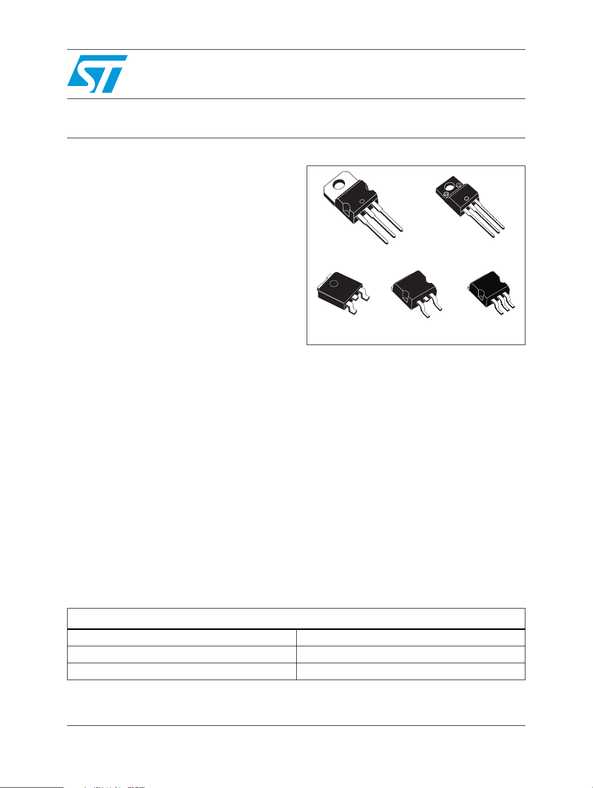
■ Package available: TO-220, TO-220FP,
2
DPAK, D
■ Pinout compatibility with standard adjustable
PAK, D2PAK/A
VREG
Description
The LD1085xx is a low drop voltage regulator
able to provide up to 3 A of output current.
Dropout is guaranteed at a maximum of 1.2 V at
the maximum output current, decreasing at lower
loads. The LD1085xx is pin to pin compatible with
the older 3-terminal adjustable regulators, but has
better performances in term of drop and output
tolerance.
A 2.85 V output version is suitable for SCSI-2
active termination. Unlike PNP regulators, where
a part of the output current is wasted as quiescent
current, the LD1085xx quiescent current flows
OUT
LD1085xx
TO-220
D2PAKDPAK
into the load, so increase efficiency. Only a 10 µF
minimum capacitor is need for stability.
The device is supplied in TO-220, TO-220FP,
DPAK, D
2
PAK and D2PAK/A. On chip trimming
allows the regulator to reach a very tight output
voltage tolerance, within ± 1 % at 25 °C.
The LD1085xx is available as automotive grade in
TO-220FP package only, for the option of
adjustable output voltage whose commercial part
number is shown in the Table 11: Order codes.
This device is qualified according to the
specification AEC-Q100 of the automotive
market, in the temperature range -40 °C to
125 °C, and the statistical tests PAT, SYL, SBL are
performed.
TO-220FP
D2PAK/A
Table 1. Device summary
Part numbers
July 2009 Doc ID 6738 Rev 25 1/28
LD1085XX LD1085XX25
LD1085XX15 LD1085XX33
LD1085XX18 LD1085XX50
www.st.com
28

Contents LD1085xx
Contents
1 Diagram . . . . . . . . . . . . . . . . . . . . . . . . . . . . . . . . . . . . . . . . . . . . . . . . . . . 3
2 Pin configuration . . . . . . . . . . . . . . . . . . . . . . . . . . . . . . . . . . . . . . . . . . . 4
3 Maximum ratings . . . . . . . . . . . . . . . . . . . . . . . . . . . . . . . . . . . . . . . . . . . . 5
4 Schematic application . . . . . . . . . . . . . . . . . . . . . . . . . . . . . . . . . . . . . . . 6
5 Electrical characteristics . . . . . . . . . . . . . . . . . . . . . . . . . . . . . . . . . . . . . 7
6 Typical application . . . . . . . . . . . . . . . . . . . . . . . . . . . . . . . . . . . . . . . . . 14
7 Package mechanical data . . . . . . . . . . . . . . . . . . . . . . . . . . . . . . . . . . . . 18
8 Order codes . . . . . . . . . . . . . . . . . . . . . . . . . . . . . . . . . . . . . . . . . . . . . . 26
9 Revision history . . . . . . . . . . . . . . . . . . . . . . . . . . . . . . . . . . . . . . . . . . . 27
2/28 Doc ID 6738 Rev 25
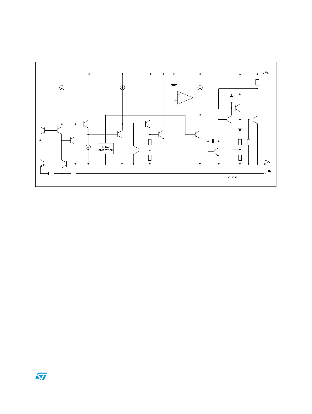
LD1085xx Diagram
1 Diagram
Figure 1. Schematic diagram
Doc ID 6738 Rev 25 3/28
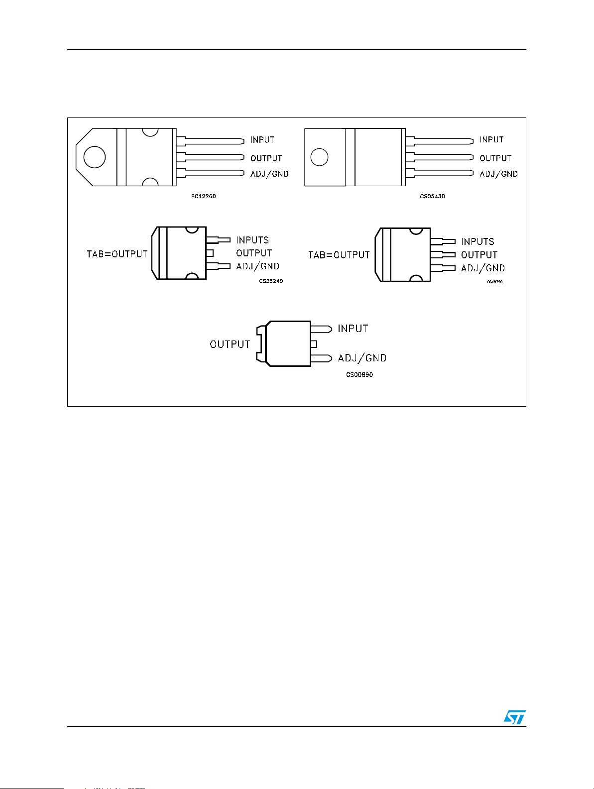
Pin configuration LD1085xx
2 Pin configuration
Figure 2. Pin connections (top view)
TO-220
D2PAK
TO-220FP
D2PAK/A
DPAK
4/28 Doc ID 6738 Rev 25
LD1085xx Maximum ratings
3 Maximum ratings
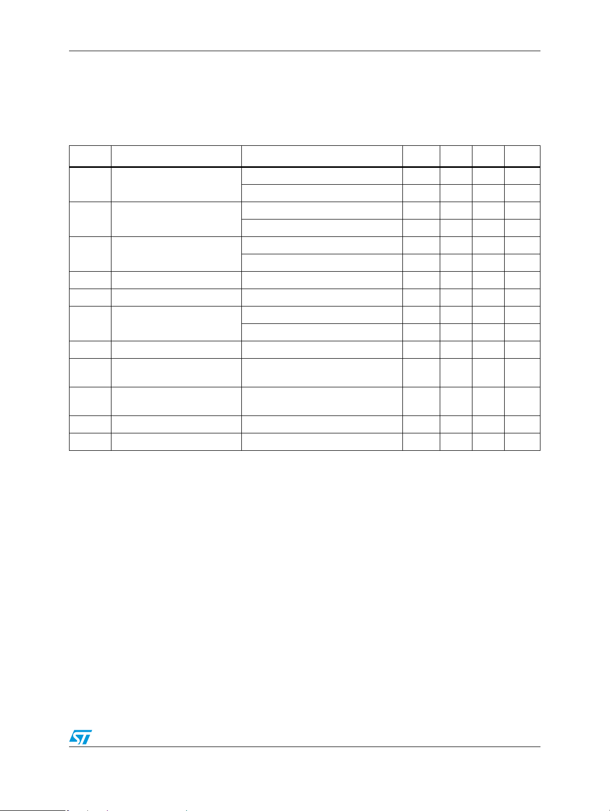
Table 2. Absolute maximum ratings
Symbol Parameter Value Unit
T
P
T
V
I
I
O
D
STG
OP
DC input voltage 30 V
Output current Internally limited mA
Power dissipation Internally limited mW
Storage temperature range -55 to +150 °C
Operating junction temperature range -40 to +125 °C
Note: Absolute maximum ratings are those values beyond which damage to the device may occur.
Functional operation under these condition is not implied
Table 3. Thermal data
2
PAK
Symbol Parameter TO-220 TO-220FP DPAK
R
R
thJC
thJA
Thermal resistance junction-case 3 5 8 3 °C/W
Thermal resistance junction-ambient 50 60 100 62.5 °C/W
D
D2PAK/A
Unit
Doc ID 6738 Rev 25 5/28
Schematic application LD1085xx
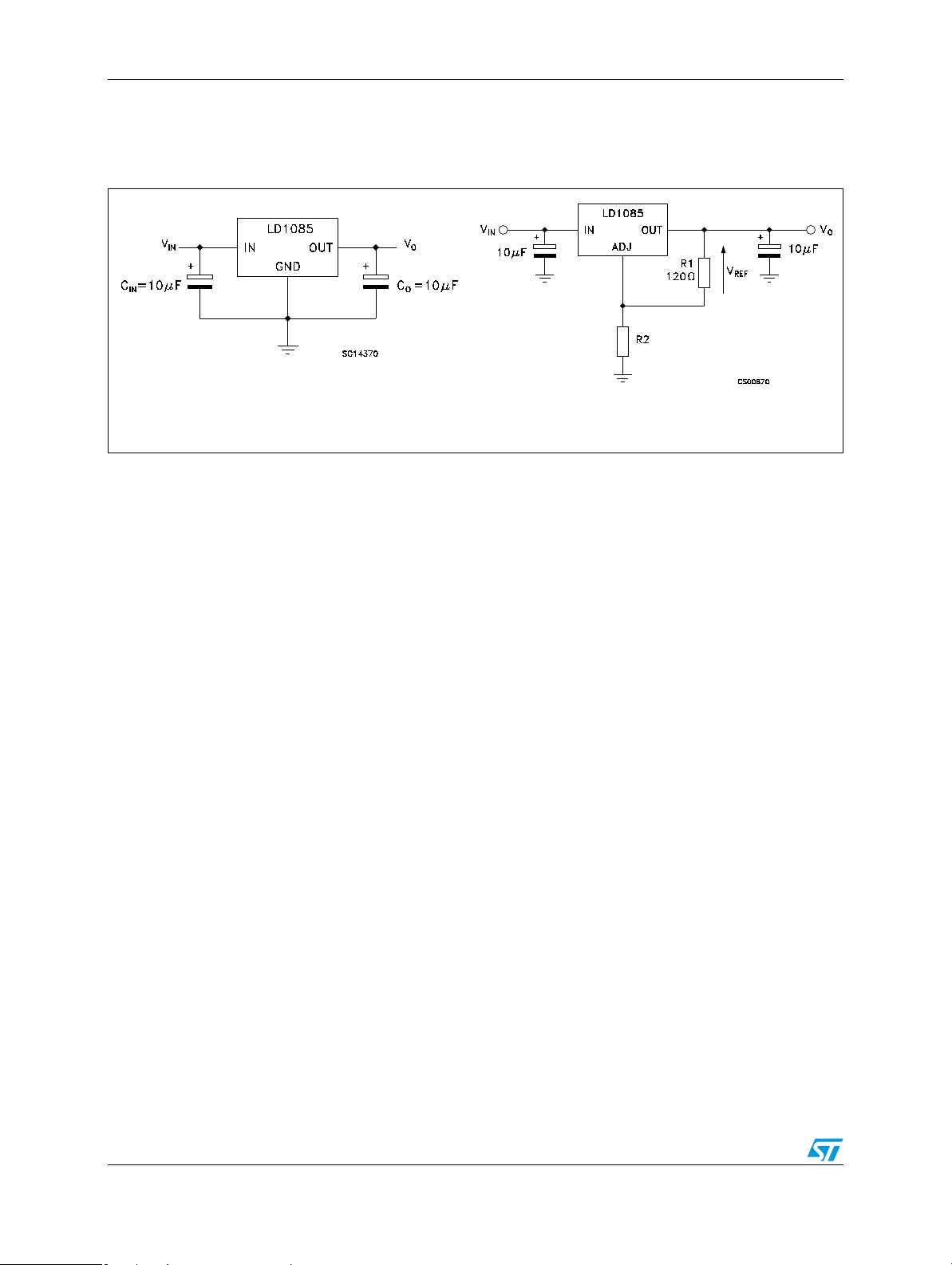
4 Schematic application
Figure 3. Application circuit
R
2
VOV
⎛⎞
1
⋅=
REF
⎝⎠
------ -+
R
1
6/28 Doc ID 6738 Rev 25
LD1085xx Electrical characteristics
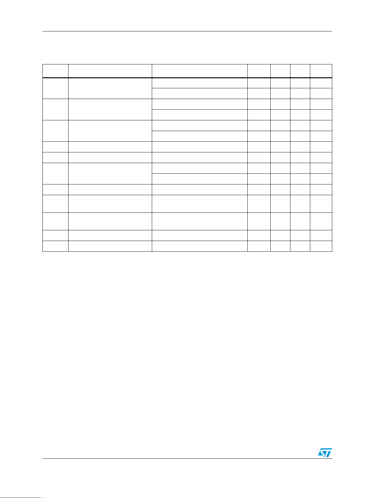
5 Electrical characteristics
VI = 4.5 V, CI = CO =10 µF, TA = -40 to 125 °C, unless otherwise specified.
Table 4. Electrical characteristics of LD1085#15
Symbol Parameter Test condition Min. Typ. Max. Unit
V
ΔV
ΔV
V
Output voltage
O
Line regulation
O
Load regulation
O
Dropout voltage IO =3 A 1.3 1.5 V
d
Quiescent current VI ≤ 30 V 5 10 mA
I
q
I
Short circuit current
sc
(1)
Thermal regulation T
SVR Supply voltage rejection
eN
RMS output noise voltage (%
)
of V
O
IO = 0 mA, TJ = 25°C 1.485 1.5 1.515 V
= 0 to 3 A, VI = 3.1 to 30 V 1.47 1.5 1.53 V
I
O
I
= 0 mA, VI = 3.1 to 18 V, TJ = 25°C 0.2 4 mV
O
I
= 0 mA, VI = 3.1 to 15 V 0.4 4 mV
O
I
= 0 to 3 A, TJ = 25°C 2 10 mV
O
= 0 to 3 A 4 20 mV
I
O
V
- VO = 5 V 3.2 4.5 A
I
V
- VO = 25 V 0.2 0.5 A
I
= 25°C, 30ms pulse 0.008 0.04 %/W
A
f = 120 Hz, C
= 7.5 ± 3 V
V
I
T
= 25°C, f =10 Hz to 10 kHz 0.003 %
A
= 25 µF, IO = 3 A
O
60 72 dB
S Temperature stability 0.5 %
S Long term stability T
1. See short-circuit current curve for available output current at fixed dropout.
= 125°C, 1000Hrs 0.5 %
A
Doc ID 6738 Rev 25 7/28
Electrical characteristics LD1085xx
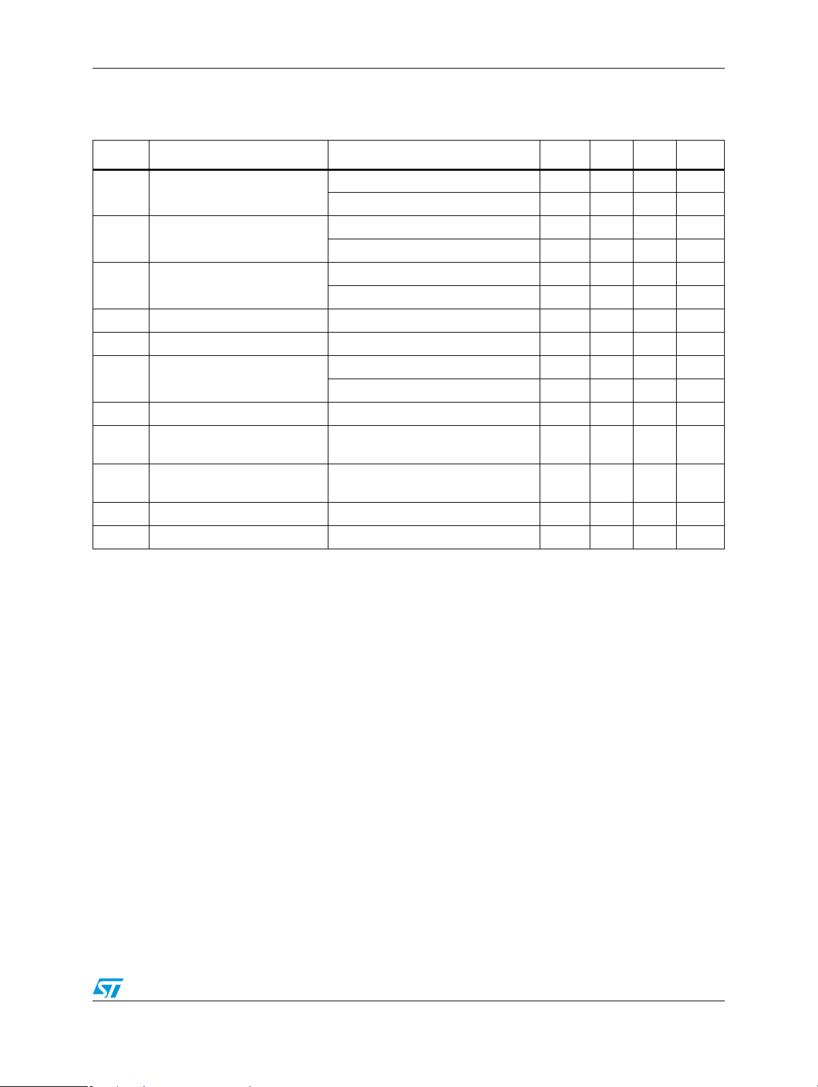
VI = 4.8 V, CI = CO =10 µF, TA = -40 to 125 °C, unless otherwise specified.
Table 5. Electrical characteristics of LD1085#18
Symbol Parameter Test condition Min. Typ. Max. Unit
V
ΔV
ΔV
V
Output voltage
O
Line regulation
O
Load regulation
O
Dropout voltage IO = 3 A 1.3 1.5 V
d
Quiescent current VI ≤ 30 V 5 10 mA
I
q
I
Short circuit current
sc
(1)
Thermal regulation T
SVR Supply voltage rejection
eN
RMS output noise voltage (% of
)
V
O
IO = 0 mA, TJ = 25°C 1.782 1.8 1.818 V
= 0 to 3 A, VI = 3.4 to 30 V 1.764 1.8 1.836 V
I
O
I
= 0 mA, VI = 3.4 to 18 V TJ = 25°C 0.2 4 mV
O
= 0 mA, VI = 3.4 to 15 V 0.4 4 mV
I
O
I
= 0 to 3 A, TJ = 25°C 2 10 mV
O
I
= 0 to 3 A 4 20 mV
O
V
- VO = 5 V 3.2 4.5 A
I
- VO = 25 V 0.2 0.5 A
V
I
= 25°C, 30 ms pulse 0.008 0.04 %/W
A
f = 120 Hz, C
VI = 7.5 ± 3 V
= 25°C, f =10 Hz to 10 kHz 0.003 %
T
A
= 25 µF, IO = 3 A
O
60 72 dB
S Temperature stability 0.5 %
S Long term stability T
1. See short-circuit current curve for available output current at fixed dropout.
= 125°C, 1000 Hrs 0.5 %
A
8/28 Doc ID 6738 Rev 25
LD1085xx Electrical characteristics
VI = 5.5 V, CI = CO =10 µF, TA = -40 to 125 °C, unless otherwise specified.
Table 6. Electrical characteristics of LD1085#25
Symbol Parameter Test condition Min. Typ. Max. Unit
V
ΔV
ΔV
V
Output voltage
O
Line regulation
O
Load regulation
O
Dropout voltage IO = 3 A 1.3 1.5 V
d
Quiescent current VI ≤ 30 V 5 10 mA
I
q
I
Short circuit current
sc
(1)
Thermal regulation T
SVR Supply voltage rejection
eN
RMS output noise voltage (%
)
of V
O
IO = 0 mA, TJ = 25°C 2.475 2.5 2.525 V
= 0 to 3 A, VI = 4.1 to 30 V 2.45 2.5 2.55 V
I
O
I
= 0 mA, VI = 4.1 to 18 V, TJ = 25°C 0.2 4 mV
O
= 0 mA, VI = 4.1 to 18 V 0.4 4 mV
I
O
I
= 0 to 3 A, TJ = 25°C 2 10 mV
O
I
= 0 to 3 A 4 20 mV
O
V
- VO = 5 V 3.2 4.5 A
I
- VO = 25 V 0.2 0.5 A
V
I
= 25°C, 30ms pulse 0.008 0.04 %/W
A
f = 120 Hz, C
VI = 7.5 ± 3 V
= 25°C, f =10 Hz to 10 kHz 0.003 %
T
A
= 25µF, IO = 3 A
O
60 72 dB
S Temperature stability 0.5 %
S Long term stability T
1. See short-circuit current curve for available output current at fixed dropout.
= 125°C, 1000 Hrs 0.5 %
A
Doc ID 6738 Rev 25 9/28
 Loading...