

3 A low-drop, adjustable positive voltage regulator
Features
■ Typical dropout 1.3 V (at 3 A)
■ Three terminal adjustable output voltage
■ Guaranteed output current up to 3 A
■ Output tolerance ± 2 % at 25 °C and ± 3 % in
full temperature range
■ Internal power and thermal limit
■ Wide operating temperature range -40 °C to
125 °C
■ Package available: DPAK
■ Pinout compatibility with standard adjustable
VREG
Description
LD1085CXX
DPAK
The LD1085C is a low drop voltage regulator able
to provide up to 3 A of output current. Dropout is
guaranteed at a maximum of 1.5 V at the
maximum output current, decreasing at lower
loads. The LD1085C is pin to pin compatible with
the older 3-terminal adjustable regulators, but has
better performances in term of drop and output
tolerance.
A 2.85 V output version is suitable for SCSI-2
active termination. Unlike PNP regulators, where
a part of the output current is wasted as quiescent
current, the LD1085C quiescent current flows into
the load, so increase efficiency. Only a 10 µF
minimum capacitor is need for stability.
The device is supplied in DPAK. On chip trimming
allows the regulator to reach a very tight output
voltage tolerance, within ± 2 % at 25 °C.
Table 1. Device summary
Order codes Packages
LD1085CDT-R DPAK (tape and reel)
April 2008 Rev 8 1/16
www.st.com
16

Contents LD1085CXX
Contents
1 Diagram . . . . . . . . . . . . . . . . . . . . . . . . . . . . . . . . . . . . . . . . . . . . . . . . . . . 3
2 Pin configuration . . . . . . . . . . . . . . . . . . . . . . . . . . . . . . . . . . . . . . . . . . . 4
3 Maximum ratings . . . . . . . . . . . . . . . . . . . . . . . . . . . . . . . . . . . . . . . . . . . . 5
4 Schematic application . . . . . . . . . . . . . . . . . . . . . . . . . . . . . . . . . . . . . . . 6
5 Electrical characteristics . . . . . . . . . . . . . . . . . . . . . . . . . . . . . . . . . . . . . 7
6 Typical application . . . . . . . . . . . . . . . . . . . . . . . . . . . . . . . . . . . . . . . . . . 8
7 Package mechanical data . . . . . . . . . . . . . . . . . . . . . . . . . . . . . . . . . . . . 12
8 Revision history . . . . . . . . . . . . . . . . . . . . . . . . . . . . . . . . . . . . . . . . . . . 15
2/16
LD1085CXX Diagram
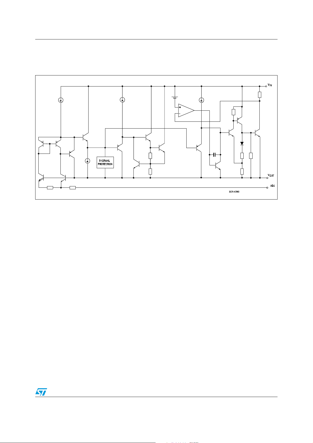
1 Diagram
Figure 1. Schematic diagram
3/16
Pin configuration LD1085CXX
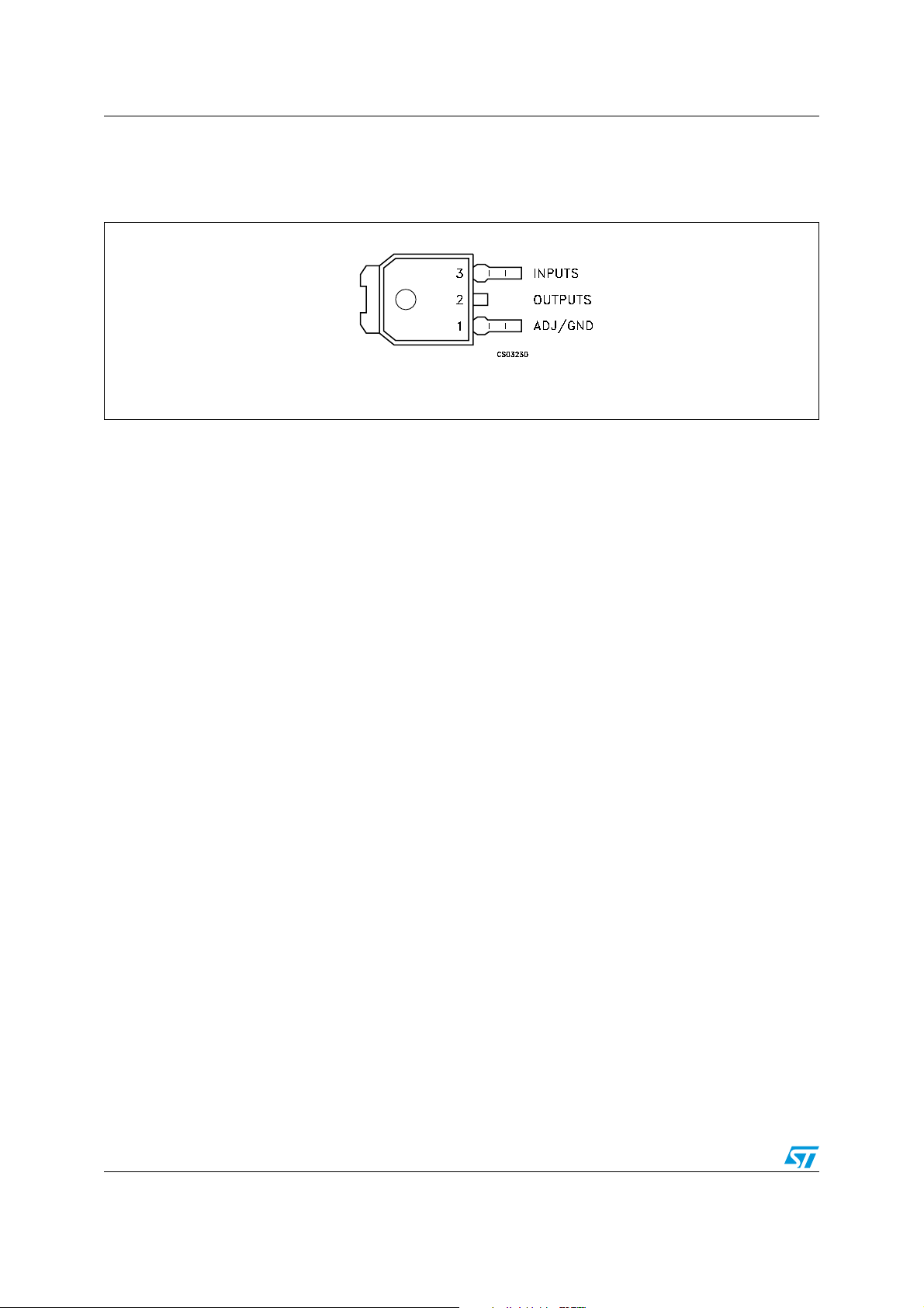
2 Pin configuration
Figure 2. Pin connections (top view)
DPAK
4/16
LD1085CXX Maximum ratings
3 Maximum ratings
Table 2. Absolute maximum ratings
Symbol Parameter Value Unit
DC input voltage 30 V
Output current Internally limited
Power dissipation Internally limited
Storage temperature range -55 to +150 °C
Operating junction temperature range -40 to +125 °C
T
P
T
V
I
I
O
D
STG
OP
Note: Absolute maximum ratings are those values beyond which damage to the device may occur.
Functional operation under these condition is not implied.
Table 3. Thermal data
Symbol Parameter DPAK Unit
R
R
thJC
thJA
Thermal resistance junction-case 3 °C/W
Thermal resistance junction-ambient 62.5 °C/W
5/16
 Loading...