

ST LD1085 User Manual
查询LD1085供应商
LD1085
SERIES
3A LOW DROP POSITIVE VOLTAGE
REGULATOR ADJUSTABLE AND FIXED
■ TYPICAL DROPOUT 1.3V (AT 3A)
■ THREE TERMINAL AD JUSTABLE OR FIXED
OUTPUT VOLTAGE 1.5V , 1.8V, 2.5V, 2.85V,
3.3V , 3.6V, 5V, 8V, 9V, 12V.
■ GUARANTEED OUTPUT CURRENT UP TO
3A
■ OUPUT TOLERANCE ±1% AT 25°C AND
±2% IN FULL TEMPERATURE RANGE
■ INTERNAL POWER AND THERMAL LIMIT
■ WIDE OPERATING TEMPERATURE RANGE
-40°C TO 125°C
■ PACKAGE AVAILABLE: TO-220, TO-220FP
2
D
PAK, D2PAK/A
■ PINOUT COMPATIBILITY WITH STANDARD
ADJUSTABLE VREG
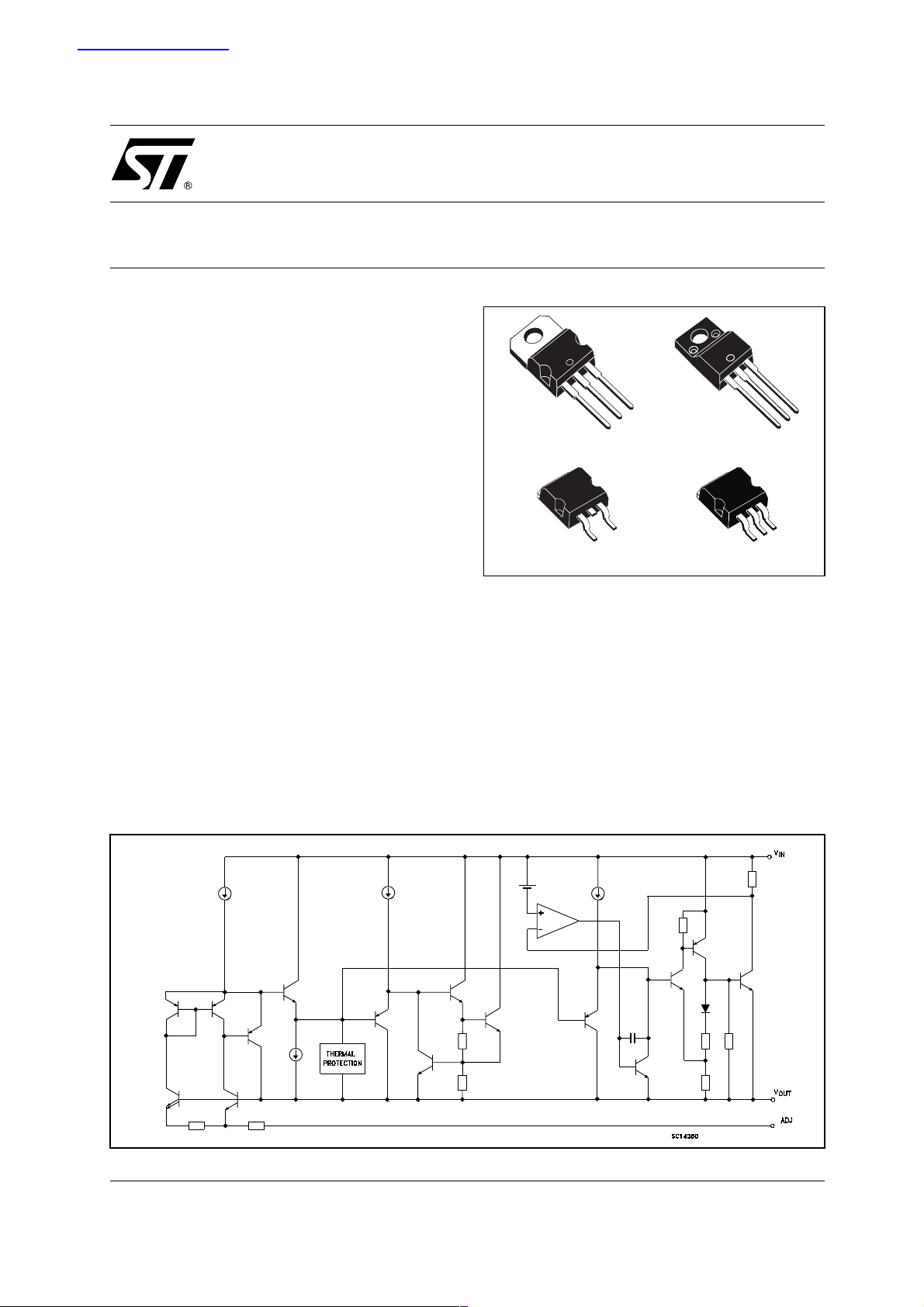
DESCRIPTION
The LD1085 is a LOW DROP Voltage Regulator
able to provide up to 3A of Output Current.
Dropout is guaran teed at a maximum o f 1.2V at
the maximum output current, decreas ing at lower
loads. The LD1085 is pin to pin compat ible with
the older 3-terminal adjustable regulators, but has
better performances in term of drop and output
tolerance.
TO-220
D2PAK D2PAK/A
TO-220FP
A 2.85V output version is suitable for SCSI-2
active termination. Unlike PNP regulators, where
a part of the output current is wasted as quiescent
current, the LD1085 quiescent current flows into
the load, so increase efficiency. Only a 10µF
minimum capacitor is need for stability.
The device is supplied in TO-220, TO-220FP,
2
D
PAK and D2PAK/A. On chip t rimming allows the
regulator to reach a very tight output voltage
tolerance, within ±1% at 25°C.
Figure 1: Schematic Diagram
Rev. 14
1/19March 2005
LD1085 SERIES
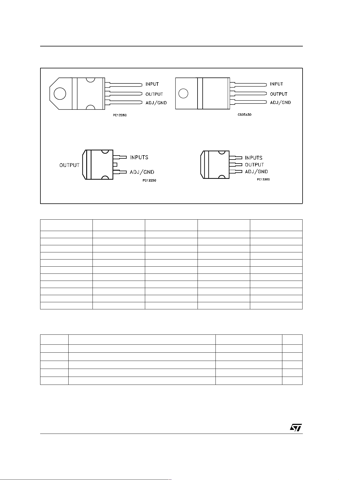
Figure 2: Pin Connec tion (top view)
TO-220 TO-220FP
2
D
PAK D2PAK/A
Table 1: Order Codes
TO-220 TO-220FP
2
PAK (*) D2PAK/A (*)
D
LD1085V15 LD1085P15 LD1085D2T15 LD1085D2M15 1.5 V
LD1085V18 LD1085P18 LD1085D2T18 LD1085D2M18 1.8 V
LD1085V25 LD1085P25 LD1085D2T25 LD1085D2M25 2.5 V
LD1085V28 LD1085P28 LD1085D2T28 LD1085D2M28 2.85 V
LD1085V33 LD1085P33 LD1085D2T33 LD1085D2M33 3.3 V
LD1085V36 LD1085P36 LD1085D2T36 LD1085D2M36 3.6 V
LD1085V50 LD1085P50 LD1085D2T50 LD1085D2M50 5.0 V
LD1085V80 LD1085P80 LD1085D2T80 LD1085D2M80 8.0 V
LD1085V90 LD1085P90 LD1085D2T90 LD1085D2M90 9.0 V
LD1085V12 LD1085P12 LD1085D2T12 LD1085D2M12 12.0 V
LD1085V LD1085P LD1085D2T LD1085D2M ADJ
(*) Avai l abl e in Tape & Reel with the suffix "R" for fixed ve rsion and "-R" for adj ustable version.
OUTPUT VOLTAGE
Table 2: Absolute Maximum Ratings
Symbol Parameter Value Unit
V
I
P
T
T
DC Input Voltage
I
Output Current
O
Power Dissipation
D
Storage Temperature Range
stg
Operating Junction Temperature Range
op
30 V
Internally Limited mA
Internally Limited mW
-55 to +150 °C
-40 to +125 °C
Absolute Maximum Ratings are those values beyond which damage to the device may occur. Functional operation under these condition is
not implied.
2/19
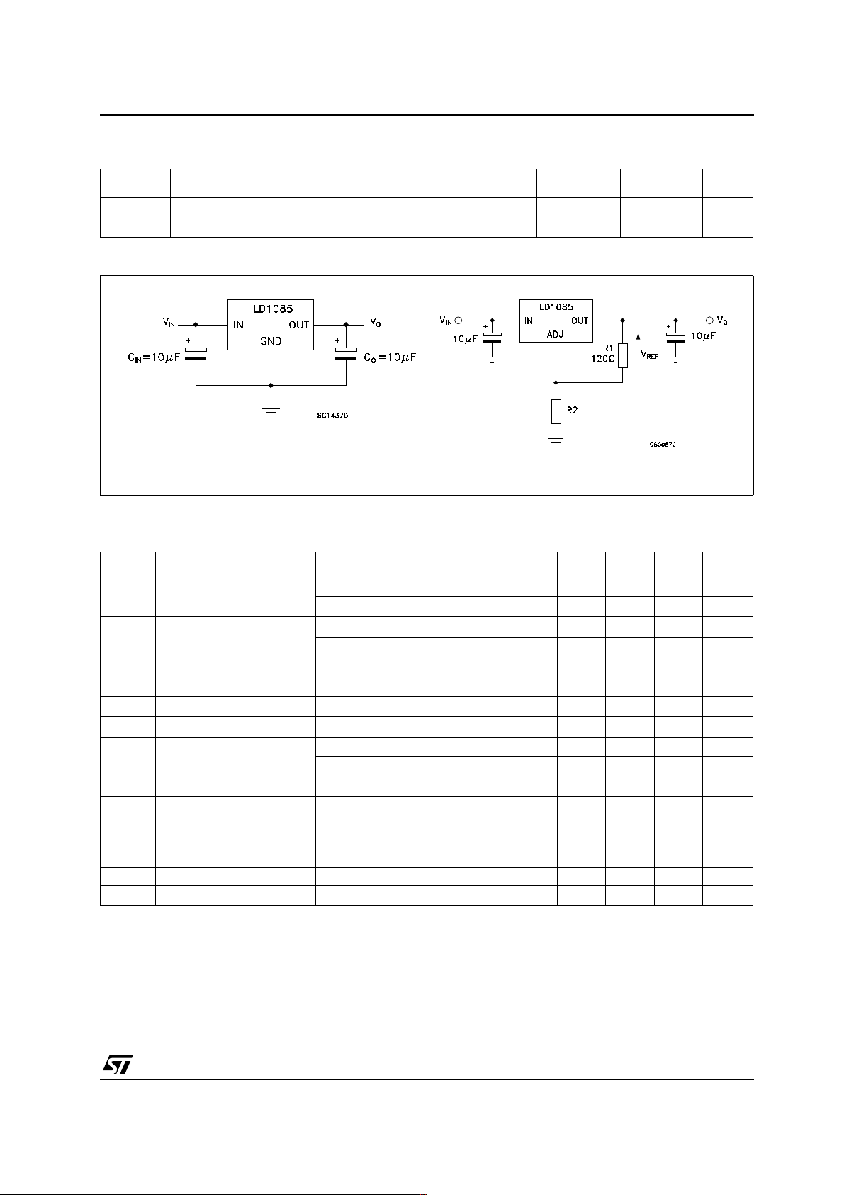
Table 3: Thermal Data
LD1085 SERIES
Symbol Parameter TO-220
R
thj-case
R
thj-amb
Thermal Resistance Junction-case
Thermal Resistance Junction-ambient
33°C/W
50 62.5 °C/W
2
PAK
D
Unit
Figure 3: Applica tion Circuits
R
2
(1 + )
R
1
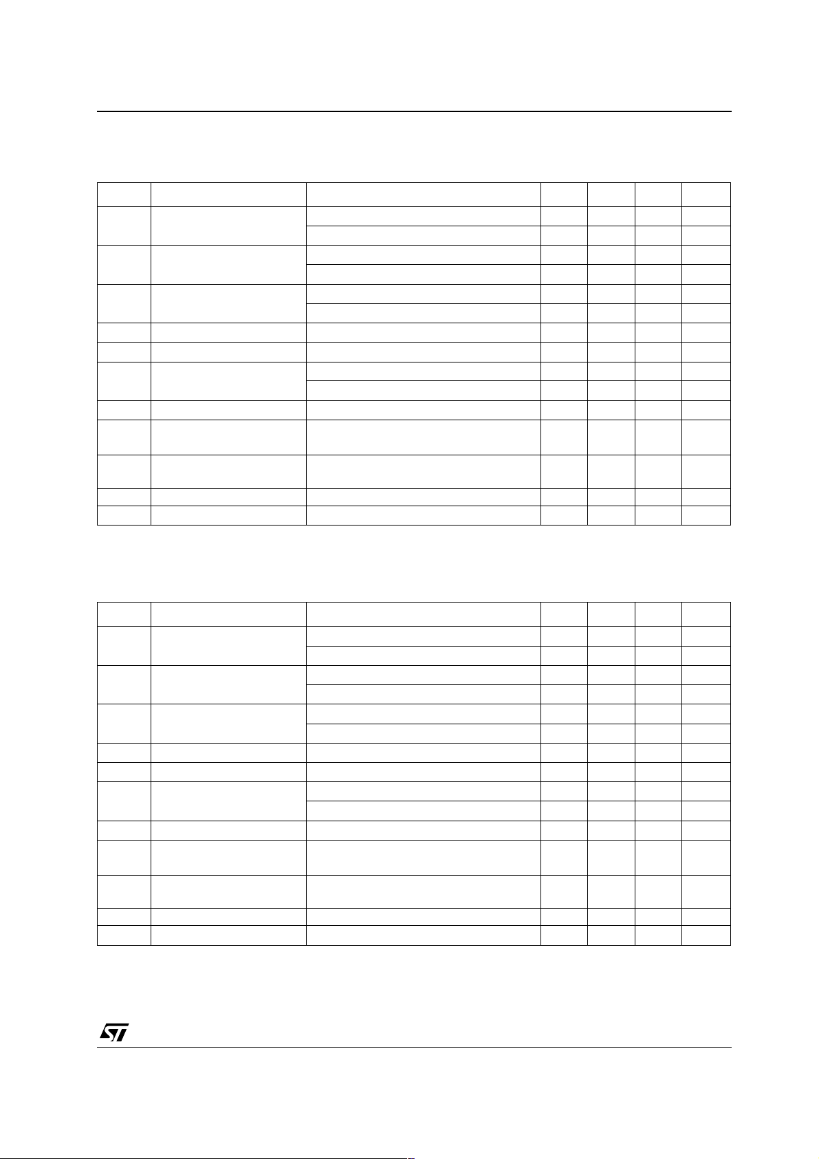
Table 4: Electrical Characteristics Of LD1085#15 (V
VO = V
REF
=4.5V, CI = CO =10µF, TA = -40 to 125°C, unless
I
otherwise specified.)
Symbol Parameter Test Conditions Min. Typ. Max. Unit
V
Output Voltage IO = 0 mA TJ = 25°C 1.485 1.5 1.515 V
O
= 0 to 5AVI = 3.1 to 30V (note 1) 1.47 1.5 1.53 V
I
O
∆V
∆V
SVR Supply Voltage Rejection f = 120 Hz, C
Line Regulation IO = 0 mA VI = 3.1 to 18V TJ = 25°C 0.2 4 mV
O
= 0 mA VI = 3.1 to 15V 0.4 4 mV
I
O
Load Regulation IO = 0 to 3ATJ = 25°C 2 10 mV
O
= 0 to 3A 4 20 mV
I
O
V
Dropout Voltage IO =3 A 1.3 1.5 V
d
Quiescent Current VI ≤ 30V 5 10 mA
I
q
Short Circuit Current VI - VO = 5V 3.2 4.5 A
I
sc
- VO = 25V 0.2 0.5 A
V
I
Thermal Regulation T
eN RMS Output Noise Voltage
(% of V
)
O
= 25°C, 30ms pulse 0.008 0.04 %/W
A
= 25 µF, IO = 3A
= 7.5 ± 3V
V
I
T
= 25°C f =10Hz to 10KHz 0.003 %
A
O
60 72 dB
S Temperature Stability 0.5 %
S Long Term Stability TA = 125°C 1000Hrs 0.5 %
NOTE 1: Se e short-circuit curr ent curve for available output cur rent at fixed dropout.
3/19
LD1085 SERIES
Table 5: Electrical Characteristics Of LD1085#18 (VI=4.8V, CI = CO =10µF, TA = -40 to 125°C, unless
otherwise specified.)
Symbol Parameter Test Conditions Min. Typ. Max. Unit
V
Output Voltage IO = 0 mA TJ = 25°C 1.782 1.8 1.818 V
O
= 0 to 5AVI = 3.4 to 30V (note 1) 1.764 1.8 1.836 V
I
O
∆V
∆V
SVR Supply Voltage Rejection f = 120 Hz, C
Line Regulation IO = 0 mA VI = 3.4 to 18V TJ = 25°C 0.2 4 mV
O
= 0 mA VI = 3.4 to 15V 0.4 4 mV
I
O
Load Regulation IO = 0 to 3ATJ = 25°C 2 10 mV
O
= 0 to 3A 4 20 mV
I
O
Dropout Voltage IO =3 A 1.3 1.5 V
V
d
I
Quiescent Current VI ≤ 30V 5 10 mA
q
Short Circuit Current VI - VO = 5V 3.2 4.5 A
I
sc
- VO = 25V 0.2 0.5 A
V
I
Thermal Regulation T
eN RMS Output Noise Voltage
(% of V
)
O
= 25°C, 30ms pulse 0.008 0.04 %/W
A
= 25 µF, IO = 3A
V
= 7.5 ± 3V
I
T
= 25°C f =10Hz to 10KHz 0.003 %
A
O
60 72 dB
S Temperature Stability 0.5 %
S Long Term Stability TA = 125°C 1000Hrs 0.5 %
NOTE 1: Se e short-circuit curr ent curve for available output cur rent at fixed dropout.
Table 6: Electrical Characteristics Of LD1085#25 (VI=5.5V, CI = CO =10µF, TA = -40 to 125°C, unless
otherwise specified.)
Symbol Parameter Test Conditions Min. Typ. Max. Unit
V
Output Voltage IO = 0 mA TJ = 25°C 2.475 2.5 2.525 V
O
I
= 0 to 3AVI = 4.1 to 30V (note 1) 2.45 2.5 2.55 V
O
∆V
∆V
SVR Supply Voltage Rejection f = 120 Hz, C
Line Regulation IO = 0 mA VI = 4.1 to 18V TJ = 25°C 0.2 4 mV
O
= 0 mA VI = 4.1 to 18V 0.4 4 mV
I
O
Load Regulation IO = 0 to 3ATJ = 25°C 2 10 mV
O
I
= 0 to 3A 4 20 mV
O
Dropout Voltage IO =3 A 1.3 1.5 V
V
d
Quiescent Current VI ≤ 30V 5 10 mA
I
q
Short Circuit Current VI - VO = 5V 3.2 4.5 A
I
sc
- VO = 25V 0.2 0.5 A
V
I
Thermal Regulation T
eN RMS Output Noise Voltage
(% of V
)
O
= 25°C, 30ms pulse 0.008 0.04 %/W
A
= 25 µF, IO = 3A
V
= 7.5 ± 3V
I
T
= 25°C f =10Hz to 10KHz 0.003 %
A
O
60 72 dB
S Temperature Stability 0.5 %
S Long Term Stability T
= 125°C 1000Hrs 0.5 %
A
NOTE 1: Se e short-circuit curr ent curve for available output cur rent at fixed dropout.
4/19
LD1085 SERIES
Table 7: Electrical Characteristics Of LD1085#285 (VI=5.85V, CI = CO =10µF, TA = -40 to 125°C,
unless otherwise specified.)
Symbol Parameter Test Conditions Min. Typ. Max. Unit
V
Output Voltage IO = 0 mA TJ = 25°C 2.821 2.85 2.879 V
O
= 0 to 3AVI = 4.5 to 30V (note 1) 2.793 2.85 2.907 V
I
O
∆V
∆V
SVR Supply Voltage Rejection f = 120 Hz, C
Line Regulation IO = 0 mA VI = 4.5 to 18V TJ = 25°C 0.2 6 mV
O
= 0 mA VI = 4.5 to 18V 0.5 6 mV
I
O
Load Regulation IO = 0 to 3ATJ = 25°C 3 15 mV
O
= 0 to 3A 7 20 mV
I
O
Dropout Voltage IO =3 A 1.3 1.5 V
V
d
I
Quiescent Current VI ≤ 30V 5 10 mA
q
Short Circuit Current VI - VO = 5V 3.2 4.5 A
I
sc
- VO = 25V 0.2 0.5 A
V
I
Thermal Regulation T
eN RMS Output Noise Voltage
(% of V
)
O
= 25°C, 30ms pulse 0.008 0.04 %/W
A
= 25 µF, IO = 3A
V
= 7.85 ± 3V
I
T
= 25°C f =10Hz to 10KHz 0.003 %
A
O
60 72 dB
S Temperature Stability 0.5 %
S Long Term Stability TA = 125°C 1000Hrs 0.5 %
NOTE 1: Se e short-circuit curr ent curve for available output cur rent at fixed dropout.
Table 8: Electrical Characteristics Of LD1085#33 (VI=6.3V, CI = CO =10µF, TA = -40 to 125°C, unless
otherwise specified.)
Symbol Parameter Test Conditions Min. Typ. Max. Unit
V
Output Voltage IO = 0 mA TJ = 25°C 3.267 3.3 3.333 V
O
I
= 0 to 3AVI = 4.9 to 30V (note 1) 3.234 3.35 3.366 V
O
∆V
∆V
SVR Supply Voltage Rejection f = 120 Hz, C
Line Regulation IO = 0 mA VI = 4.9 to 18V TJ = 25°C 0.5 6 mV
O
= 0 mA VI = 4.9 to 18V 1 6 mV
I
O
Load Regulation IO = 0 to 3ATJ = 25°C 3 15 mV
O
I
= 0 to 3A 7 20 mV
O
Dropout Voltage IO =3 A 1.3 1.5 V
V
d
Quiescent Current VI ≤ 30V 5 10 mA
I
q
Short Circuit Current VI - VO = 5V 3.2 4.5 A
I
sc
- VO = 25V 0.2 0.5 A
V
I
Thermal Regulation T
eN RMS Output Noise Voltage
(% of V
)
O
= 25°C, 30ms pulse 0.008 0.04 %/W
A
= 25 µF, IO = 5A
V
= 8.3 ± 3V
I
T
= 25°C f =10Hz to 10KHz 0.003 %
A
O
60 72 dB
S Temperature Stability 0.5 %
S Long Term Stability T
= 125°C 1000Hrs 0.5 %
A
NOTE 1: Se e short-circuit curr ent curve for available output cur rent at fixed dropout.
5/19

LD1085 SERIES
Table 9: Electrical Characteristics Of LD1085#36 (VI=6.6V, CI = CO =10µF, TA = -40 to 125°C, unless
otherwise specified.)
Symbol Parameter Test Conditions Min. Typ. Max. Unit
V
Output Voltage IO = 0 mA TJ = 25°C 3.564 3.6 3.636 V
O
= 0 to 3AVI = 5.2 to 30V (note 1) 3.528 3.6 3.672 V
I
O
∆V
∆V
SVR Supply Voltage Rejection f = 120 Hz, C
Line Regulation IO = 0 mA VI = 5.2 to 18V TJ = 25°C 0.5 10 mV
O
= 0 mA VI = 5.2 to 18V 1 10 mV
I
O
Load Regulation IO = 0 to 3ATJ = 25°C 3 15 mV
O
= 0 to 3A 7 20 mV
I
O
Dropout Voltage IO =3 A 1.3 1.5 V
V
d
I
Quiescent Current VI ≤ 30V 5 10 mA
q
Short Circuit Current VI - VO = 5V 3.2 4.5 A
I
sc
- VO = 25V 0.2 0.5 A
V
I
Thermal Regulation T
eN RMS Output Noise Voltage
(% of V
)
O
= 25°C, 30ms pulse 0.008 0.04 %/W
A
= 25 µF, IO = 3A
V
= 8.6 ± 3V
I
T
= 25°C f =10Hz to 10KHz 0.003 %
A
O
60 72 dB
S Temperature Stability 0.5 %
S Long Term Stability TA = 125°C 1000Hrs 0.5 %
NOTE 1: Se e short-circuit curr ent curve for available output cur rent at fixed dropout.
Table 10: Electrical Characteristics Of LD1085#50 (VI=8V, CI = CO =10µF, TA = -40 to 125°C, unless
otherwise specified.)
Symbol Parameter Test Conditions Min. Typ. Max. Unit
V
Output Voltage IO = 0 mA TJ = 25°C 4.95 5 5.05 V
O
I
= 0 to 3AVI = 6.6 to 30V (note 1) 4.9 5 5.1 V
O
∆V
∆V
SVR Supply Voltage Rejection f = 120 Hz, C
Line Regulation IO = 0 mA VI = 6.6 to 20V TJ = 25°C 0.5 10 mV
O
= 0 mA VI = 6.6 to 20V 1 10 mV
I
O
Load Regulation IO = 0 to 3ATJ = 25°C 5 10 mV
O
I
= 0 to 3A 10 35 mV
O
Dropout Voltage IO =3 A 1.3 1.5 V
V
d
Quiescent Current VI ≤ 30V 5 10 mA
I
q
Short Circuit Current VI - VO = 5V 3.2 4.5 A
I
sc
- VO = 25V 0.2 0.5 A
V
I
Thermal Regulation T
eN RMS Output Noise Voltage
(% of V
)
O
= 25°C, 30ms pulse 0.008 0.04 %/W
A
= 25 µF, IO = 3A
V
= 10 ± 3V
I
T
= 25°C f =10Hz to 10KHz 0.003 %
A
O
60 72 dB
S Temperature Stability 0.5 %
S Long Term Stability T
= 125°C 1000Hrs 0.5 %
A
NOTE 1: Se e short-circuit curr ent curve for available output cur rent at fixed dropout.
6/19
 Loading...