

查询LD1084供应商
REGULATOR ADJUSTABLE AND FIXED
■ TYPICAL DROPOUT 1.3V (AT 5A)
■ THREE TERMINAL ADJUSTABLE OR FIXED
OUTPUT VOLTAGE 1.5, 1.8V , 2.5V, 2.85V,
3.3V,3.6V,5V,8V,9V,12V.
■ GUARANTEED OUTPUT CURRENT UP TO
5A
■ OUPUT TOLERANCE ±1% AT 25°C AND
±2% IN FU LL TEMPERATURE RANGE
■ INTERNAL POWER AND THERMAL LIMIT
■ WIDE OPERATING TEMPERATURE RANGE
-40°C TO 125°C
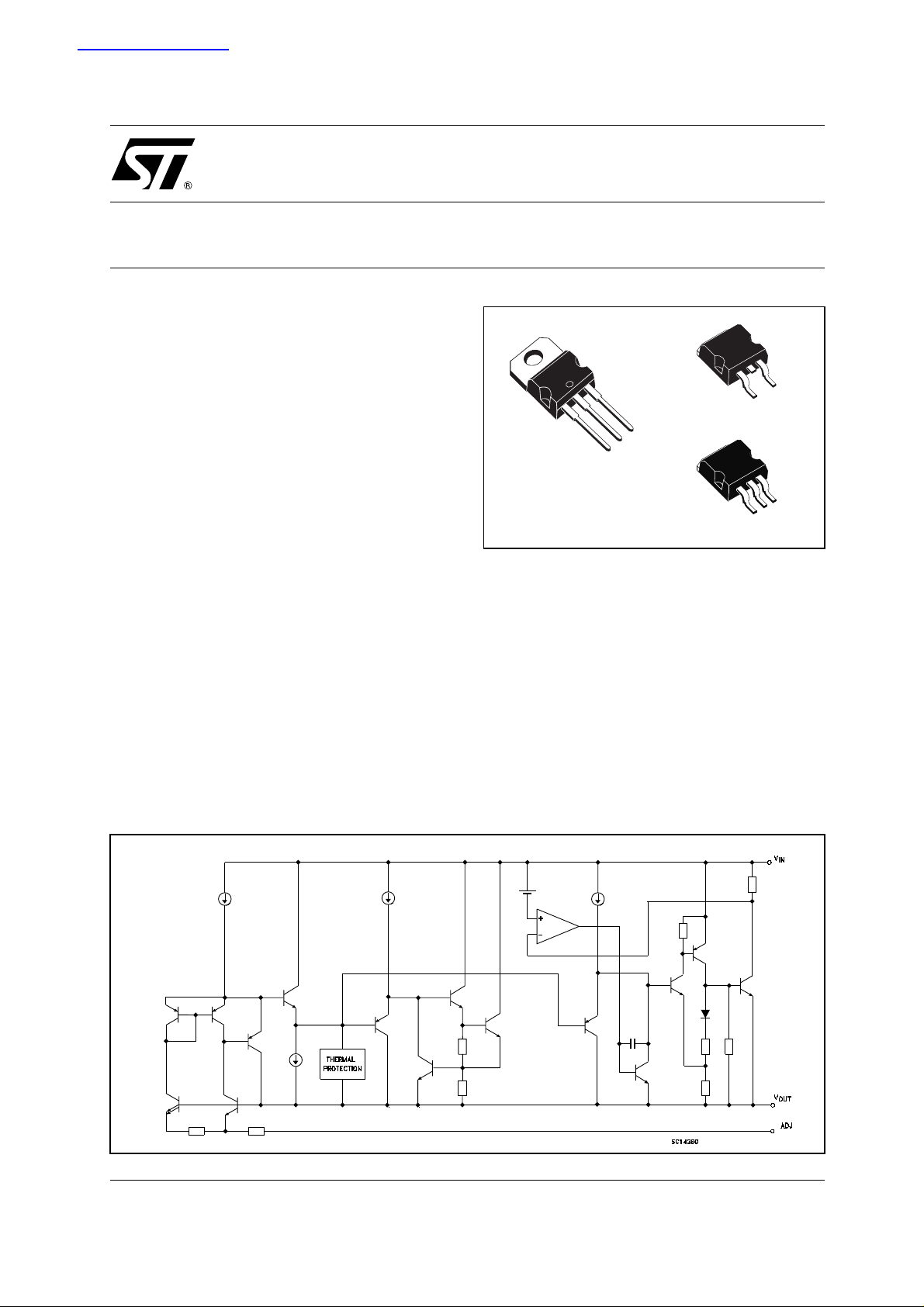
■ PACKAGE AVAILABLE : TO-220,D
2
D
PAK/A
■ PINOUT COMPATIBILITY WITH STANDARD
ADJUSTABLE VREG
DESCRIPTION
The LD1084 is a LOW DROP Voltage Regulator
able to provide up to 5A of Output Current.
Dropout is guaran teed at a maxim um of 1.5V at
the maximum output current, decreasing at lower
loads. The LD1084 is pin to pin compatible with
the older 3-terminal adj us tab le regulators, but has
better performances in term of drop and output
tolerance .
LD1084
SERIES
5A LOW DROP POSITIVE VOLTAGE
D2PAK
TO-220
2
PAK,
A 2.85V output version is suitable for SCSI-2
active termination. Unlike PNP regulato rs, where
a part of the output current is wasted as quiescent
current, the LD1084 quiescent current flows into
the load, so increase efficiency. Only a 10µF
minimum capac it or is need for stability.
The device is supplied i n T O-220, D
2
D
PAK/A. On chiptrimming allows the regulator to
reach a very tight output voltage tolerance, within
±1% at 25°C.
2
D
PAK/A
2
PAK a nd
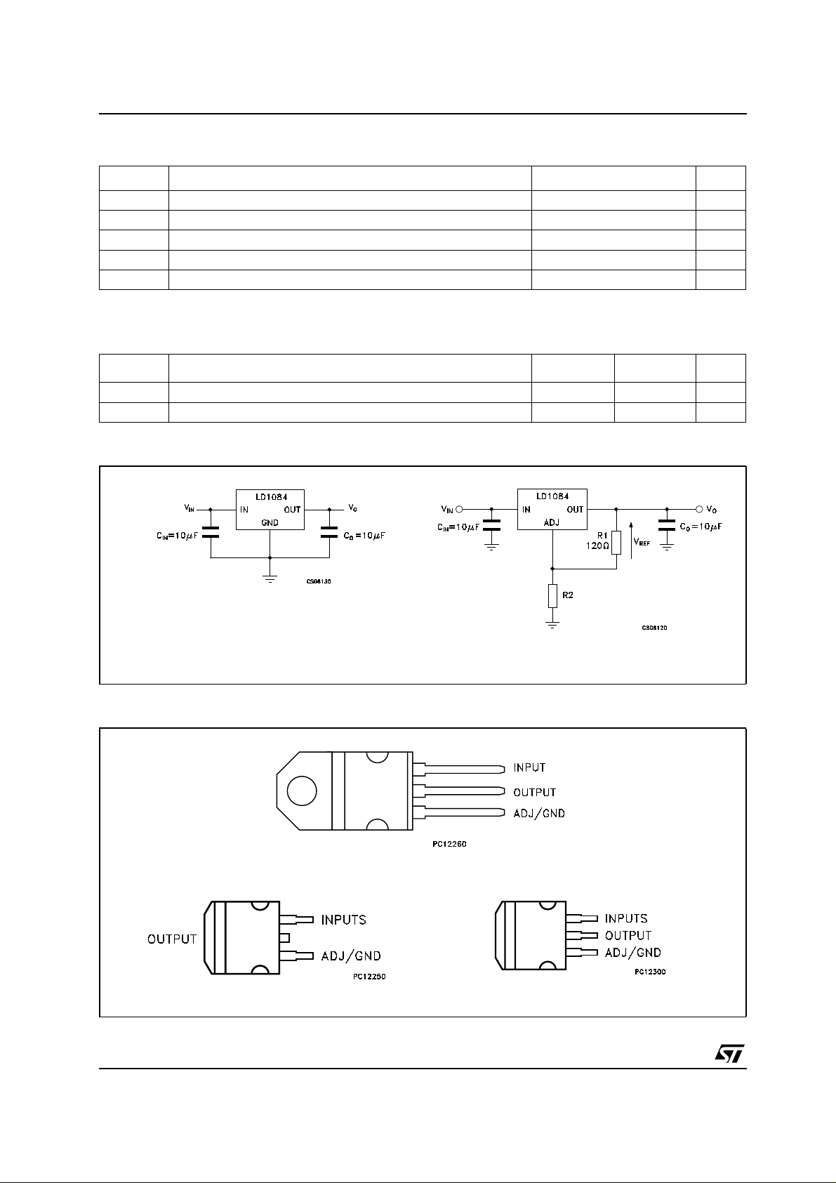
SCHEMATIC DIAGRAM
1/18May 2003
LD1084 SERIES
ABSOLUTE MAXIMUM RATINGS
Symbol Parameter² Value Unit
V
I
P
T
T
Absolute Maximum Ratings are those values beyond which damage to the device may occur. Functional operation under these condition is
not implied.
THERMAL DATA
DC Input Voltage
I
Output Current
O
Power Dissipation
D
Storage Temperature Range
stg
Operating Junction Temperature Range
op
30 V
Internally Limited mA
Internally Limited mW
-55 to +150 °C
-40 to +125 °C
Symbol Parameter TO-220
R
thj-case
R
thj-amb
Thermal Resistance Junction-case
Thermal Resistance Junction-ambient
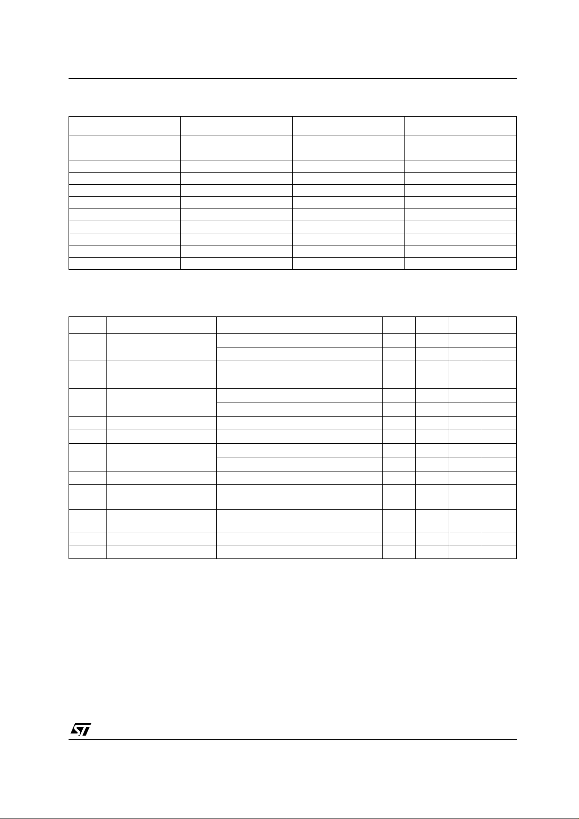
APPLICATION CIRCUITS
R
VO=V
REF
2
(1 + )
R
1
CONNECTION DIAGRAM (top view)
2
PAK
D
Unit
3 3 °C/W
50 62.5 °C/W
2/18
TO-220
2
PAK D2PAK/A
D
ORDERING CODES
LD1084 SE RIE S
TYPE
2
PAK (*) D2PAK/A
D
OUTPUT VOLTAGE
LD1084V15 LD1084D2T15 LD1084D2M15 1.5 V
LD1084V18 LD1084D2T18 LD1084D2M18 1.8 V
LD1084V25 LD1084D2T25 LD1084D2M25 2.5 V
LD1084V28 LD1084D2T28 LD1084D2M28 2.85 V
LD1084V33 LD1084D2T33 LD1084D2M33 3.3 V
LD1084V36 LD1084D2T36 LD1084D2M36 3.6 V
LD1084V50 LD1084D2T50 LD1084D2M50 5.0 V
LD1084V80 LD1084D2T80 LD1084D2M80 8.0 V
LD1084V90 LD1084D2T90 LD1084D2M90 9.0 V
LD1084V120 LD1084D2T120 LD1084D2M120 12.0 V
LD1084V LD1084D2T LD1084D2M ADJ
(*) Available in Tape & Reel with the suffix "R" for fixed versions and "-R" for adjustable version
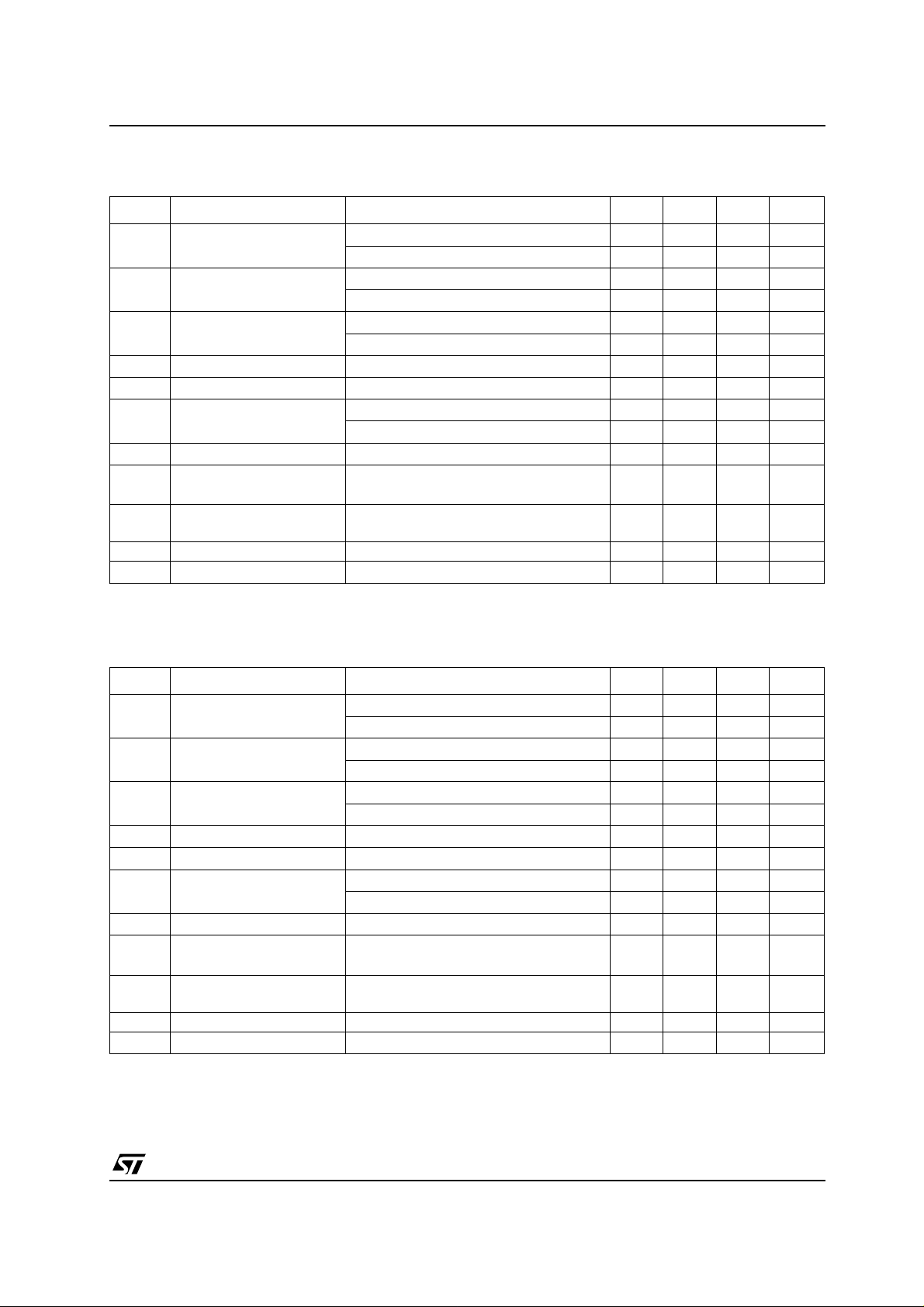
LECTRICAL CHARACTERISTICS O F L D1084#15 (VI=4.5V, CI=CO=10µF, TA= -40 to 125°C, unless
otherwise specified.)
Symbol Parameter Test Conditions Min. Typ. Max. Unit
V
Output Voltage IO=0mA TJ= 25°C 1.485 1.5 1.515 V
O
=0to5A VI= 3.1 to 30V (note 1) 1.47 1.5 1.53 V
I
O
∆V
∆V
SVR Supply Voltage Rejection f = 120 Hz, C
NOTE 1: See short-circuit current curve for available output current at fixed dropout.
Line Regulation IO=0mA VI= 3.1 to 18V TJ= 25°C 0.5 6 mV
O
=0mA VI= 3.1 to 15V 0.1 6 mV
I
O
Load Regulation IO=0to5A TJ= 25°C 3 15 mV
O
=0to5A 7 20 V
I
O
Dropout Voltage IO=5 A 1.3 1.5 V
V
d
Quiescent Current VI≤ 30V 5 10 mA
I
q
I
Short Circuit Current VI-VO= 5V 5.5 6.5 A
sc
= 25V 0.5 0.7 A
V
I-VO
Termal Regulation T
eN RMS Output Noise Voltage
(% of V
)
O
= 25°C, 30ms pulse 0.003 0.015 %/W
A
=25µF, IO=5A
V
= 6.8 ± 3V
I
T
= 25°C f =10Hz to 10KHz 0.003 %
A
O
60 75 dB
S Temperature Stability 0.5 %
S Long Term Stability T
= 125°C 1000Hrs 0.5 %
A
3/18
LD1084 SERIES
ELECTRICAL CHARACTERISTICS OF LD1084#18 (VI=4.8V, CI=CO=10µF, TA= -40 to 125°C, unless
otherwise specified.)
Symbol Parameter Test Conditions Min. Typ. Max. Unit
V
Output Voltage IO=0mA TJ= 25°C 1.782 1.8 1.818 V
O
=0to5A VI= 3.4 to 30V (note 1) 1.764 1.8 1.836 V
I
O
∆V
∆V
SVR Supply Voltage Rejection f = 120 Hz, C
NOTE 1: See short-circuit current curve for available output current at fixed dropout.
Line Regulation IO=0mA VI= 3.4 to 18V TJ= 25°C 0.5 6 mV
O
=0mA VI= 3.4 to 15V 0.1 6 mV
I
O
Load Regulation IO=0to5A TJ= 25°C 3 15 mV
O
=0to5A 7 20 V
I
O
Dropout Voltage IO=5 A 1.3 1.5 V
V
d
Quiescent Current VI≤ 30V 5 10 mA
I
q
Short Circuit Current VI-VO= 5V 5.5 6.5 A
I
sc
= 25V 0.5 0.7 A
V
I-VO
Termal Regulation T
eN RMS Output Noise Voltage
(% of V
)
O
= 25°C, 30ms pulse 0.003 0.015 %/W
A
=25µF, IO=5A
V
= 6.8 ± 3V
I
T
= 25°C f =10Hz to 10KHz 0.003 %
A
O
60 75 dB
S Temperature Stability 0.5 %
S Long Term Stability T
= 125°C 1000Hrs 0.5 %
A
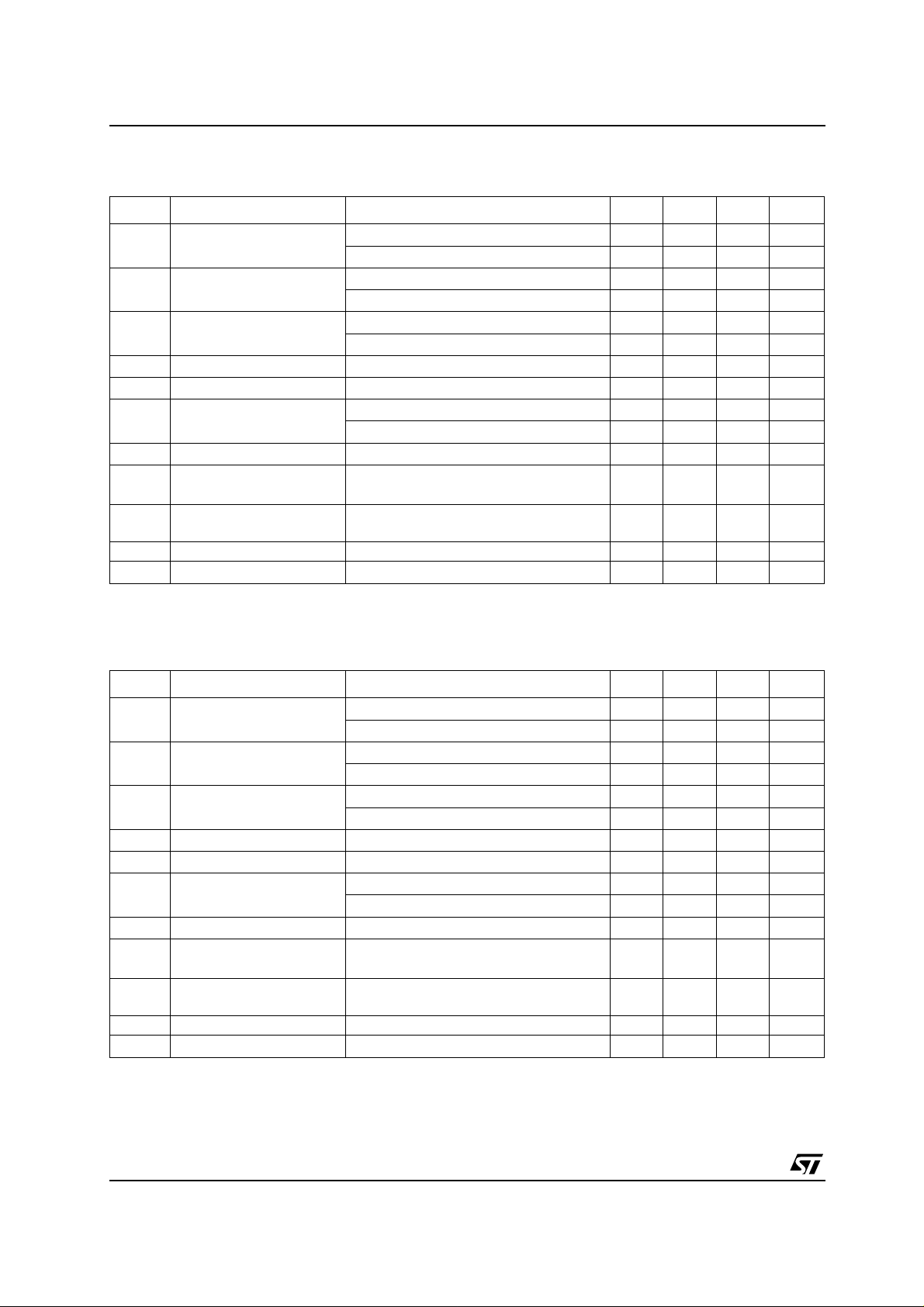
ELECTRICAL CHARACTERISTICS OF LD1084#25 (VI=5.5V, CI=CO=10µF, TA= -40 to 125°C, unless
otherwise specified.)
Symbol Parameter Test Conditions Min. Typ. Max. Unit
Output Voltage IO=0mA TJ= 25°C 2.475 2.5 2.525 V
V
O
I
=0to5A VI= 4.1 to 30V (note 1) 2.45 2.5 2.55 V
O
∆V
∆V
SVR Supply Voltage Rejection f = 120 Hz, C
NOTE 1: See short-circuit current curve for available output current at fixed dropout.
Line Regulation IO=0mA VI= 4.1 to 18V TJ= 25°C 0.5 6 mV
O
=0mA VI= 4.1 to 18V 0.1 6 mV
I
O
Load Regulation IO=0to5A TJ= 25°C 3 15 mV
O
=0to5A 7 20 V
I
O
V
Dropout Voltage IO=5 A 1.3 1.5 V
d
Quiescent Current VI≤ 30V 5 10 mA
I
q
Short Circuit Current VI-VO= 5V 5.5 6.5 A
I
sc
= 25V 0.5 0.7 A
V
I-VO
Termal Regulation T
eN RMS Output Noise Voltage
(% of V
)
O
= 25°C, 30ms pulse 0.003 0.015 %/W
A
=25µF, IO=5A
V
= 7.5 ± 3V
I
T
= 25°C f =10Hz to 10KHz 0.003 %
A
O
60 72 dB
S Temperature Stability 0.5 %
S Long Term Stability T
= 125°C 1000Hrs 0.5 %
A
4/18
LD1084 SE RIE S
ELECTRICAL CHARACTERISTICS OF LD1084#285 (VI=5.85V, CI=CO=10µF, TA= -40 to 125°C,
unless otherwise specified. )
Symbol Parameter Test Conditions Min. Typ. Max. Unit
V
Output Voltage IO=0mA TJ= 25°C 2.821 2.85 2.879 V
O
=0to5A VI= 4.5 to 30V (note 1) 2.793 2.85 2.907 V
I
O
∆V
∆V
SVR Supply Voltage Rejection f = 120 Hz, C
NOTE 1: See short-circuit current curve for available output current at fixed dropout.
Line Regulation IO=0mA VI= 4.5 to 18V TJ= 25°C 0.5 6 mV
O
=0mA VI= 4.5 to 18V 0.1 6 mV
I
O
Load Regulation IO=0to5A TJ= 25°C 3 15 mV
O
I
=0to5A 7 20 V
O
Dropout Voltage IO=5 A 1.3 1.5 V
V
d
Quiescent Current VI≤ 30V 5 10 mA
I
q
Short Circuit Current VI-VO= 5V 5.5 6.5 A
I
sc
= 25V 0.5 0.7 A
V
I-VO
Termal Regulation T
eN RMS Output Noise Voltage
(% of V
)
O
= 25°C, 30ms pulse 0.003 0.015 %/W
A
=25µF, IO=5A
V
= 7.85 ± 3V
I
T
= 25°C f =10Hz to 10KHz 0.003 %
A
O
60 72 dB
S Temperature Stability 0.5 %
S Long Term Stability T
= 125°C 1000Hrs 0.5 %
A
ELECTRICAL CHARACTERISTICS OF LD1084#33 (VI=6.3V, CI=CO=10µF, TA= -40 to 125°C, unless
otherwise specified.)
Symbol Parameter Test Conditions Min. Typ. Max. Unit
Output Voltage IO=0mA TJ= 25°C 3.267 3.3 3.333 V
V
O
=0to5A VI= 4.9 to 30V (note 1) 3.234 3.35 3.366 V
I
O
∆V
∆V
SVR Supply Voltage Rejection f = 120 Hz, C
NOTE 1: See short-circuit current curve for available output current at fixed dropout.
Line Regulation IO=0mA VI= 4.9 to 18V TJ= 25°C 0.5 6 mV
O
=0mA VI= 4.9 to 18V 0.1 6 mV
I
O
Load Regulation IO=0to5A TJ= 25°C 3 15 mV
O
=0to5A 7 20 V
I
O
Dropout Voltage IO=5 A 1.3 1.5 V
V
d
Quiescent Current VI≤ 30V 5 10 mA
I
q
Short Circuit Current VI-VO= 5V 5.5 6.5 A
I
sc
= 25V 0.5 0.7 A
V
I-VO
Termal Regulation T
eN RMS Output Noise Voltage
(% of V
)
O
= 25°C, 30ms pulse 0.003 0.015 %/W
A
=25µF, IO=5A
V
= 8.3 ± 3V
I
T
= 25°C f =10Hz to 10KHz 0.003 %
A
O
60 72 dB
S Temperature Stability 0.5 %
S Long Term Stability T
= 125°C 1000Hrs 0.5 %
A
5/18
LD1084 SERIES
ELECTRICAL CHARACTERISTICS OF LD1084#36 (VI=6.6V, CI=CO=10µF, TA= -40 to 125°C, unless
otherwise specified.)
Symbol Parameter Test Conditions Min. Typ. Max. Unit
V
Output Voltage IO=0mA TJ= 25°C 3.564 3.6 3.636 V
O
=0to5A VI= 5.2 to 30V (note 1) 3.528 3.6 3.672 V
I
O
∆V
∆V
SVR Supply Voltage Rejection f = 120 Hz, C
NOTE 1: See short-circuit current curve for available output current at fixed dropout.
Line Regulation IO=0mA VI= 5.2 to 18V TJ= 25°C 0.5 10 mV
O
=0mA VI= 5.2 to 18V 0.1 10 mV
I
O
Load Regulation IO=0to5A TJ= 25°C 3 15 mV
O
I
=0to5A 7 20 V
O
Dropout Voltage IO=5 A 1.3 1.5 V
V
d
Quiescent Current VI≤ 30V 5 10 mA
I
q
Short Circuit Current VI-VO= 5V 5.5 6.5 A
I
sc
= 25V 0.5 0.7 A
V
I-VO
Termal Regulation T
eN RMS Output Noise Voltage
(% of V
)
O
= 25°C, 30ms pulse 0.003 0.015 %/W
A
=25µF, IO=5A
V
= 8.6 ± 3V
I
T
= 25°C f =10Hz to 10KHz 0.003 %
A
O
60 72 dB
S Temperature Stability 0.5 %
S Long Term Stability T
= 125°C 1000Hrs 0.5 %
A
ELECTRICAL CHARACTERISTICS OF LD1084#5 (VI=8V, CI=CO=10µF, TA= -40 to 125°C, unless
otherwise specified.)
Symbol Parameter Test Conditions Min. Typ. Max. Unit
Output Voltage IO=0mA TJ= 25°C 4.95 5 5.05 V
V
O
=0to5A VI= 6.6 to 30V (note 1) 4.9 5 5.1 V
I
O
∆V
∆V
SVR Supply Voltage Rejection f = 120 Hz, C
NOTE 1: See short-circuit current curve for available output current at fixed dropout.
Line Regulation IO=0mA VI= 6.6 to 20V TJ= 25°C 0.5 10 mV
O
=0mA VI= 6.6 to 20V 1 10 mV
I
O
Load Regulation IO=0to5A TJ= 25°C 5 20 mV
O
I
=0to5A 10 35 V
O
Dropout Voltage IO=5 A 1.3 1.5 V
V
d
Quiescent Current VI≤ 30V 5 10 mA
I
q
Short Circuit Current VI-VO= 5V 5.5 6.5 A
I
sc
= 25V 0.5 0.7 A
V
I-VO
Termal Regulation T
eN RMS Output Noise Voltage
(% of V
)
O
= 25°C, 30ms pulse 0.003 0.015 %/W
A
=25µF, IO=5A
V
=10± 3V
I
T
= 25°C f =10Hz to 10KHz 0.003 %
A
O
60 72 dB
S Temperature Stability 0.5 %
S Long Term Stability T
= 125°C 1000Hrs 0.5 %
A
6/18
 Loading...