How it Works
Log In / Sign Up
Buy Points
How it Works
FAQ
Contact Us
Questions and Suggestions
Users
ST
Loading...
L
L9615
L9616
L9637
L9651
L9659
L9700D-E
L9733
L9758
L9805E
L9820
L9822E
L9823
L9825
L9826
L9848
L9856
L9903
L9904
L9907
L9911
L9925
L9935
L9942
L9949
L9950
L9950XP
L9951
2
L9951XP
L9952GXP
L9953
L9953LXP
L9953XP
L9954
L9954LXP
L9954XP
L9958
L9959T
L9960T
2
L9997ND
L99DZ70XP
L99DZ80EP
L99DZ81EP
L99H01
2
L99LD01
L99MC6
L99MD01
L99MD02
L99MM70XP
L99PD08
L99PM60J
L99PM62GXP
L99PM62XP
2
L99PM72PXP
L99UDL01
LCD-PDP/TV
LD1084
LD1084V
LD1085
LD1085CDT-R
LD1085D2M
LD1085D2M18R
LD1085D2M25R
LD1085D2M33R
LD1085D2M-R
LD1085D2T18R
LD1085D2T33R
LD1085D2T-R
LD1085DT15R
LD1085DT18R
LD1085DT25R
LD1085DT33R
LD1085P
LD1085PY
LD1085V
LD1085V25
LD1085V50
LD1086
2
LD1086D2M33TR
LD1086D2MTR
LD1086D2T12TR
LD1086D2T18TR
LD1086D2T25TR
LD1086D2T33TR
LD1086D2T50TR
LD1086D2TTR
LD1086DT18TR
LD1086DT25TR
LD1086DT33TR
LD1086DT50TR
LD1086DTTR
LD1086DTTRY
LD1086PUR
LD1086V
LD1086V18
LD1086V33
LD1086V-DG
LD1086VY
LD1117
LD1117ADT12TR
LD1117ADT-TR
Loading...
Loading...
Nothing found
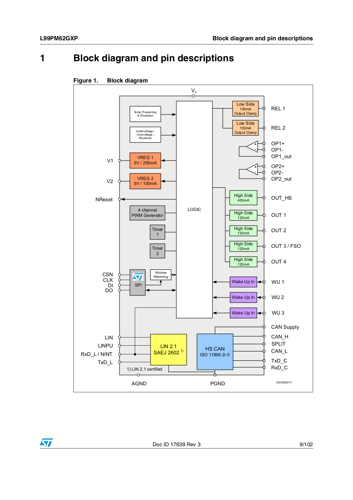
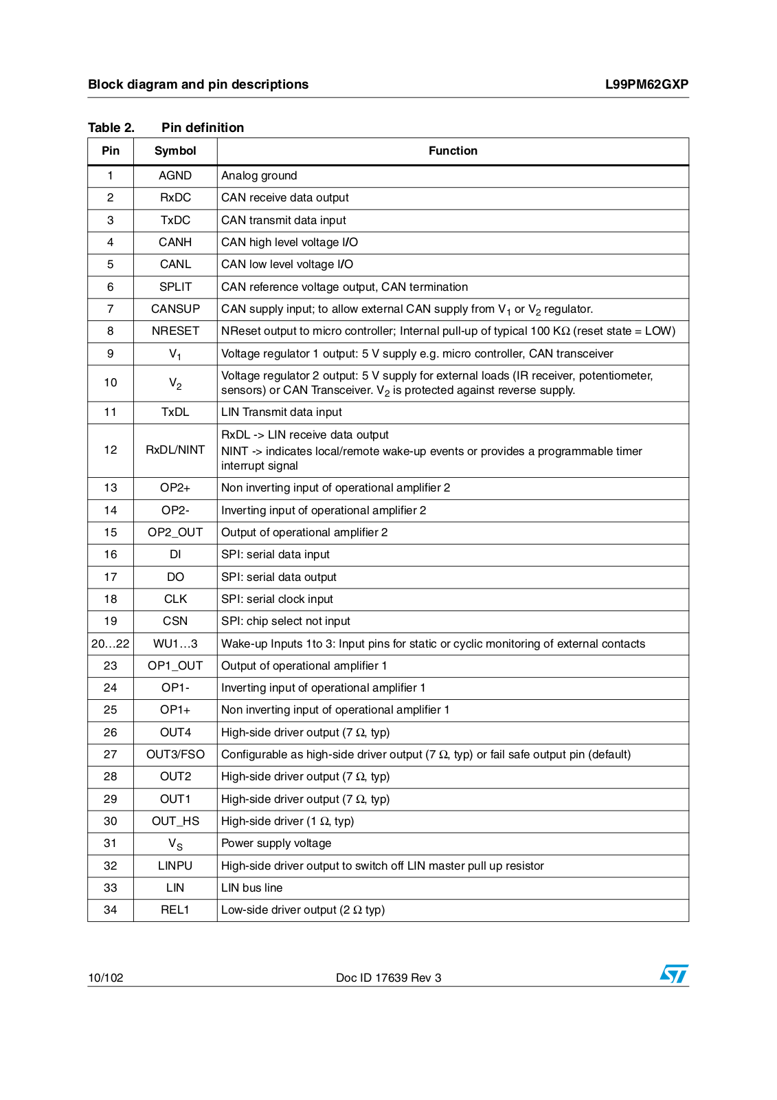
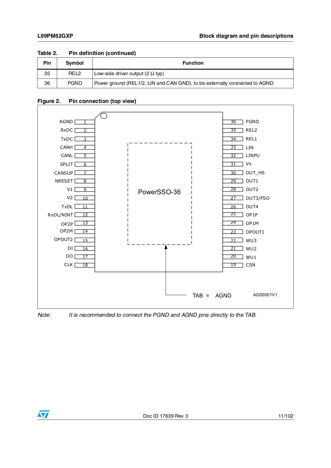
L99PM62GXP
User Manual
102 pgs
1.42 Mb
0
Table of contents
Loading...
ST L99PM62GXP User Manual
...
ST User Manual
Download
Specifications and Main Features
Frequently Asked Questions
User Manual
Download
Loading...
+
hidden pages
Unhide
You need points to download manuals.
1 point = 1 manual.
You can buy points or you can get point for every manual you upload.
Buy points
Upload your manuals
 Loading...