

Page 1
Features
■ 3 independently self configuring high-/low-side
channels
■ 3 low-side channels
■ R
■ Current limit of each output at min. 0.6 A
■ PWM direct mode
■ Bulb mode with recovery mode
■ LED mode with slew rate control
■ Bridge mode with crosscurrent protection
■ SPI interface for data communication
■ Temperature warning
■ All outputs overtemperature protected
■ All outputs short-circuit protected
■ Configurable open-load detection in off mode
■ V
■ Very low current consumption in standby mode
=0.7 Ω (typ) at Tj = 25 °C
ON
supply voltage 3.0 V to 5.25 V
CC
5 µA (typ)
■ Internal clamp diodes
■ HS switches operate down to 3 V crank voltage
Applications
■ Relay driver
■ LED driver
■ Motor driver
■ Mirror adjustment
Table 1. Device summary
L99MC6
Configurable 6-channel device
PowerSSO-16
Description
The L99MC6 IC is a highly flexible monolithic
medium current output driver that incorporates 3
dedicated low-side outputs (channels 4 to 6) and
3 independently self configuring outputs
(channels 1 to 3) that can be used as either lowside or high-side drivers in any combination. The
L99MC6 can control inductive loads,
incandescent bulbs or LEDs.
The L99MC6 can be used in a half bridge
configuration with crosscurrent protection.
The channel 2 can be controlled directly via the
IN/PWM pin for PWM applications. The IN/PWM
signal can be applied to any other output.
The integrated 16-bit standard serial peripheral
interface (SPI) controls all outputs and provides
diagnostic information: normal operation, openload in off-state, overcurrent, temperature
warning, overtemperature.
Order codes
Package
Part number (tube) Part number (tape & reel)
PowerSSO-16 L99MC6-LF L99MC6TR-LF
November 2009 Doc ID 16523 Rev 1 1/55
www.st.com
1
Page 2

Contents L99MC6
Contents
1 Introduction . . . . . . . . . . . . . . . . . . . . . . . . . . . . . . . . . . . . . . . . . . . . . . . . 8
1.1 Application diagram . . . . . . . . . . . . . . . . . . . . . . . . . . . . . . . . . . . . . . . . . . 8
1.2 Block diagram and pin description . . . . . . . . . . . . . . . . . . . . . . . . . . . . . . . 9
2 Description . . . . . . . . . . . . . . . . . . . . . . . . . . . . . . . . . . . . . . . . . . . . . . . . 12
2.1 Dual power supply: VS and V
2.1.1 Channels . . . . . . . . . . . . . . . . . . . . . . . . . . . . . . . . . . . . . . . . . . . . . . . . 12
2.2 Standby mode . . . . . . . . . . . . . . . . . . . . . . . . . . . . . . . . . . . . . . . . . . . . . 13
2.3 Inductive loads . . . . . . . . . . . . . . . . . . . . . . . . . . . . . . . . . . . . . . . . . . . . . 13
2.4 Diagnostic functions . . . . . . . . . . . . . . . . . . . . . . . . . . . . . . . . . . . . . . . . . 13
2.4.1 Direct input IN/PWM . . . . . . . . . . . . . . . . . . . . . . . . . . . . . . . . . . . . . . . 14
2.4.2 Temperature warning and thermal shutdown . . . . . . . . . . . . . . . . . . . . . 14
2.4.3 Open-load detection in off-state . . . . . . . . . . . . . . . . . . . . . . . . . . . . . . . 14
2.4.4 Overload detection . . . . . . . . . . . . . . . . . . . . . . . . . . . . . . . . . . . . . . . . . 14
2.5 Bridge mode . . . . . . . . . . . . . . . . . . . . . . . . . . . . . . . . . . . . . . . . . . . . . . . 14
2.6 LED mode . . . . . . . . . . . . . . . . . . . . . . . . . . . . . . . . . . . . . . . . . . . . . . . . 15
2.7 Bulb mode (programmable soft start function to drive loads with higher
inrush current) . . . . . . . . . . . . . . . . . . . . . . . . . . . . . . . . . . . . . . . . . . . . . 16
. . . . . . . . . . . . . . . . . . . . . . . . . . . . . . . . 12
CC
3 Absolute maximum ratings . . . . . . . . . . . . . . . . . . . . . . . . . . . . . . . . . . 17
4 ESD protection . . . . . . . . . . . . . . . . . . . . . . . . . . . . . . . . . . . . . . . . . . . . 18
5 Thermal data . . . . . . . . . . . . . . . . . . . . . . . . . . . . . . . . . . . . . . . . . . . . . . 19
5.1 Temperature warning and thermal shutdown . . . . . . . . . . . . . . . . . . . . . . 19
6 Electrical characteristics . . . . . . . . . . . . . . . . . . . . . . . . . . . . . . . . . . . . 20
6.1 Supply . . . . . . . . . . . . . . . . . . . . . . . . . . . . . . . . . . . . . . . . . . . . . . . . . . . 20
6.2 Undervoltage detection . . . . . . . . . . . . . . . . . . . . . . . . . . . . . . . . . . . . . . 20
6.3 Channels . . . . . . . . . . . . . . . . . . . . . . . . . . . . . . . . . . . . . . . . . . . . . . . . . 21
7 SPI electrical characteristics . . . . . . . . . . . . . . . . . . . . . . . . . . . . . . . . . 23
7.1 DC characteristics . . . . . . . . . . . . . . . . . . . . . . . . . . . . . . . . . . . . . . . . . . 23
2/55 Doc ID 16523 Rev 1
Page 3

L99MC6 Contents
7.2 AC characteristics . . . . . . . . . . . . . . . . . . . . . . . . . . . . . . . . . . . . . . . . . . 23
7.3 Dynamic characteristics . . . . . . . . . . . . . . . . . . . . . . . . . . . . . . . . . . . . . . 24
7.4 SPI timing parameter definition . . . . . . . . . . . . . . . . . . . . . . . . . . . . . . . . 25
8 Functional description of the SPI . . . . . . . . . . . . . . . . . . . . . . . . . . . . . 27
8.1 Signal description . . . . . . . . . . . . . . . . . . . . . . . . . . . . . . . . . . . . . . . . . . . 27
8.1.1 Serial clock (SCK) . . . . . . . . . . . . . . . . . . . . . . . . . . . . . . . . . . . . . . . . . 27
8.1.2 Serial data input (SDI) . . . . . . . . . . . . . . . . . . . . . . . . . . . . . . . . . . . . . . 27
8.1.3 Serial data output (SDO) . . . . . . . . . . . . . . . . . . . . . . . . . . . . . . . . . . . . 27
8.1.4 Chip select not (CSN) . . . . . . . . . . . . . . . . . . . . . . . . . . . . . . . . . . . . . . 27
8.2 SPI communication flow . . . . . . . . . . . . . . . . . . . . . . . . . . . . . . . . . . . . . . 29
8.2.1 General description . . . . . . . . . . . . . . . . . . . . . . . . . . . . . . . . . . . . . . . . 29
8.2.2 Command byte . . . . . . . . . . . . . . . . . . . . . . . . . . . . . . . . . . . . . . . . . . . 29
8.2.3 Global status register . . . . . . . . . . . . . . . . . . . . . . . . . . . . . . . . . . . . . . . 30
8.3 Write operation . . . . . . . . . . . . . . . . . . . . . . . . . . . . . . . . . . . . . . . . . . . . . 32
8.4 Read operation . . . . . . . . . . . . . . . . . . . . . . . . . . . . . . . . . . . . . . . . . . . . . 32
8.5 Read and Clear Status operation . . . . . . . . . . . . . . . . . . . . . . . . . . . . . . . 33
8.6 Read Device Information . . . . . . . . . . . . . . . . . . . . . . . . . . . . . . . . . . . . . 33
9 SPI control and status register . . . . . . . . . . . . . . . . . . . . . . . . . . . . . . . 34
9.1 RAM memory map . . . . . . . . . . . . . . . . . . . . . . . . . . . . . . . . . . . . . . . . . . 34
9.2 ROM memory map (access with OC0 and OC1 set to ‘1’) . . . . . . . . . . . . 34
9.3 Control and status registers . . . . . . . . . . . . . . . . . . . . . . . . . . . . . . . . . . . 34
9.3.1 Channel configuration decoding . . . . . . . . . . . . . . . . . . . . . . . . . . . . . . 36
9.3.2 Register description . . . . . . . . . . . . . . . . . . . . . . . . . . . . . . . . . . . . . . . . 36
9.4 Examples . . . . . . . . . . . . . . . . . . . . . . . . . . . . . . . . . . . . . . . . . . . . . . . . . 37
9.4.1 Example 1:Switch on channel 1 . . . . . . . . . . . . . . . . . . . . . . . . . . . . . . . 37
9.4.2 Example 2: Bridge mode configuration . . . . . . . . . . . . . . . . . . . . . . . . . 38
9.4.3 Example 3: Open-load detection in off-state in bridge configuration . . . 40
10 Maximum demagnetization energy . . . . . . . . . . . . . . . . . . . . . . . . . . . . 42
11 Application examples . . . . . . . . . . . . . . . . . . . . . . . . . . . . . . . . . . . . . . . 45
12 Package and PCB thermal data . . . . . . . . . . . . . . . . . . . . . . . . . . . . . . . 48
12.1 PowerSSO-16 thermal data . . . . . . . . . . . . . . . . . . . . . . . . . . . . . . . . . . . 48
Doc ID 16523 Rev 1 3/55
Page 4

Contents L99MC6
13 Package and packing information . . . . . . . . . . . . . . . . . . . . . . . . . . . . . 50
13.1 ECOPACK® . . . . . . . . . . . . . . . . . . . . . . . . . . . . . . . . . . . . . . . . . . . . . . . 50
13.2 PowerSSO-16 package information . . . . . . . . . . . . . . . . . . . . . . . . . . . . . 50
13.3 Packing information . . . . . . . . . . . . . . . . . . . . . . . . . . . . . . . . . . . . . . . . . 52
Appendix A Acronyms . . . . . . . . . . . . . . . . . . . . . . . . . . . . . . . . . . . . . . . . . . . . . . 53
Revision history . . . . . . . . . . . . . . . . . . . . . . . . . . . . . . . . . . . . . . . . . . . . . . . . . . . . 54
4/55 Doc ID 16523 Rev 1
Page 5

L99MC6 List of tables
List of tables
Table 1. Device summary . . . . . . . . . . . . . . . . . . . . . . . . . . . . . . . . . . . . . . . . . . . . . . . . . . . . . . . . . . 1
Table 2. Pin functions . . . . . . . . . . . . . . . . . . . . . . . . . . . . . . . . . . . . . . . . . . . . . . . . . . . . . . . . . . . . 10
Table 3. Absolute maximum ratings . . . . . . . . . . . . . . . . . . . . . . . . . . . . . . . . . . . . . . . . . . . . . . . . . 17
Table 4. ESD protection . . . . . . . . . . . . . . . . . . . . . . . . . . . . . . . . . . . . . . . . . . . . . . . . . . . . . . . . . . 18
Table 5. Temperature warning and thermal shutdown . . . . . . . . . . . . . . . . . . . . . . . . . . . . . . . . . . . 19
Table 6. Supply . . . . . . . . . . . . . . . . . . . . . . . . . . . . . . . . . . . . . . . . . . . . . . . . . . . . . . . . . . . . . . . . . 20
Table 7. Undervoltage detection . . . . . . . . . . . . . . . . . . . . . . . . . . . . . . . . . . . . . . . . . . . . . . . . . . . . 20
Table 8. Channels. . . . . . . . . . . . . . . . . . . . . . . . . . . . . . . . . . . . . . . . . . . . . . . . . . . . . . . . . . . . . . . 21
Table 9. DC characteristics. . . . . . . . . . . . . . . . . . . . . . . . . . . . . . . . . . . . . . . . . . . . . . . . . . . . . . . . 23
Table 10. AC characteristics . . . . . . . . . . . . . . . . . . . . . . . . . . . . . . . . . . . . . . . . . . . . . . . . . . . . . . . . 23
Table 11. Dynamic characteristic . . . . . . . . . . . . . . . . . . . . . . . . . . . . . . . . . . . . . . . . . . . . . . . . . . . . 24
Table 12. Command byte - general description . . . . . . . . . . . . . . . . . . . . . . . . . . . . . . . . . . . . . . . . . 29
Table 13. Data byte - general description . . . . . . . . . . . . . . . . . . . . . . . . . . . . . . . . . . . . . . . . . . . . . . 29
Table 14. Command byte . . . . . . . . . . . . . . . . . . . . . . . . . . . . . . . . . . . . . . . . . . . . . . . . . . . . . . . . . . 29
Table 15. Operating code definition . . . . . . . . . . . . . . . . . . . . . . . . . . . . . . . . . . . . . . . . . . . . . . . . . . 30
Table 16. Global status register . . . . . . . . . . . . . . . . . . . . . . . . . . . . . . . . . . . . . . . . . . . . . . . . . . . . . 30
Table 17. Global status register description . . . . . . . . . . . . . . . . . . . . . . . . . . . . . . . . . . . . . . . . . . . . 30
Table 18. Command byte for Write mode . . . . . . . . . . . . . . . . . . . . . . . . . . . . . . . . . . . . . . . . . . . . . . 32
Table 19. Command byte for Read mode. . . . . . . . . . . . . . . . . . . . . . . . . . . . . . . . . . . . . . . . . . . . . . 32
Table 20. Command byte for Read and Clear Status operation . . . . . . . . . . . . . . . . . . . . . . . . . . . . . 33
Table 21. Command byte for Read Device Information . . . . . . . . . . . . . . . . . . . . . . . . . . . . . . . . . . . 33
Table 22. RAM memory map . . . . . . . . . . . . . . . . . . . . . . . . . . . . . . . . . . . . . . . . . . . . . . . . . . . . . . . 34
Table 23. ROM memory map . . . . . . . . . . . . . . . . . . . . . . . . . . . . . . . . . . . . . . . . . . . . . . . . . . . . . . . 34
Table 24. Control register 0 . . . . . . . . . . . . . . . . . . . . . . . . . . . . . . . . . . . . . . . . . . . . . . . . . . . . . . . . 34
Table 25. Control register 1 . . . . . . . . . . . . . . . . . . . . . . . . . . . . . . . . . . . . . . . . . . . . . . . . . . . . . . . . 35
Table 26. Control register 2 . . . . . . . . . . . . . . . . . . . . . . . . . . . . . . . . . . . . . . . . . . . . . . . . . . . . . . . . 35
Table 27. Status register 0 . . . . . . . . . . . . . . . . . . . . . . . . . . . . . . . . . . . . . . . . . . . . . . . . . . . . . . . . . 35
Table 28. Status register 1 . . . . . . . . . . . . . . . . . . . . . . . . . . . . . . . . . . . . . . . . . . . . . . . . . . . . . . . . . 35
Table 29. Channel configuration decoding . . . . . . . . . . . . . . . . . . . . . . . . . . . . . . . . . . . . . . . . . . . . . 36
Table 30. Register description . . . . . . . . . . . . . . . . . . . . . . . . . . . . . . . . . . . . . . . . . . . . . . . . . . . . . . 36
Table 31. Command byte - example 1 . . . . . . . . . . . . . . . . . . . . . . . . . . . . . . . . . . . . . . . . . . . . . . . . 37
Table 32. Data byte - example 1. . . . . . . . . . . . . . . . . . . . . . . . . . . . . . . . . . . . . . . . . . . . . . . . . . . . . 37
Table 33. Data byte description - example 1 . . . . . . . . . . . . . . . . . . . . . . . . . . . . . . . . . . . . . . . . . . . 37
Table 34. Command byte 1 - example 2 . . . . . . . . . . . . . . . . . . . . . . . . . . . . . . . . . . . . . . . . . . . . . . . 38
Table 35. Data byte 1 - example 2 . . . . . . . . . . . . . . . . . . . . . . . . . . . . . . . . . . . . . . . . . . . . . . . . . . . 38
Table 36. Data byte description 1 - example 2 . . . . . . . . . . . . . . . . . . . . . . . . . . . . . . . . . . . . . . . . . . 38
Table 37. Command byte 2 - example 2 . . . . . . . . . . . . . . . . . . . . . . . . . . . . . . . . . . . . . . . . . . . . . . . 38
Table 38. Data byte 2 - example 2 . . . . . . . . . . . . . . . . . . . . . . . . . . . . . . . . . . . . . . . . . . . . . . . . . . . 38
Table 39. Data byte description 2 - example 2 . . . . . . . . . . . . . . . . . . . . . . . . . . . . . . . . . . . . . . . . . . 39
Table 40. Command byte 1 - example 3 . . . . . . . . . . . . . . . . . . . . . . . . . . . . . . . . . . . . . . . . . . . . . . . 40
Table 41. Data byte 1 - example 3 . . . . . . . . . . . . . . . . . . . . . . . . . . . . . . . . . . . . . . . . . . . . . . . . . . . 40
Table 42. Data byte description 1 - example 3 . . . . . . . . . . . . . . . . . . . . . . . . . . . . . . . . . . . . . . . . . . 40
Table 43. Command byte 2 - example 3 . . . . . . . . . . . . . . . . . . . . . . . . . . . . . . . . . . . . . . . . . . . . . . . 40
Table 44. Data byte 2 - example 3 . . . . . . . . . . . . . . . . . . . . . . . . . . . . . . . . . . . . . . . . . . . . . . . . . . . 40
Table 45. Data byte description 2 - example 3 . . . . . . . . . . . . . . . . . . . . . . . . . . . . . . . . . . . . . . . . . . 41
Table 46. Auto and mutual thermal resistance - footprint . . . . . . . . . . . . . . . . . . . . . . . . . . . . . . . . . . 48
Table 47. Auto and mutual thermal resistance - 2 cm
Table 48. Auto and mutual thermal resistance - 8 cm
2
of Cu heatsink. . . . . . . . . . . . . . . . . . . . . . . . 48
2
of Cu heatsink. . . . . . . . . . . . . . . . . . . . . . . . 49
Doc ID 16523 Rev 1 5/55
Page 6

List of tables L99MC6
Table 49. PowerSSO-16 mechanical data . . . . . . . . . . . . . . . . . . . . . . . . . . . . . . . . . . . . . . . . . . . . . 51
Table 50. Acronyms . . . . . . . . . . . . . . . . . . . . . . . . . . . . . . . . . . . . . . . . . . . . . . . . . . . . . . . . . . . . . . 53
Table 51. Document revision history . . . . . . . . . . . . . . . . . . . . . . . . . . . . . . . . . . . . . . . . . . . . . . . . . 54
6/55 Doc ID 16523 Rev 1
Page 7

L99MC6 List of figures
List of figures
Figure 1. Application diagram . . . . . . . . . . . . . . . . . . . . . . . . . . . . . . . . . . . . . . . . . . . . . . . . . . . . . . . 8
Figure 2. Block diagram . . . . . . . . . . . . . . . . . . . . . . . . . . . . . . . . . . . . . . . . . . . . . . . . . . . . . . . . . . . . 9
Figure 3. Configuration diagram (top view) not in scale. . . . . . . . . . . . . . . . . . . . . . . . . . . . . . . . . . . 11
Figure 4. Power-on reset . . . . . . . . . . . . . . . . . . . . . . . . . . . . . . . . . . . . . . . . . . . . . . . . . . . . . . . . . . 12
Figure 5. Output voltage clamping . . . . . . . . . . . . . . . . . . . . . . . . . . . . . . . . . . . . . . . . . . . . . . . . . . . 13
Figure 6. Example of bridge configuration . . . . . . . . . . . . . . . . . . . . . . . . . . . . . . . . . . . . . . . . . . . . . 15
Figure 7. Example of programmable soft start function for inductive loads and incandescent bulbs. 16
Figure 8. Serial input timing . . . . . . . . . . . . . . . . . . . . . . . . . . . . . . . . . . . . . . . . . . . . . . . . . . . . . . . . 25
Figure 9. Serial input timing . . . . . . . . . . . . . . . . . . . . . . . . . . . . . . . . . . . . . . . . . . . . . . . . . . . . . . . . 25
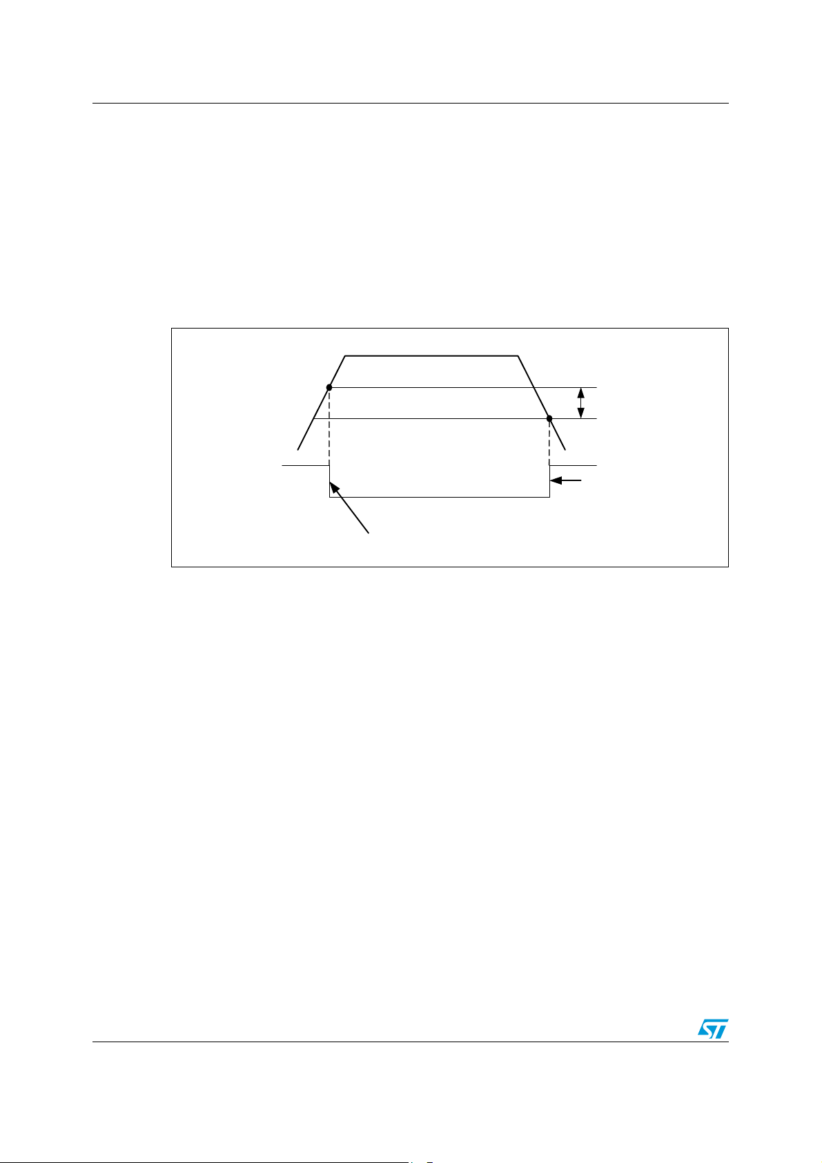
Figure 10. Output turn on/off delays and slew rates . . . . . . . . . . . . . . . . . . . . . . . . . . . . . . . . . . . . . . 26
Figure 11. Clock polarity and clock phase . . . . . . . . . . . . . . . . . . . . . . . . . . . . . . . . . . . . . . . . . . . . . . 27
Figure 12. SPI frame structure . . . . . . . . . . . . . . . . . . . . . . . . . . . . . . . . . . . . . . . . . . . . . . . . . . . . . . . 28
Figure 13. Indication of the global error flag on DO when CSN is low and SCK is stable . . . . . . . . . . 31
Figure 14. Bridge mode drawing . . . . . . . . . . . . . . . . . . . . . . . . . . . . . . . . . . . . . . . . . . . . . . . . . . . . . 39
Figure 15. Open-load in bridge mode drawing. . . . . . . . . . . . . . . . . . . . . . . . . . . . . . . . . . . . . . . . . . . 41
Figure 16. Configurable switch HSD - maximum turn-off current versus inductance. . . . . . . . . . . . . . 42
Figure 17. Configurable switch LSD - maximum turn-off current versus inductance . . . . . . . . . . . . . . 43
Figure 18. Fixed LSD switch - maximum turn-off current versus inductance. . . . . . . . . . . . . . . . . . . . 44
Figure 19. L99MC6 as driver for incandescent bulb, LEDs and high-side or low-side relays . . . . . . . 45
Figure 20. L99MC6 as motor driver (for example, for mirror adjustment) . . . . . . . . . . . . . . . . . . . . . . 46
Figure 21. L99MC6 as driver for unipolar stepper motor driver, relay and LEDs . . . . . . . . . . . . . . . . . 47
Figure 22. PowerSSO-16 PC board
Figure 23. PowerSSO-16 package dimensions . . . . . . . . . . . . . . . . . . . . . . . . . . . . . . . . . . . . . . . . . . 50
Figure 24. PowerSSO-16 tube shipment (no suffix) . . . . . . . . . . . . . . . . . . . . . . . . . . . . . . . . . . . . . . 52
Figure 25. PowerSSO-16 tape and reel shipment (suffix “TR”) . . . . . . . . . . . . . . . . . . . . . . . . . . . . . . 52
(1)
. . . . . . . . . . . . . . . . . . . . . . . . . . . . . . . . . . . . . . . . . . . . . . . . . 48
Doc ID 16523 Rev 1 7/55
Page 8
Introduction L99MC6
1 Introduction
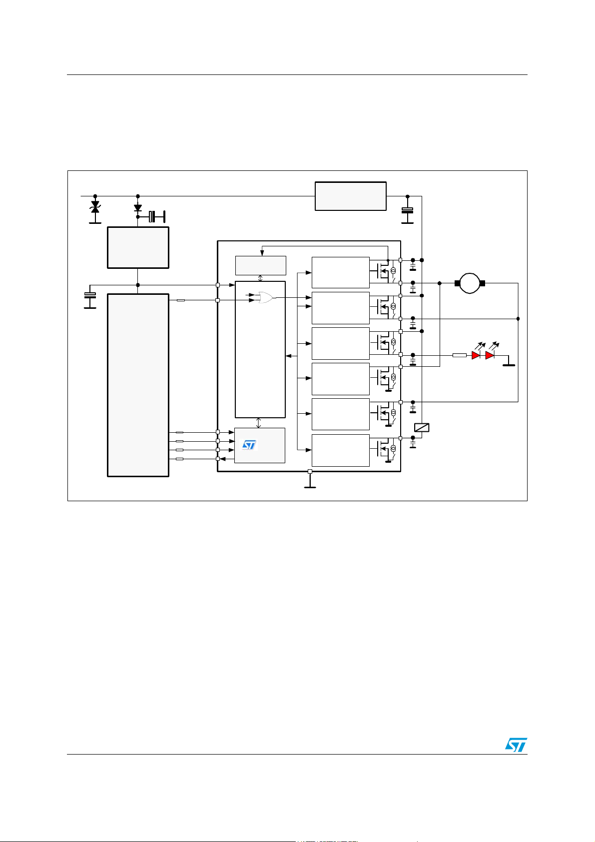
1.1 Application diagram
Figure 1. Application diagram
V
Bat
VREG
Charge
Pump
Vcc
PWM / IN
Active reverse
polarity protection
Dri ver and
Protections
Config. OUT1
Dri ver and
Protections
Config. OUT2
OL
M
OL
Microcontroller
CSN
SCK
DI
DO
CONTROL
LOGIC
SPI
GND
Dri ver and
Protections
Config. OUT3
Dri ver and
Protections
LSD OUT4
Dri ver and
Protections
LSD OUT5
Driver and
Protections
LSD OUT6
OL
OL
OL
OL
8/55 Doc ID 16523 Rev 1
Page 9
L99MC6 Introduction
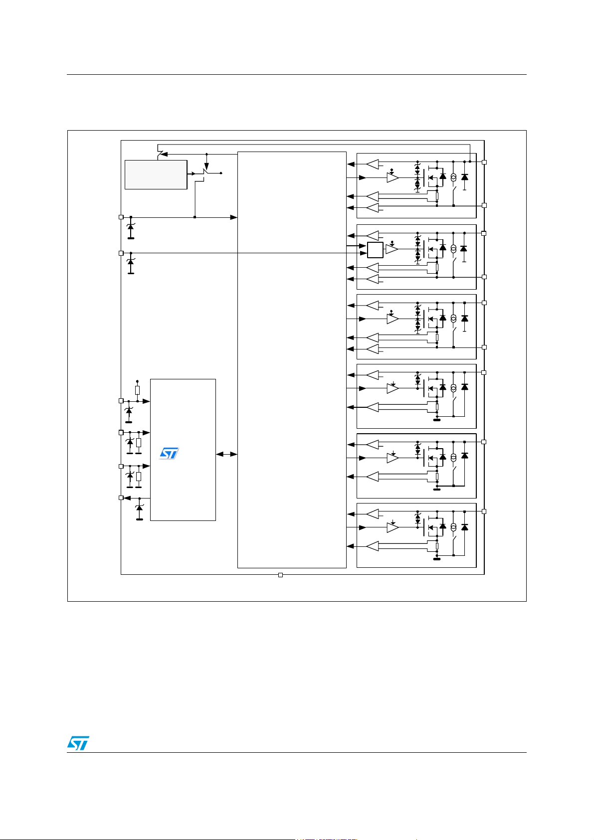
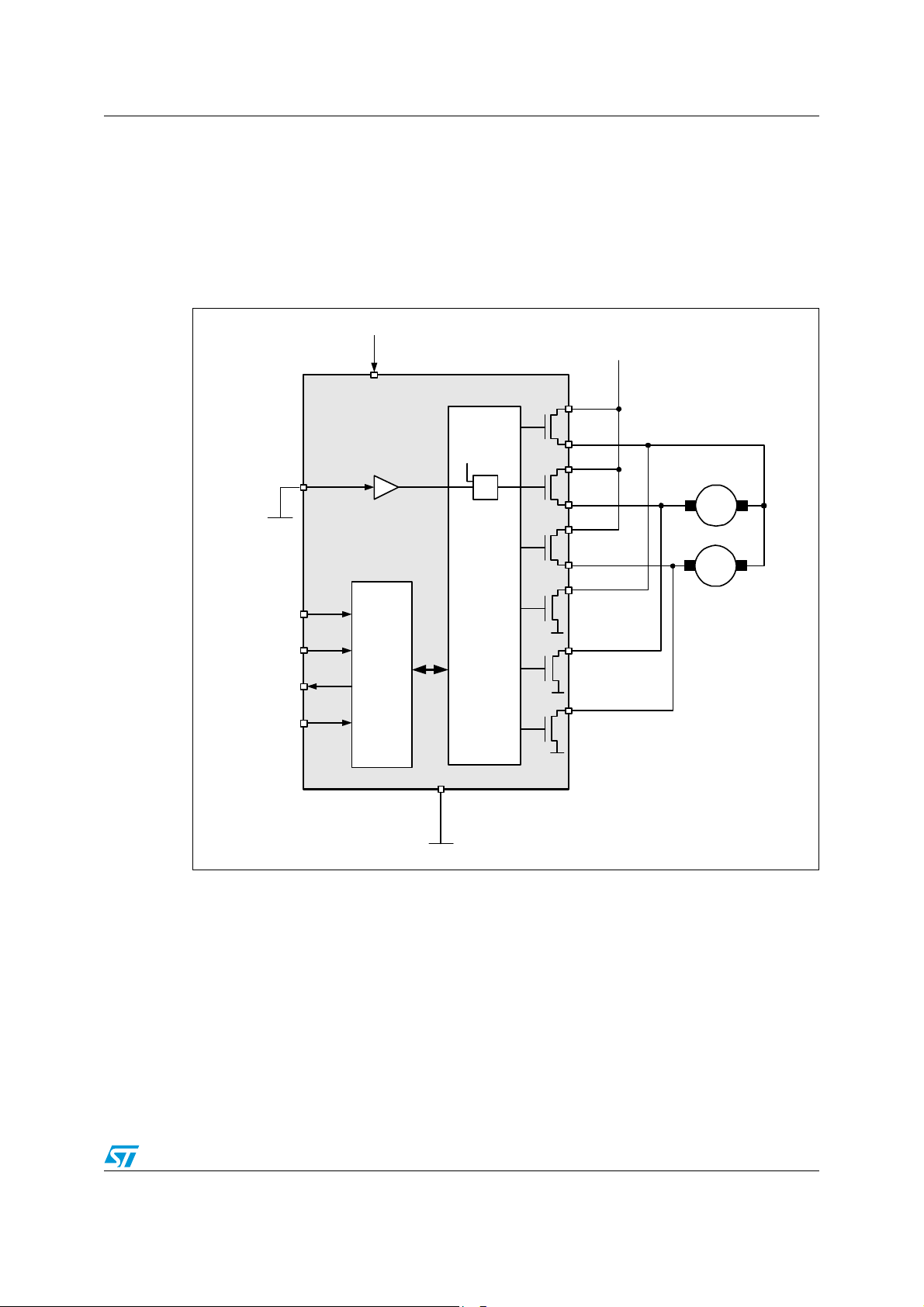
1.2 Block diagram and pin description
Figure 2. Block diagram
VCC
IN/PWM
CSN
SCK
DI
DO
Charge
Pump
VCC
SPI
VCP
VDr ive1-3
Open Load Drain [Out1]
ON/OF F [ Out1]
Short Circuit [Out1]
Open Load Source [Out1]
Open Load Drain [Out2]
ON/OF F [ Out2]
Short Circuit [Out2]
Open Load Source [Out2]
Open Load Drain [Out3]
ON/OF F [ Out3]
Short Circuit [Out3]
Open Load Source [Out3]
CONTROL LOGIC
Open Load Drain [Out4]
ON/OF F [ Out4]
Short Circuit [Out4]
Open Load Drain [Out5]
ON/OF F [ Out5]
Short Circuit [Out5]
Open Load Drain [Out6]
ON/OF F [ Out6]
VOLD 1
VOLS 1
VOLD 2
VDr ive1-3
VDr ive1-3
OL
OL
DRN1
SRC1
DRN2
=1
VOLS2
VOLD 3
VOLS 3
VOLD 4
VOLD 5
VDr ive1-3
VCC
VCC
OL
OL
OL
SRC2
DRN3
SRC3
DRN4
DRN5
0
VOLD 6
VCC
OL
DRN6
Short Circuit [Out6]
GND
Doc ID 16523 Rev 1 9/55
Page 10

Introduction L99MC6
Table 2. Pin functions
Pin Symbol Function
1 / TAB GND
6IN/PWM
8VCC
3 SRC1 Source of configurable channel 1
4 DRN1 Drain of self configurable channel 1, in HS mode also V
5 DRN2 Drain of self configurable channel 2
15 SRC2 Source of self configurable channel 2
12 DRN3 Drain of self configurable channel 3
13 SRC3 Source of self configurable channel 3
2 DRN4 Drain of channel 4
16 DRN5 Drain of channel 5
14 DRN6 Drain of channel 6
11 DI
Ground:
Reference potential
IN/PWM direct mode:
Direct input for channel 2. Other channels can be driven in PWM mode via SPI.
Logic voltage supply 3.3 V/5 V:
For this input a ceramic capacitor as close as possible to GND is recommended
supply
S
SPI data in:
The input requires CMOS logic levels and receives serial data from the
microcontroller. The data is a 16-bit control word and the most significant bit
(MSB, bit 7) is transferred first.
SPI data out:
9DO
The diagnosis data is available via the SPI and this tristate-output. The output
remains in tristate, if the chip is not selected by the input CSN (CSN = high).
SPI chip select not (active low):
7CSN
This input is low active and requires CMOS logic levels. The serial data transfer
between the L99MC6 and microcontroller is enabled by pulling the input CSN to
low-level.
SPI serial clock input:
10 SCK
This input controls the internal shift register of the SPI and requires CMOS logic
levels.
10/55 Doc ID 16523 Rev 1
Page 11
L99MC6 Introduction
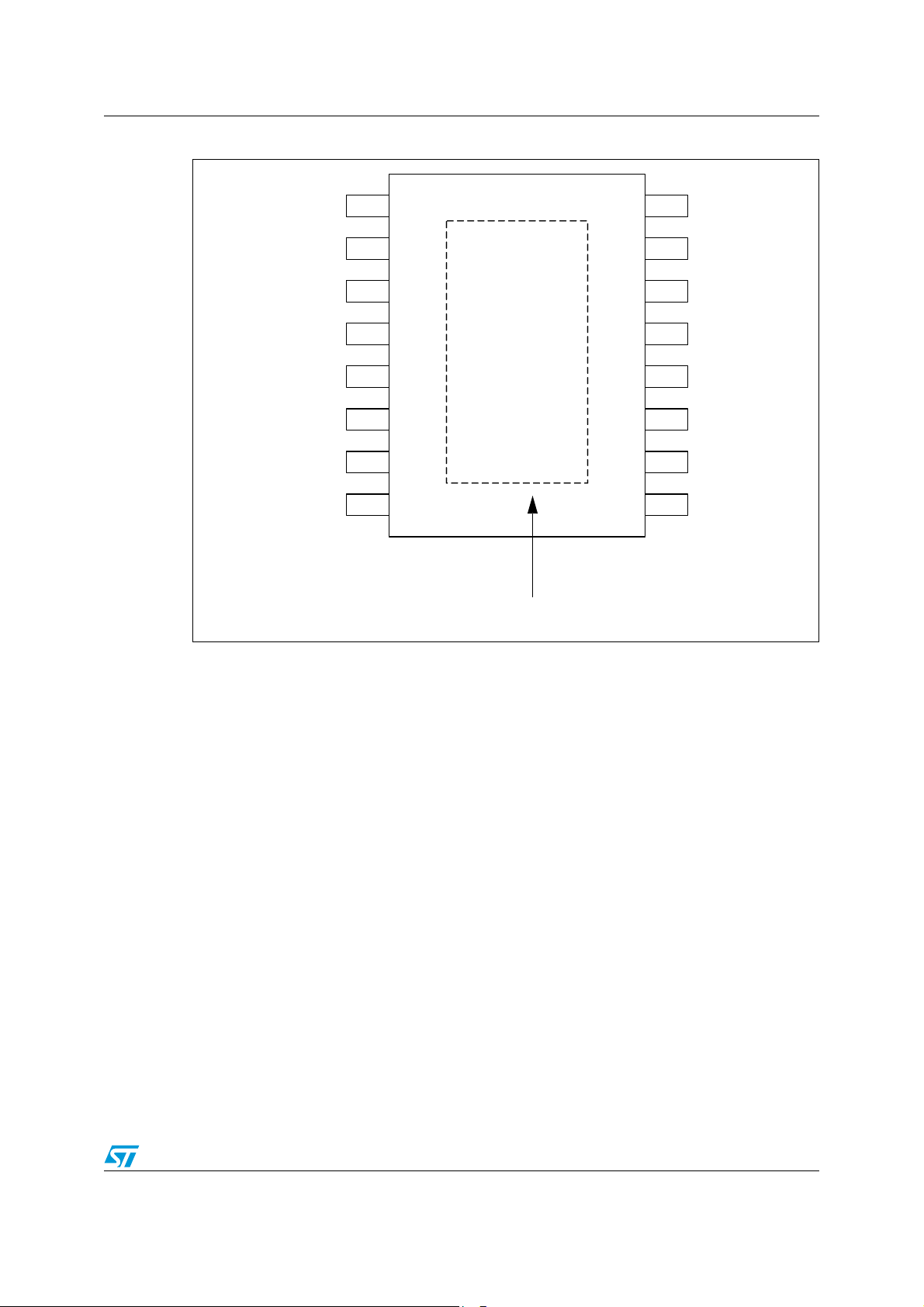
Figure 3. Configuration diagram (top view) not in scale
GND
1
16
DRN5
DRN4
SRC1
DRN1
DRN2
PWM/IN
CSN
VCC
The tab must be connected to GND
2
3
4
PowerSSO-16
5
6
7
8
TAB = GN D
15
14
13
12
11
8
9
SRC2
DRN6
SRC3
DRN3
DI
SCK
DO
Doc ID 16523 Rev 1 11/55
Page 12
Description L99MC6
2 Description
2.1 Dual power supply: VS and V
The supply voltage VCC (3.3 V/5 V) supplies the whole device. In case of power-on (VCC
increases from undervoltage to V
internally generated power-on reset (POR). If the voltage V
minimum threshold (V
POR ON
impedance) and the status registers are cleared (see Figure 4).
Figure 4. Power-on reset
V
V
POR OFF
V
POR ON
All Status Registers are cleared
POR OFF
= 2.4 V, typical), the outputs are switched-off (high-
CC
CC
= 2.7 V, typical) the circuit is initialized by an
decreases under the
CC
V
POR hyst.
IC is disabled
2.1.1 Channels
The channels 1 to 3 are self configuring high-side or low-side n-channel mosfets. This
flexibility allows the user to connect loads in high-side or low-side configuration in any
combination.
In order to provide low R
charge pump (CP) to drive the internal gate voltage(s) is implemented. If the charge pump is
activated (ENCP1 = 1, DISCP2 = 0, see Section 9.3: Control and status registers), the
internal charge-pump uses V
V
is used to drive all channels.
CC
The channels 4 to 6 are n-channel low-side drivers. The source of the respective mosfet are
internally connected to the device GND.
Caution: For any high-side configuration, channel 1 must be used as a high-side switch.
If channel 1 is configured as low-side, the charge pump has to be deactivated to avoid
charge pump current from the drain.
Caution: The charge pump may not be deactivated (see Section 9.3: Control and status registers) if
one of the channels is in high-side configuration, while a short-circuit from the source to the
battery is present. If these conditions occur, the voltage of the shorted source is applied to
the VCC pin.
values for high-side configured switches (channels 1 to 3), a
dson
from the drain of channel 1, as its power source. Otherwise
S
12/55 Doc ID 16523 Rev 1
Page 13
L99MC6 Description
2.2 Standby mode
The standby mode of the L99MC6 is activated by SPI command (EN bit of CTRL 0 reset to
0, see Section 9.3.2: Register description). The inputs and outputs are switched-off. The
status registers are cleared and the control registers are reset to their default values.
In the standby mode the current consumption is 5 µA (typical value). A SPI command is
needed to switch the L99MC6 in normal mode.
2.3 Inductive loads
Each switch is built by a power DMOS transistor. For low-side configured outputs an internal
zener clamp from the drain to gate with a breakdown of 31 V minimum provides for fast turnoff of inductive loads.
For high-side configured outputs, an internal zener clamp with a breakdown of -15 V
maximum provides for fast turn-off of inductive loads (Figure 5).
The maximum clamping energy is specified in Chapter 10.
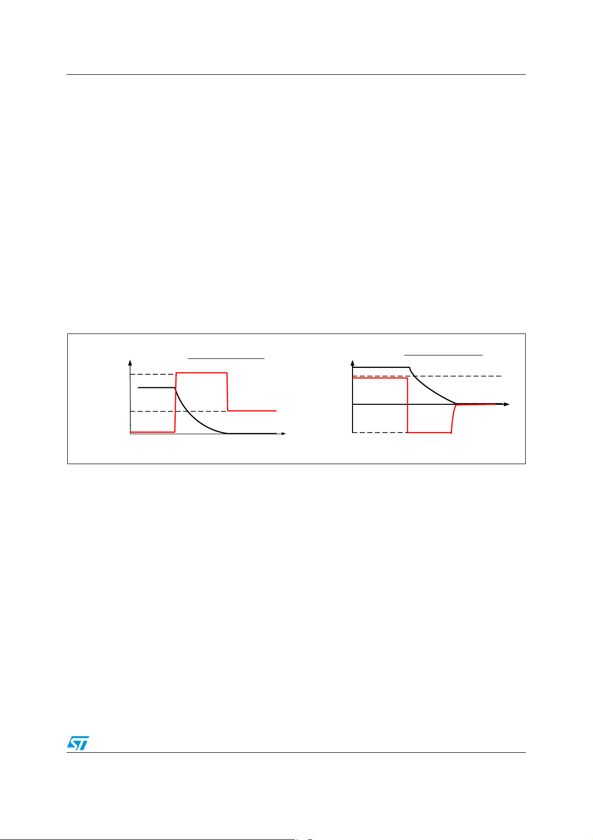
Figure 5. Output voltage clamping
Low Side Configuration
Drain Clamp
Voltage
(V
DRN_CL1-6)
= 35V)
V
GND
Output Current
S
Drain Voltage
2.4 Diagnostic functions
All diagnostic functions (overload, open-load, temperature warning and thermal shutdown)
are internally filtered and the condition has to be valid for at least 32 µs (open-load: typ.
400 µs, respectively) before the corresponding status bit in the status registers are set. The
filters are used to improve the noise immunity of the device. Open-load and temperature
warning function are intended for information purpose and do not change the state of the
output drivers. On contrary, the overload and thermal shutdown condition disable the
corresponding driver (overload) or all drivers (thermal shutdown), respectively. Without
setting the overcurrent recovery bit in the input data register to logic high, the microcontroller
has to clear the overcurrent status bit to reactivate the corresponding driver. (All switches
have a corresponding overcurrent recovery bit) If this bit is set, the device automatically
switches-on the outputs again after a short recovery time. With this feature the device can
drive loads with start-up currents higher than the overcurrent limits (that is inrush current of
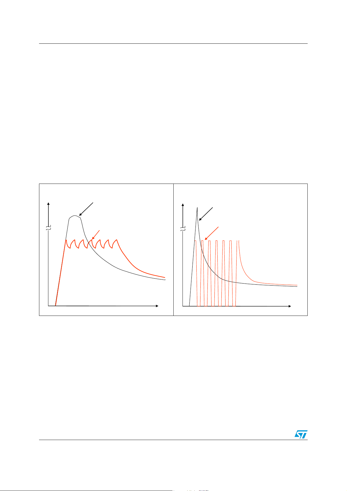
incandescent lamps, cold resistance of motors and heaters, Figure 7).
Time
GND
Source Clamp
Voltage
(V
SRC_CL1-3)
= -19V)
High Side Configuration
Output Current
V
S
Time
Source Voltage
Doc ID 16523 Rev 1 13/55
Page 14

Description L99MC6
2.4.1 Direct input IN/PWM
The IN/PWM input allows channel 2 to be enabled without the use of SPI. The IN/PWM pin
is OR-ed with the SPI command bit. This pin can be left open if the channel 2 is controlled
only via the SPI. This input has an internal pull-down.
The IN/PWM signal can also be applied to any other switches by the activation of the PWM
mode.
This input is suited for non-inductive loads that are pulse width modulated. This allows PWM
control without further use of the SPI.
2.4.2 Temperature warning and thermal shutdown
If the junction temperature rises above T
detectable via the SPI. If the junction temperature increases above the second threshold
T
, the thermal shutdown bit is set and power DMOS transistors of all output stages are
jSD
switched-off to protect the device. Temperature warning flag and thermal shutdown bits are
latched. In order to reactivate the output stages, the junction temperature must decrease
below T
jSD-TjSDHYS
and the thermal shutdown bit has to be cleared by the
microcontroller.
2.4.3 Open-load detection in off-state
The open-load detection monitors the load at each output stage in off mode. A current
source of 150 µA (I
OLD1-6
, I
OLS 1-3
) is connected between drain and source or GND. An
open-load failure is detected if the drain or source voltage reaches an internal V
for at least 3 ms (t
). The corresponding open-load bit is set in the status register. In
dOL typ.
LED mode the open-load detection is disabled and the current source is switched-off, which
avoids a turn-on of the LEDs in off-state.
2.4.4 Overload detection
In case of an overcurrent condition, a flag is set in the corresponding status register. If the
overcurrent signal is valid for at least t
corresponding driver is switched-off to reduce the power dissipation and to protect the
integrated circuit. If the overcurrent recovery bit of the output is zero the microcontroller has
to clear the status bit to reactivate the corresponding driver.
ISC
a temperature warning flag is set and is
j TW
OLD/S
= 32 µs, the overcurrent flag is set and the
(2.0 V)
2.5 Bridge mode
The L99MC6 can be configured as bridge driver. Up to three half bridges can be used. In
Bridge mode the device is crosscurrent protected by an internal delay time. If one driver (LS
or HS) is turned-off the activation of the other driver of the same half bridge is automatically
delayed by the crosscurrent protection time. After the crosscurrent protection time is expired
the slew rate limited switch-off phase of the driver is changed to a fast turn-off phase and the
opposite driver is turned-on with slew-rate limitation. Due to this behavior it is always
guaranteed that the previously activated driver is totally turned-off before the opposite driver
starts to conduct.
Due to the built-in reverse diodes of the output transistors, inductive loads can be driven at
the outputs without external free-wheeling diodes.
14/55 Doc ID 16523 Rev 1
Page 15
L99MC6 Description
The following combination must be used: channel 1 + 4, channel 2 + 5, channel 3 + 6
(Figure 6).
A V
voltage exceeding the low-side clamping voltage (V
S
DRN_CL1-6
) , while the high one of
the high-side drivers is turned on, may cause a destruction of the device.
Caution: In bridge mode using channels 2 and 5, the IN/PWM pin has to be grounded. Therefore
PWM mode on other channels is not possible.
Figure 6. Example of bridge configuration
V
5V
DD
Out1
VS12V
IN/PWM
GND
SCK
CSN
DO
DI
SPI
GND
=1
Control
Out2
M
Out3
M
Out4
Out5
Out6
2.6 LED mode
Open-load detection in off-state can be deactivated to avoid the turn on of the LEDs by the
current source (150 µA typ.) when the channel is switched-off.
Moreover, it is possible to select a high slew rate to support PWM operations with small duty
cycle (see Section 9.3.1: Channel configuration decoding).
Doc ID 16523 Rev 1 15/55
Page 16
Description L99MC6
2.7 Bulb mode (programmable soft start function to drive loads with higher inrush current)
Loads with start-up currents higher than the overcurrent limits (for example inrush current of
lamps, start current of motors and cold resistance of heaters) can be driven by using the
programmable soft start function (that is overcurrent recovery mode). Each driver has a
corresponding overcurrent recovery bit. If this bit is set, the device automatically switches-on
the outputs again after a fixed recovery time. The PWM modulated current provides
sufficient average current to power up the load (for example heat up the bulb) until the load
reaches operating condition (Figure 6).
The device itself cannot distinguish between a real overload and a non linear load like a light
bulb. A real overload condition can only be qualified by time. As an example the
microcontroller can switch-on light bulbs by setting the overcurrent recovery bit for the first
50 ms. After clearing the recovery bit, the output is automatically disabled if the overload
condition still exits.
Figure 7. Example of programmable soft start function for inductive loads and incandescent
Load Current
bulbs
Unlimited Inrush Current
Load Current
Unlimited Inrush Current
Limited Inrush Current in
overcurrent recovery
mode with inductive load
t
Limited Inrush Current in
overcurrent recovery mode
with incandescent bulb
t
16/55 Doc ID 16523 Rev 1
Page 17
L99MC6 Absolute maximum ratings
3 Absolute maximum ratings
Stressing the device above the rating listed in Ta bl e 3 may cause permanent damage to the
device. These are stress ratings only and operation of the device at these or any other
conditions above those indicated in the operating sections of this specification is not implied.
Exposure to absolute maximum rating conditions for extended periods may affect device
reliability. Refer also to the STMicroelectronics™ SURE program and other relevant quality
document.
Table 3. Absolute maximum ratings
Symbol Parameter Value Unit
DC supply voltage -0.3 to 28 V
VS (DRN1 HS
config)
V
CC
DI, DO, SCK,
CSN, IN
Single pulse t
configuration with R
Single pulse t
Stabilized supply voltage, logic supply -0.3 to 5.5 V
Digital input/output voltage -0.3 to VCC + 0.3 V
< 400 ms in HS or LS
max
< 400 ms in bridge mode V
max
load min
= 40 Ω
(1)
40 V
DRN_CL1-6
V
DRN 1-6 Output current capability ±1,65 A
SRC 1-3 Output current capability ±1,65 A
GND Current capability 3,30 A
T
j
1. The device requires a minimum load impedance of 40 Ω to sustain a load dump pulse of 40 V according to
the ISO 7637 pulse 5b.
Operating junction temperature -40 to 150 °C
All maximum ratings are absolute ratings. Leaving the limitation of any of these values may
cause an irreversible damage of the integrated circuit.
Doc ID 16523 Rev 1 17/55
Page 18

ESD protection L99MC6
4 ESD protection
Table 4. ESD protection
Parameter Value Unit
All pins ±2
Output pins: DRN1 – DRN6; SRC1, SRC3, SRC5 ±4
(1)
(2)
Machine model (CDF-AEC-Q100-03 rev. F) ±200 V
Charged device model (CDF-AEC-Q100-011 Rev. F) ±1500 V
1. HBM according to MIL 883C, Method 3015.7 or EIA/JESD22-A114-A
2. HBM with all unzapped pins grounded
kV
kV
18/55 Doc ID 16523 Rev 1
Page 19

L99MC6 Thermal data
5 Thermal data
5.1 Temperature warning and thermal shutdown
Table 5. Temperature warning and thermal shutdown
Item Symbol Parameter Min. Typ. Max. Unit
5.2.1 T
5.2.2 T
5.2.3 T
5.2.4 T
5.2.5 T
5.2.6 T
jTW ON
jTW OFF
jTW HYS
jSD ON
jSD OFF
jSD HYS
Temperature warning threshold
junction temperature
Temperature warning threshold
junction temperature
increasing 150 °C
T
j
decreasing 130 °C
T
j
Temperature warning hysteresis - 5 K
Thermal shutdown threshold
junction temperature
Thermal shutdown threshold
junction temperature
increasing 170 °C
T
j
decreasing 150 °C
T
j
Thermal shutdown hysteresis - 5 K
For additional information, please refer to Chapter 12: Package and PCB thermal data.
Doc ID 16523 Rev 1 19/55
Page 20

Electrical characteristics L99MC6
6 Electrical characteristics
VS=6V to16V,VCC= 3.0 V to 5.3 V, Tj= -40 °C to 150 °C, unless otherwise specified.
The voltages are referred to GND and currents are assumed positive, when the current
flows into the pin.
6.1 Supply
Table 6. Supply
Item Symbol Parameter Test condition Min. Typ. Max. Unit
6.1.1 V
6.1.2 I
Operating supply voltage
S
range
VS DC supply current
S
V
=13V, VCC=5.0V
S
active mode
DRN1 = V
S
628V
1.5 2.0 mA
Outputs floating
=13V, VCC=5V
V
S
standby mode
6.1.3 I
VS
VS quiescent supply current
DRN1 = V
T
= -40 °C, 25 °C
Te st
S
310μA
Outputs floating
T
=130 °C 6 20 μA
Te st
6.1.4 V
6.1.5
6.1.6
I
CC
CC
Operating supply voltage
range
VCC DC supply current
quiescent supply
V
CC
current
VS=13V, VCC=5.0V
active mode
=13V, VCC=5.0V
V
S
CSN = V
CC
standby mode
3.0 5.3 V
1.3 2 mA
520µA
Outputs floating
6.2 Undervoltage detection
Table 7. Undervoltage detection
Item Symbol Parameter Test Condition Min. Typ. Max. Unit
6.2.1
6.2.2
6.2.3
20/55 Doc ID 16523 Rev 1
V
POR OFF
V
POR ON
V
POR hyst
Power-on reset threshold VCC increasing
Power-on reset threshold VCC decreasing
Power-on reset hysteresis V
POR OFF
- V
POR ON
3.0 V
2.2 V
0.3 V
Page 21

L99MC6 Electrical characteristics
6.3 Channels
Table 8. Channels
Item Symbol Parameter Test condition Min. Typ. Max. Unit
=13.5 V, Tj=25°C,
V
6.3.1 r
6.3.2 r
ON SWI1-3
ON SWI1-6
On resistance drain to
source in HS configuration
On resistance drain to
source or GND,
in LS configuration
S
CP on, I
V
=13.5 V, Tj=125°C,
S
CP on, I
=6.0V Tj=25°C,
V
S
CP on, I
=6.0V, Tj=125°C,
V
S
CP on, I
V
=4.5V Tj=25°C,
S
CP on, I
=4.5V, Tj=125°C,
V
S
=250mA
load
=250mA
load
=125mA
load
=125mA
load
=125mA
load
CP on, Load = 125 mA
=3V, Tj=25°C,
V
S
CP on, I
=125mA
load
VCC=5.0 V, Tj=25°C,
Load = 250 mA
V
= 5.0 V, Tj=125°C,
CC
=250mA
I
load
V
= 3.3 V, Tj=25°C,
CC
=250mA
I
load
V
= 3.3 V, Tj=125°C,
CC
=250mA
I
load
- 700 900 mΩ
- 1100 1500 mΩ
- 700 900 mΩ
- 1100 1500 mΩ
- 800 1500 mΩ
- 1300 2000 mΩ
- 1600 2600 mΩ
- 750 1000 mΩ
- 1100 1500 mΩ
- 900 1250 mΩ
- 1400 1800 mΩ
Channels 1 to 3 0.7 1.0 1.4 A
6.3.3 I
SC1-6
Overcurrent protection
Channels 4 to 6 0.6 0.8 1.0 A
6.3.4 t
6.3.5 t
6.3.6 t
6.3.7 t
d ONLED1-6
dOFFLED1-6
6.3.8 t
6.3.9 I
d ON1-6
d OFF1-6
DHL
QLD
Output delay time,
switch-on
Output delay time,
switch-off
Output delay time,
switch-on LED
Output delay time,
switch-off LED
Crosscurrent protection
time
Switched-off output current
DRN 1-6
Doc ID 16523 Rev 1 21/55
V
= 13.5 V, VCC= 5.0 V - 50 100 μs
S
V
= 13.5 V, VCC= 5.0 V - 50 100 μs
S
VS= 13.5 V, VCC=5.0V - 15 40 μs
VS= 13.5 V, VCC=5.0V - 15 40 μs
Only in Bridge mode
V
DRN2-6=VS
, LED mode,
CP off
V
DRN1
- 200 500 μs
0-5µA
-20 µA
Page 22

Electrical characteristics L99MC6
Table 8. Channels (continued)
Item Symbol Parameter Test condition Min. Typ. Max. Unit
6.3.10 I
6.3.11 V
6.3.12 I
6.3.13 V
6.3.14 I
6.3.15 t
6.3.16 t
6.3.17 dV
6.3.18 dV
6.3.19 V
6.3.20 V
OUT1LED
DRN_CL1-6
SRC_CL1-3
QLS
OLD1-6
OLD1-6
OLS1-3
OLS1-3
Switched-off output current
SRC 1-3
Drain open-load detection
voltage on drain
Open-load detection
current on drain
Source open-load detection
voltage on source
Open-load detection
current on source
Minimum duration of open-
dOL
load condition to set the
status bit
Minimum duration of
ISC
overcurrent condition to
switch-off the driver
/dt Slew rate of channel 1 to 6
OUT1
Slew rate of channel 1 to 6
/dt
in LED mode
Drain clamp voltage
(low-side)
Source clamp voltage
(high-side)
V
LED mode
SRC1-3
=GND,
--15-25µA
1,1 2,0 2,5 V
@ V
OLD
80 190 280 µA
1,1 2,0 2,5 V
@ V
OLS
-80 -190 -280 µA
Guaranteed by design 2 3 4 ms
Guaranteed by design 10 - 100 µs
VS=13.5V, VCC=5.0V
=54Ω
I
load
=13.5V, VCC=5.0V
V
S
I
=54 Ω
load
Source = GND
I
=0.25A
load
, I
Drain = V
= 0.25 A -22 -19 -15 V
S
load
0.1 0.25 0.4 V/µs
0.5 1.25 2.0 V/µs
31 35 39 V
Standby -22 10 -1,5 V
22/55 Doc ID 16523 Rev 1
Page 23

L99MC6 SPI electrical characteristics
7 SPI electrical characteristics
VS=6V to16V,VCC= 3.0 V to 5.3 V, Tj= -40 °C to 150 °C, unless otherwise specified.
The voltages are referred to GND and currents are assumed positive, when the current
flows into the pin
7.1 DC characteristics
Table 9. DC characteristics
Symbol Parameter Test condition Min Typ Max Unit
DI, SCK, CSN, PWM
V
V
R
CSN in
R
CLK in
R
DI in
Low-level input voltage - 0.3V
IL
High-level input voltage - 0.7V
IH
DD
Pull-up resistor at input CSN - 20 50 80 kΩ
Pull-down resistor at input CLK - 20 50 80 kΩ
Pull-down resistor at input DI - 20 50 80 kΩ
DD
DO
V
V
OH
Low-level output voltage I
OL
High-level output voltage I
= 5 mA 0.3V
OUT
= 5 mA 0.7V
OUT
DD
DD
7.2 AC characteristics
Table 10. AC characteristics
Symbol Parameter Test condition Min Typ Max Unit
C
OUT
C
IN
DI, DO, SCK, CSN
Output capacitance (DO) V
= 0 to 5 V - - 10 pF
OUT
Input capacitance (DI) VIN = 0 to 5 V - - 10 pF
Input capacitance (other pins) V
= 0 to 5 V - - 10 pF
IN
V
V
V
V
Doc ID 16523 Rev 1 23/55
Page 24

SPI electrical characteristics L99MC6
7.3 Dynamic characteristics
Table 11. Dynamic characteristic
Symbol Parameter Test condition Min Typ Max Unit
f
t
SCSN
t
HCSN
t
CSNQV
t
CSNQT
t
SSCK
t
SSDI
t
CHDX
t
HSCK
t
LSCK
t
SCKQV
t
QLQH
t
QHQL
t
enDOtriH
Clock frequency - - - 1 MHz
C
CSN low setup time see Figure 8 120 - - ns
CSN high setup time see Figure 8 1--μs
CSN falling until DO valid - 5 130 250 ns
CSN rising until DO tristate - 150 650 1000 ns
SCK setup time before CSN
rising
- 200 - - ns
Data in setup time see Figure 8 20 - - ns
Data hold setup time see Figure 8 30 - - ns
SCK high time see Figure 8 115 - - ns
SCK low time see Figure 8 115 - - ns
Clock high to output valid C
Output rise time C
Output fall time C
DO enable time from tristate to
high-level
= 100 pF - 150 - ns
OUT
= 100 pF - 110 - ns
OUT
= 100 pF - 110 - ns
OUT
C
= 100 pF, I
OUT
pull-down load to GND
OUT
= -1 mA,
- 100 250 ns
t
enDOtriL
t
disDOHtri
t
disDOLtri
DO enable time from tristate to
low-level
DO disable time from high-level
to tristate
DO disable time from low-level
to tristate
C
= 100 pF, I
OUT
pull-up load to V
C
= 100 pF, I
OUT
OUT
CC
OUT
=1 mA,
pull-down load to GND
C
= 100 pF, I
OUT
pull-up load to V
OUT
CC
= -4 mA,
=4mA,
- 100 250 ns
- 625 720 ns
- 540 620 ns
24/55 Doc ID 16523 Rev 1
Page 25

L99MC6 SPI electrical characteristics
7.4 SPI timing parameter definition
Figure 8. Serial input timing
t
HCSN
CSN
t
CSNQV
t
CSNQT
SDO
t
SCSN
SCK
t
SSDI
SDI
Figure 9. Serial input timing
CSN
SDO
pull-up load to VCC
=100pF
C
L
Data out
t
HSCK
t
SCKQV
t
LSCK
Data out
Data i n Data in
t
SSCK
SDO
pull-down load to GND
=100pF
C
L
t
enD O tri L
t
enD O tri H
Doc ID 16523 Rev 1 25/55
t
disDO L tri
t
disDO H tri
Page 26

SPI electrical characteristics L99MC6
Figure 10. Output turn on/off delays and slew rates
V
Lowside
V
INIPWM
V
source X
50%
90%
80%
V
DD
GND
Lowside
IN/PWM
V
DD
V
source X
50%
GND
90%
High Side
V
drain X
T
10%
don1-6
20%
80%
20%
dVout1x/dt
GND
GND
High Side
V
drain X
T
10%
90%
doff1-6
20%
GND
80%
20%
dVout1x/dt
26/55 Doc ID 16523 Rev 1
Page 27

L99MC6 Functional description of the SPI
8 Functional description of the SPI
8.1 Signal description
8.1.1 Serial clock (SCK)
This input signal provides the timing of the serial interface. Data present at serial data input
(SDI) is latched on the rising edge of serial clock (SCK). Data on serial data output (SDO) is
shifted out at the falling edge of serial clock (see Figure 11).
The SPI can be driven by a microcontroller with its SPI peripherals running in following
mode: CPOL = 0 and CPHA = 0 (see Figure 11).
8.1.2 Serial data input (SDI)
This input is used to transfer data serially into the device. It receives the data to be written.
Values are latched on the rising edge of serial clock (SCK).
8.1.3 Serial data output (SDO)
This output signal is used to transfer data serially out of the device. Data is shifted out on the
falling edge of serial clock (SCK).
DO also reflects the status of the <Global Error Flag> (<Global Status Register>, bit 7) while
CSN is low and no clock signal is present
8.1.4 Chip select not (CSN)
When this input signal is high, the device is deselected and serial data output (SDO) is highimpedance. Driving this input low enables the communication. The communication must
start and stop on a low-level of serial clock (SCK).
Figure 11. Clock polarity and clock phase
Doc ID 16523 Rev 1 27/55
Page 28

Functional description of the SPI L99MC6
Figure 12. SPI frame structure
SPI-Frame Structure
Write Operation
CSN
SDI
SDO
CSN
SDI
Command Byte
MSB
Glob al Status Byte
Command Byte
MSB
(8 bit)
(8 bit)
Read Operation
(8 bit)
Data
(8, 16 or 24 bit)
MSB LSBLSB
Data
(pre vious conten t of registe r)
MSB LSB
Don’t ca re
(8, 16 or 24 bit)
MSB LSBLSB
SDO
Glob al Status Byte
(8 bit)
MSB LSB
28/55 Doc ID 16523 Rev 1
Data
(8, 16 or 24 bit)
Page 29

L99MC6 Functional description of the SPI
8.2 SPI communication flow
8.2.1 General description
The proposed SPI communication is based on a standard SPI interface structure using CSN
(chip select not), SDI (serial data in), SDO (serial data out/error) and SCK (serial clock)
signal lines.
At the beginning of each communication the master reads the <SPI-frame-ID> register
(ROM address 3EH) of the slave device. This 8-bit register indicates the SPI frame length
(16 bit for the L99MC6) and the availability of additional features.
Each communication frame consists of an instruction byte which is followed by 1 data byte
(see Figure 12).
The data returned on SDO within the same frame always starts with the <Global Status>
register. It provides general status information about the device. It is followed by 1 byte (that
is ‘In-frame-response’, see Figure 12).
For Write cycles the <Global Status> register is followed by the previous content of the
addressed register.
For Read cycles the <Global Status> register is followed by the content of the addressed
register.
Table 12. Command byte - general description
MSB LSB
Operating code Address
OC1 OC0 A5 A4 A3 A2 A1 A0
Table 13. Data byte - general description
MSB LSB
Bit7 Bit6 Bit5 Bi4 Bit3 Bit2 Bit1 Bit0
8.2.2 Command byte
Each communication frame starts with a command byte. It consists of an operating code
which specifies the type of operation (<Read>, <Write>, <Read and Clear Status>, <Read
Device Information>) and a 6-bit address.
Table 14. Command byte
MSB LSB
Operating code Address
OC1 OC0 A5 A4 A3 A2 A1 A0
Doc ID 16523 Rev 1 29/55
Page 30

Functional description of the SPI L99MC6
Operating code definition
Table 15. Operating code definition
OC1 OC0 Meaning
0 0 <Write mode>
0 1 <Read mode>
1 0 <Read and Clear Status>
1 1 <Read Device Information>
The <Write mode> and <Read mode> operations allow access to the RAM of the device,
that is write to control registers or read status information.
A <Read and Clear Status> operation addressed to a device specific status register reads
back and subsequently clear this status register. A <Read and Clear Status> operation with
address 3FH clears all status registers at a time.
A <Read and Clear Status> operation addressed to an unused RAM address or
configuration register address is identical to a <Read mode> operation (in case of unused
RAM address, the second byte is equal to 00H).
<Read Device Information> allows access to the ROM area which contains device related
information such as the product family, product name, silicon version and register width.
8.2.3 Global status register
Table 16. Global status register
Global error flag
(GEF)
Bit 7 Bit 6 Bit 5 Bit 4 Bit 3 Bit 2 Bit 1 Bit 0
Communication
error
Table 17. Global status register description
Chip reset
TSD
Chip overload
Temperature
warning
Open-load
detected
Overcurrent
detected
Bit Description Polarity Comment
0 Unused Active high Always returns ‘0’
1 Overcurrent detected Active high Set by any overcurrent event
2 Open-load detected Active high Set by any open-load event
3 Temperature warning Active high -
Thermal shutdown / chip
4
overload
Active high -
Activated by all internal reset events that change
device state or configuration registers (for
5 Chip reset Active low
example software reset, V
The bit is cleared after a valid communication
undervoltage, etc.).
CC
with any register. This bit is initially ‘0’ and is set
to ‘1’ by a valid SPI communication
Unused
30/55 Doc ID 16523 Rev 1
Page 31

L99MC6 Functional description of the SPI
Table 17. Global status register description (continued)
Bit Description Polarity Comment
Bit is set if the number of clock cycles during
CSN = low does not match with the specified
frame width or if an invalid bus condition is
6 Communication error Active high
7 Global Error flag Active high
detected (DI always 1).
DI always 0 automatically leads to clearing the
enable bit in CTRL0 and is not signaled as
communication error.
Logic OR combination of all failures in the
<Global Status Byte>.
The <Global Error Flag> is generated by an OR-combination of all failure events of the
device (that is <Global Status Register>, [0:6]).
Figure 13. Indication of the global error flag on DO when CSN is low and SCK is stable
1. The last transferred SPI command is still valid in the input shift register. If SCK is stable (high or low) during a CSN low
pulse, at the rising edge of CSN the last transferred SPI command is still valid in the input shift register and is repeated.
Therefore, it is recommended to send a complete SPI frame to monitor the status of the L99MC6.
Writing to the selected data input register is only enabled if exactly one frame length is
transmitted within one communication frame (that is CSN low). If more or less clock pulses
are counted within one frame, the complete frame is ignored and a SPI frame error is
signaled in the Global Status register. This safety function is implemented to avoid
an unwanted activation of output stages by a wrong communication frame.
Doc ID 16523 Rev 1 31/55
Page 32

Functional description of the SPI L99MC6
For Read operations, the <communication error> bit in the <Global Status Register> is set,
but the register to be read is still transferred to the DO pin. If the number of clock cycles is
smaller than the frame width, the data at DO is truncated. If the number of clock cycles is
larger than the frame width, the data at DO is filled with ‘0’ bits.
Due to this safety functionality a daisy chaining of SPI is not possible. Instead, a parallel
operation of the SPI bus by controlling the CSN signal of the connected ICs is
recommended.
Note: If the frame width is greater than 16 bits, initial Read of <SPI-frame-ID> using a 16-bit
communication sets the <communication Error bit> of the <Global Status> register. A
subsequent correct length transaction is necessary to correct this bit.
8.3 Write operation
OC0, OC1: operating code (00 for ‘Write’ mode)
Table 18. Command byte for Write mode
MSB LSB
Operating code Address
0 0 A5 A4 A3 A2 A1 A0
The Write operation starts with a command byte followed by 1 data byte.
For Write cycles the <Global Status> register is followed by the previous content of the
addressed register.
The RAM memory area consists of 8-bit registers. All unused RAM addresses are read as
‘0’.
Failures are indicated by activating the corresponding bit of the <Global Status> register.
Note: The register definition for RAM address 00H is device specific.
A register value of all 0 causes a device reset (interpreted as ‘Data-in short to GND’).
8.4 Read operation
OC0, OC1: operating code (01 for ‘Read’ mode)
Table 19. Command byte for Read mode
MSB LSB
Operating code Address
0 1 A5 A4 A3 A2 A1 A0
The Read operation starts with a command byte followed by 1 data byte. The content of the
data byte is ‘do not care’. The content of the addressed register is shifted out at SDO within
the same frame (‘in-frame response’).
The returned data byte represents the content of the register to be read.
Failures are indicated by activating the corresponding bit of the <Global Status> register.
32/55 Doc ID 16523 Rev 1
Page 33

L99MC6 Functional description of the SPI
8.5 Read and Clear Status operation
OC0, OC1: operating code (10 for ‘Read and Clear Status’ mode)
Table 20. Command byte for Read and Clear Status operation
MSB LSB
Operating code Address
1 0 A5 A4 A3 A2 A1 A0
The ‘Read and Clear Status’ operation starts with a command byte followed by 1 data byte.
The content of the data byte is ‘do not care’. The content of the addressed status register is
transferred to SDO within the same frame (‘in-frame response’) and is subsequently
cleared.
A <Read and Clear Status> operation with address 3FH clears all status registers
simultaneously.
A <Read and Clear Status> operation addressed to an unused RAM address or to the
configuration register (3FH) is identical to a <Read mode> operation (in case of unused
RAM address, the second byte is equal to 00H).
The returned data byte represents the content of the register to be read.
Failures are indicated by activating the corresponding bit of the <Global Status> register.
8.6 Read Device Information
OC0, OC1: operating code (11 for ‘Read Device Information’ mode)
Table 21. Command byte for Read Device Information
MSB LSB
Operating code Address
1 1 A5 A4 A3 A2 A1 A0
The device information is stored at the ROM. In the ROM memory area, the first 8 bits are
used.
All unused ROM addresses is read as ‘0’.
Note: ROM address 3FH is unused. An attempt to access this address is recognized as a
communication line error (‘Data-in stuck to V
entered (all internal registers are cleared).
’) and the standby mode is automatically
CC
Doc ID 16523 Rev 1 33/55
Page 34

SPI control and status register L99MC6
9 SPI control and status register
9.1 RAM memory map
Table 22. RAM memory map
Address Name Access Content
00h CTRL 0 Read/Write Global enable, channels 3 and 6 control register
01h CTRL 1 Read/Write CP, channels 2 and 5 control register
02h CTRL 2 Read/Write CP, channels 1 and 4 control register
03h Unused - -
04h STAT 0 Read only Open-load / thermal status register
05h STAT 1 Read only Overcurrent / thermal status register
9.2 ROM memory map (access with OC0 and OC1 set to ‘1’)
Table 23. ROM memory map
Address Name Access Content
00h ID Header Read only 42h (device class ASSP, 2 additional information bytes)
01h Product ID Read only 06H
02h
3Eh SPI-Frame ID Read only 01h (no burst mode, no watchdog, 16 bit frame SPI)
Category /
Version
Read only
18h (multi channel driver,
last 3 LSB = 0: engineering samples)
9.3 Control and status registers
Table 24. Control register 0
Adress Access
00h R/W EN
Data Byte
Bit 7 Bit 6 Bit 5 Bit 4 Bit 3 Bit 2 Bit 1 Bit 0
Global enable, Channel 3&6 control
CH6
[2]
Default 00000000
CH6
[1]
CH6
[0]
Bridge
3&6
CH3
[2]
CH3
[1]
CH3
[0]
34/55 Doc ID 16523 Rev 1
Page 35

L99MC6 SPI control and status register
Table 25. Control register 1
Data Byte
Adress Access
Bit 7 Bit 6 Bit 5 Bit 4 Bit 3 Bit 2 Bit 1 Bit 0
Channel 2&5 control
01h R/W ENCP
CH5
[2]
CH5
[1]
CH5
[0]
Bridge
2&5
CH2
[2]
CH2
[1]
Default 10000000
Table 26. Control register 2
Data Byte
Adress Access
Bit 7 Bit 6 Bit 5 Bit 4 Bit 3 Bit 2 Bit 1 Bit 0
Channel 1&4 control
02h R/W DISCP
CH4
[2]
CH4
[1]
CH4
[0]
Bridge
1&4
CH1
[2]
CH1
[1]
Default 00000000
Table 27. Status register 0
CH2
[0]
CH1
[0]
Adress Access
Bit 7 Bit 6 Bit 5 Bit 4 Bit 3 Bit 2 Bit 1 Bit 0
04h R TSD TWARN
Table 28. Status register 1
Adress Access
Bit 7 Bit 6 Bit 5 Bit 4 Bit 3 Bit 2 Bit 1 Bit 0
05h R TSD TWARN
Data Byte
Open-load, thermal status
OL
CH6
OL
CH5
Data Byte
Overcurrent, thermal status
OC
CH6
OC
CH5
OL
CH4
OC
CH4
OL
CH3
OC
CH3
OL
CH2
OC
CH2
OL
CH1
OC
CH1
Doc ID 16523 Rev 1 35/55
Page 36

SPI control and status register L99MC6
9.3.1 Channel configuration decoding
Table 29. Channel configuration decoding
CHx
[2]
000Off
111Off
CHx
[1]
CHx
[0]
CHx
(1)
(1)
PWM
mode
Overcurrent
recovery
Slew Rate
Open-load
detection
No - High Off
No - Low On
001 On No NoHigh -
010 On No NoLow -
011 On NoYesLow -
101IN/PWM
110IN/PWM
1. The state of the channel 2 is according to the IN/PWM signal
2. The output state is according to the IN/PWM signal, note that bridge mode and PWM mode may not be activated at the
same time for channels 2 and 5.
(2)
(2)
Yes No High Off
Ye s N o L o w O n
9.3.2 Register description
Table 30. Register description
Name Comment
(1)
EN Global device enable bit. If this bit is reset, the device goes in standby mode.
CHx
[2:0]
Channel output configuration (see Figure 29).
Note that channel 2 is directly driven by the external IN/PWM pin and thus can not be configured
independently from the PWM configuration of other channels.
Activate Bridge mode between channels 3 and 6, channels 2 and 5, channels 1 and 4. Any
polarity change is delayed by masking time of cross conduction protection
Bridge
If wrong SPI commands try to turn on the channels 3 and 6, channels 2 and 5, channels 1 and 4
simultaneously, the high-side (channels 3, 2, 1) has the priority whereas channels 6, 5, 4 is (or
stay) deactivated.
This bit is preset to ‘1’ at startup. To deactivate the internal charge pump ENCP has to be reset
together with setting DISCP (CTRL 2). This mechanism avoids unwanted charge pump
ENCP
deactivation after an undetected communication error.
It is recommended to check the state of the charge pump deactivation bits at every access of
CTRL 1 and CTRL 2.
DISCP
This bit is reset to ‘0’ at startup. To deactivate the internal charge pump DISCP has to be set
together with resetting ENCP (CTRL 1)
TSD Overtemperature detected: all the drivers are shutdown
TWARN Overtemperature warning level detected, information only
OL [6:1] Open-load error detected, information only
Overcurrent error detected, drivers are deactivated and re-enabled cyclically when bulb mode is
OC [6:1]
configured. Note: in order to detect a real overload condition, the application software must make
sure, that the corresponding OC bit remains cleared after a maximum heat up time of the load.
1. Every output stage is protected against overtemperature and overcurrent. While still configured as ON, the output stage
can be deactivated by the corresponding error bits in the status registers. In order to reactivate the drivers, the status
registers have to be cleared by a specific SPI command.
36/55 Doc ID 16523 Rev 1
Page 37

L99MC6 SPI control and status register
9.4 Examples
9.4.1 Example 1:Switch on channel 1
It is assumed that the charge pump is already activated (ENCP1 = 1 and DISCP2 = 0, POR
default)
Table 31. Command byte - example 1
MSB LSB
Operating code Address
00000010
Table 32. Data byte - example 1
MSB LSB
0 0 000 0 0 1
From Ta bl e 3 1 and Ta b le 3 2 follow that the value 01h is written at RAM address 02h (control
register 2).
Ta bl e 3 3 describe more in detail the data byte structure.
Table 33. Data byte description - example 1
DISCP
CH4
[2]
CH4
[1]
CH4
[0]
Bridge
1&4
CH1
[2]
CH1
[1]
CH1
[0]
00000001
Hereafter the actions linked to each value of bit or group of bits:
● DISCP = 0: Charge pump stays activated
● CH4[2:0] = 000b: Channel 4 is off, open-load detection in off-state disabled
● BRIDGE_1&4 = 0: Bridge mode disabled
● CH4[2:0] = 001b: Channel 1 is on, high slew rate, PWM not activated, overcurrent
recovery deactivated.
Doc ID 16523 Rev 1 37/55
Page 38

SPI control and status register L99MC6
9.4.2 Example 2: Bridge mode configuration
Table 34. Command byte 1 - example 2
MSB LSB
Operating code Address
00000001
Table 35. Data byte 1 - example 2
MSB LSB
1 0 101 0 0 0
From Ta bl e 3 4 and Ta bl e 3 5 follow that the value A8h is written at RAM address 01h (control
register 1).
Ta bl e 3 6 describe more in detail the data byte structure.
Table 36. Data byte description 1 - example 2
ENCP
CH5
[2]
CH5
[1]
CH5
[0]
Bridge
2&5
CH2
[2]
CH2
[1]
CH2
10101000
Hereafter the actions linked to each value of bit or group of bits:
● ENCP = 1: Charge pump stays activated
● CH5[2:0] = 010b: Channel 5 is on, PWM disabled, overcurrent recovery mode
disabled, low slew rate
● BRIDGE_2&5 = 1: Bridge mode for channel 2 and channel 5 activated
● CH2[2:0] = 000b: Channel 2 is off, open-load detection in off-state disabled
Table 37. Command byte 2 - example 2
MSB LSB
Operating code Address
00000010
Table 38. Data byte 2 - example 2
MSB LSB
[0]
0 0 001 0 1 0
From Ta bl e 3 7 and Ta bl e 3 8 follow that the value 0Ah is written at RAM address 02h (control
register 2).
Ta bl e 3 9 describe more in detail the data byte structure.
38/55 Doc ID 16523 Rev 1
Page 39

L99MC6 SPI control and status register
Table 39. Data byte description 2 - example 2
DISCP
CH4
[2]
CH4
[1]
CH4
[0]
Bridge
1&4
CH1
[2]
CH1
[1]
CH1
00001010
Hereafter the actions linked to each value of bit or group of bits:
● DISCP = 0: Charge pump stays activated
● CH4[2:0] = 000b: Channel 4 is off, open-load detection in off-state disabled
● BRIDGE_1&4 = 1: Bridge mode for channel 1 and channel 4 activated
● CH4[2:0] = 010b: Channel 1 is on, PWM disabled, overcurrent recovery mode
disabled, low slew rate
Figure 14. Bridge mode drawing
Vs
CH1 ON
CH 2 OFF
M
CH4 OFF
CH 5 ON
[0]
Doc ID 16523 Rev 1 39/55
Page 40

SPI control and status register L99MC6
9.4.3 Example 3: Open-load detection in off-state in bridge configuration
Table 40. Command byte 1 - example 3
MSB LSB
Operating code Address
00000001
Table 41. Data byte 1 - example 3
MSB LSB
1 1 111 0 0 0
From Ta b le 4 0 and Ta bl e 4 1 follow that the value F8h is written at RAM address 01h (control
register 1).
Ta bl e 4 2 describe more in detail the data byte structure.
Table 42. Data byte description 1 - example 3
ENCP
CH5
[2]
CH5
[1]
CH5
[0]
Bridge
2&5
CH2
[2]
CH2
[1]
CH2
11111000
Hereafter the actions linked to each value of bit or group of bits:
● ENCP = 1: Charge pump stays activated
● CH5[2:0] = 111b: Channel 5 is off, open-load detection in off-state enabled
● BRIDGE_2&5 = 1: Bridge mode for channel 2 and channel 5 activated
● CH2[2:0] = 000b: Channel 2 is off, open-load detection in off-state disabled
Table 43. Command byte 2 - example 3
MSB LSB
Operating code Address
00000010
Table 44. Data byte 2 - example 3
MSB LSB
0 0 001 0 1 0
[0]
From Ta bl e 4 3 and Ta bl e 4 4 follow that the value 0Ah is written at RAM address 02h (control
register 2).
Ta bl e 4 5 describe more in detail the data byte structure.
40/55 Doc ID 16523 Rev 1
Page 41

L99MC6 SPI control and status register
Table 45. Data byte description 2 - example 3
DISCP
CH4
[2]
CH4
[1]
CH4
[0]
Bridge
1&4
CH1
[2]
CH1
[1]
CH1
00001010
Hereafter the actions linked to each value of bit or group of bits:
● DISCP = 0: Charge pump stays activated
● CH4[2:0] = 000b: Channel 4 is off, open-load detection in off-state disabled
● BRIDGE_1&4 = 1: Bridge mode for channel 1 and channel 4 activated
● CH1[2:0] = 010b: Channel 1 is on, PWM disabled, overcurrent recovery mode
disabled, low slew rate
Figure 15. Open-load in bridge mode drawing
Vs
CH1 ON
OL detection OFF
CH2 OFF
OL detection OFF
M
CH4 OFF
OL detection OFF
CH5 OFF
OL detection ON
[0]
There are two operating conditions:
● Case 1: The motor is connected, drain of channel 5 is pulled up by channel 1 (on)
through the motor, then no open-load detected on channel 5
● Case 2: The motor is not connected and the drain voltage of channel 5 is below the
open-load threshold, then open-load detected on channel 5
Doc ID 16523 Rev 1 41/55
Page 42

Maximum demagnetization energy L99MC6
10 Maximum demagnetization energy
Figure 16. Configurable switch HSD - maximum turn-off current versus inductance
1
A
B
C
I (A)
0.1
100 1000
L (mH)
A: Single pulse, Tj = 150 °C
B: Repetitive pulse, T
C: Repetitive pulse, T
= 100 °C
j
= 125 °C
j
42/55 Doc ID 16523 Rev 1
Page 43

L99MC6 Maximum demagnetization energy
Figure 17. Configurable switch LSD - maximum turn-off current versus inductance
1
A
B
C
I (A)
0.1
100 1000
L (mH)
A: Single pulse, Tj = 150 °C
B: Repetitive pulse, T
C: Repetitive pulse, T
= 100 °C
j
= 125 °C
j
Doc ID 16523 Rev 1 43/55
Page 44

Maximum demagnetization energy L99MC6
Figure 18. Fixed LSD switch - maximum turn-off current versus inductance
1
A
B
C
I (A)
0.1
100 1000
L (mH)
A: Single pulse, Tj = 150 °C
B: Repetitive pulse, T
C: Repetitive pulse, T
= 100 °C
j
= 125 °C
j
44/55 Doc ID 16523 Rev 1
Page 45

L99MC6 Application examples
11 Application examples
Figure 19. L99MC6 as driver for incandescent bulb, LEDs and high-side or low-side
relays
V
5V
DD
VS12V
Out1
IN/PWM
SCK
CSN
DO
DI
Out2
=1
Out3
Control
Out4
Out5
SPI
Out6
GND
Doc ID 16523 Rev 1 45/55
Page 46

Application examples L99MC6
Figure 20. L99MC6 as motor driver (for example, for mirror adjustment)
V
5V
DD
VS12V
Out1
GND
IN/ PWM
SCK
CSN
DO
DI
SPI
GND
=1
Control
Out2
M
Out3
M
Out4
Out5
Out6
46/55 Doc ID 16523 Rev 1
Page 47

L99MC6 Application examples
Figure 21. L99MC6 as driver for unipolar stepper motor driver, relay and LEDs
V
5V
IN/PWM
DD
VS12V
Out1
Out2
=1
Out3
SCK
CSN
DO
DI
SPI
GND
Control
Out4
SM
Out5
Out6
Doc ID 16523 Rev 1 47/55
Page 48

Package and PCB thermal data L99MC6
12 Package and PCB thermal data
12.1 PowerSSO-16 thermal data
Figure 22. PowerSSO-16 PC board
1. Layout condition of thermal resistance measurements (PCB: double layer, thermal vias,
FR4 area = 77 mm x 86 mm, PCB thickness =1.6 mm, Cu thickness = 70 µm (front and back side) thermal
vias separation 1.2 mm, thermal via diameter 0.3 mm +/- 0.08 mm, Cu thickness on vias 25 µm,
footprint dimension 2.5 mm x 4.2 mm ).
Table 46. Auto and mutual thermal resistance - footprint
(1)
.
HSD 1 HSD 2 HSD 3 LSD 4 LSD 5 LSD 6
HSD 1
HSD 2 85.83
HSD 3 84.41 84.41
89.57 85.83 84.41 88.89 87.06 85.84
89.57 84.41 87.06 88.89 87.06
89.57 85.84 87.06 88.89
LSD 4 88.89 87.06 85.84
LSD 5 87.06 88.89 87.06 90.54
LSD 5 85.84 87.06 88.89 89.08 90.54
Table 47. Auto and mutual thermal resistance - 2 cm2 of Cu heatsink
HSD 1 HSD 2 HSD 3 LSD 4 LSD 5 LSD 6
HSD 1
HSD 2 55.06
HSD 3 54.23 54.23
59.96 55.06 54.23 58.25 56.08 54.71
59.96 54.23 56.08 58.25 56.08
59.96 54.71 56.08 58.25
LSD 4 58.25 56.08 54.71
LSD 5 56.08 58.25 56.08 60.37
LSD 5 54.71 56.08 58.25 59.45 60.37
48/55 Doc ID 16523 Rev 1
93.58 90.54 89.08
93.58 90.54
93.58
61.80 60.37 59.45
61.80 60.37
61.80
Page 49

L99MC6 Package and PCB thermal data
+∗+
Table 48. Auto and mutual thermal resistance - 8 cm2 of Cu heatsink
HSD 1 HSD 2 HSD 3 LSD 4 LSD 5 LSD 6
HSD 1
HSD 2 43.16
HSD 3 41.49 41.49
LSD 4 45.19 43.06 42.08
46.51 43.16 41.49 45.19 43.06 42.08
46.51 41.49 43.06 45.19 43.06
46.51 42.08 43.06 45.19
47.19 46.31 45.19
LSD 5 43.06 45.19 43.06 46.31
LSD 5 42.08 43.06 45.19 45.19 46.31
Equation 1 represents ΔT
calculation of a full loaded device for the HSD1 junction.
j-amb
Equation 1
∗=Δ
47.19 46.31
47.19
PdRthPdRthPdRthT
PdRthPdRthPdRth
∗+∗+∗+
LSDLSD,HSDLSDLSD,HSDLSDLSD,HSD
+∗
331221111
HSDHSD,HSDHSDHSD,HSDHSDHSDHSD
661551441
Doc ID 16523 Rev 1 49/55
Page 50

Package and packing information L99MC6
13 Package and packing information
13.1 ECOPACK
In order to meet environmental requirements, ST offers these devices in different grades of
ECOPACK
specifications, grade definitions and product status are available at:
ECOPACK
®
®
packages, depending on their level of environmental compliance. ECOPACK®
®
is an ST trademark.
13.2 PowerSSO-16 package information
Figure 23. PowerSSO-16 package dimensions
www.st.com.
50/55 Doc ID 16523 Rev 1
Page 51

L99MC6 Package and packing information
Table 49. PowerSSO-16 mechanical data
Symbol
Min. Typ. Max.
A 1.25 - 1.72
A1 0.00 - 0.10
A2 1.10 - 1.62
B 0.18 - 0.36
C 0.19 - 0.25
(2)
D
4.80 - 5.00
E 3.80 - 4.00
e-0.50-
H 5.80 - 6.20
h 0.25 - 0.50
L 0.40 - 1.27
k0d-8d
X 1.90 - 2.50
Y 3.60 - 4.20
ddd - 0.10
(1)
Millimeters
1. Drawings dimensions include single and matrix versions.
2. Dimensions D does not include mold flash protrusions or gate burrs.
Mold flash protrusions or gate burrs shall not exceed 0.15 mm in total (both side).
Doc ID 16523 Rev 1 51/55
Page 52

Package and packing information L99MC6
13.3 Packing information
Figure 24. PowerSSO-16 tube shipment (no suffix)
B
A
Base Q.ty 100
C
Bulk Q.ty 2000
Tube length (± 0.5) 532
A 1.85
B 6.75
C (± 0.1) 0.6
All dimensions are in mm.
Figure 25. PowerSSO-16 tape and reel shipment (suffix “TR”)
REEL DIMENSIONS
Base q.ty 2500
Bulk q.ty 2500
A (max) 330
B (min) 1.5
C (± 0.2) 13
F 20.2
G (+ 2 / -0) 12.4
N (min) 60
T (max) 18.4
TAPE DIMENSIONS
According to Electronic Industries Association
(EIA) Standard 481 rev. A, Feb. 1986
Tape width W 12
Tape hole spacing P0 (± 0.1) 4
Component spacing P 8
Hole diameter D (± 0.05) 1.5
Hole diameter D1 (min) 1.5
Hole position F (± 0.1) 5.5
Compartment depth K (max) 4.5
Hole spacing P1 (± 0.1) 2
All dimensions are in mm.
Top
cover
tape
End
52/55 Doc ID 16523 Rev 1
500mm min
Empty components pockets
saled with cover tape.
User direction of feed
Start
No componentsNo components Components
500mm min
Page 53

L99MC6 Acronyms
Appendix A Acronyms
Table 50. Acronyms
Acronym Name
CSN Chip select not
CTRL Control register
POR Power-on reset
SCK Serial clock
SDI Serial data input
SDO Serial data output
SPI Serial peripheral interface
SR Slew rate
STAT Status register
Doc ID 16523 Rev 1 53/55
Page 54

Revision history L99MC6
Revision history
Table 51. Document revision history
Date Revision Changes
18-Nov-2009 1 Initial release.
54/55 Doc ID 16523 Rev 1
Page 55

L99MC6
Please Read Carefully:
Information in this document is provided solely in connection with ST products. STMicroelectronics NV and its subsidiaries (“ST”) reserve the
right to make changes, corrections, modifications or improvements, to this document, and the products and services described herein at any
time, without notice.
All ST products are sold pursuant to ST’s terms and conditions of sale.
Purchasers are solely responsible for the choice, selection and use of the ST products and services described herein, and ST assumes no
liability whatsoever relating to the choice, selection or use of the ST products and services described herein.
No license, express or implied, by estoppel or otherwise, to any intellectual property rights is granted under this document. If any part of this
document refers to any third party products or services it shall not be deemed a license grant by ST for the use of such third party products
or services, or any intellectual property contained therein or considered as a warranty covering the use in any manner whatsoever of such
third party products or services or any intellectual property contained therein.
UNLESS OTHERWISE SET FORTH IN ST’S TERMS AND CONDITIONS OF SALE ST DISCLAIMS ANY EXPRESS OR IMPLIED
WARRANTY WITH RESPECT TO THE USE AND/OR SALE OF ST PRODUCTS INCLUDING WITHOUT LIMITATION IMPLIED
WARRANTIES OF MERCHANTABILITY, FITNESS FOR A PARTICULAR PURPOSE (AND THEIR EQUIVALENTS UNDER THE LAWS
OF ANY JURISDICTION), OR INFRINGEMENT OF ANY PATENT, COPYRIGHT OR OTHER INTELLECTUAL PROPERTY RIGHT.
UNLESS EXPRESSLY APPROVED IN WRITING BY AN AUTHORIZED ST REPRESENTATIVE, ST PRODUCTS ARE NOT
RECOMMENDED, AUTHORIZED OR WARRANTED FOR USE IN MILITARY, AIR CRAFT, SPACE, LIFE SAVING, OR LIFE SUSTAINING
APPLICATIONS, NOR IN PRODUCTS OR SYSTEMS WHERE FAILURE OR MALFUNCTION MAY RESULT IN PERSONAL INJURY,
DEATH, OR SEVERE PROPERTY OR ENVIRONMENTAL DAMAGE. ST PRODUCTS WHICH ARE NOT SPECIFIED AS "AUTOMOTIVE
GRADE" MAY ONLY BE USED IN AUTOMOTIVE APPLICATIONS AT USER’S OWN RISK.
Resale of ST products with provisions different from the statements and/or technical features set forth in this document shall immediately void
any warranty granted by ST for the ST product or service described herein and shall not create or extend in any manner whatsoever, any
liability of ST.
ST and the ST logo are trademarks or registered trademarks of ST in various countries.
Information in this document supersedes and replaces all information previously supplied.
The ST logo is a registered trademark of STMicroelectronics. All other names are the property of their respective owners.
© 2009 STMicroelectronics - All rights reserved
STMicroelectronics group of companies
Australia - Belgium - Brazil - Canada - China - Czech Republic - Finland - France - Germany - Hong Kong - India - Israel - Italy - Japan -
Malaysia - Malta - Morocco - Philippines - Singapore - Spain - Sweden - Switzerland - United Kingdom - United States of America
www.st.com
Doc ID 16523 Rev 1 55/55
 Loading...