

®
HALF BRIDGE OUTPUTS WITH TYPICAL
R
= 0.7
ON
Ω
OUTPUT CURRENT CAPAB ILITY ±1.2A
OPERATING SUPPLY VOLTAGE RANGE 7V
TO 16.5V
SUPPLY OVERVOLTAGE PROTECTION
FUNCTION FOR V
UP TO 40V
VS
VERY LOW QUIESCENT CURRENT IN
STANDBY MODE < 1µA
CMOS COMPATIBLE INPUTS WITH HYSTERESIS
OUTPUT SHORT-CIRCUIT PROTECTION
THERMAL SHUTDOWN
REAL TIME DIAG NOSTIC: THERMAL OVER-
LOAD, OVERVOLTAGE
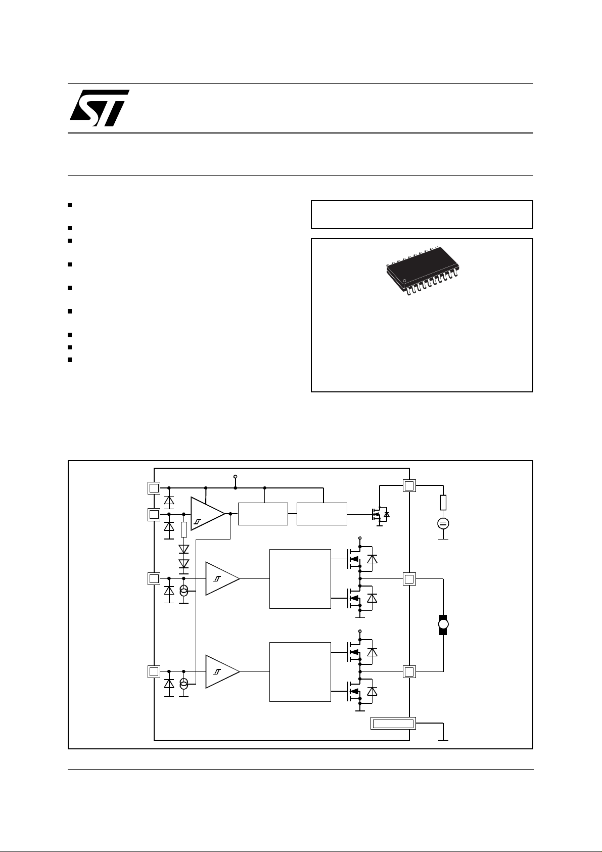
L9997ND
DUAL HALF BRIDGE DRIVER
MULTIPOWER BCD TECHNOLOGY
SO20 (12+4+4)
ORDERING NUMBERS:
L9997ND013TR
L9997ND
DESCRIPTION
The L9997ND is a monolithic integrated driver, in
BCD technology intended to drive various loads,
BLOCK DIAGRAM
VS VS
1
EN
IN1
IN2
10
12
9
ENABLE
REFERENCE
BIAS
including DC motors. The circuit is optimized for
automotive electronics enviromental conditions.
DIAG
11
PROTECTION
FUNCTIONS
DRIVER 1
DRIVER 2
VS
OUT1
19
VS
OUT2
2
5V
M
April 1999
GND
4...7, 14...17
1/9
L9997ND
ABSOLUTE MAXIMUM RATINGS
Symbol Parameter Value Unit
V
V
V
V
I
VSDC
VSP
I
OUT
IN1,2
V
EN
DIAG
I
OUT
DIAG
DC Supply Voltage -0.3 to 26 V
Supply Voltage Pulse (T < 400ms) 40 V
DC Output Current
1.8 A
±
DC Input Voltage -0.3 to 7 V
Enable Input Voltage -0.3 to 7 V
DC Output Voltage -0.3 to 7 V
DC Output Short-circuit Current -0.3V < V
< VS + 0.3V internally limited
OUT
DC Sink Current -0.3V < VDG < 7V internally limited
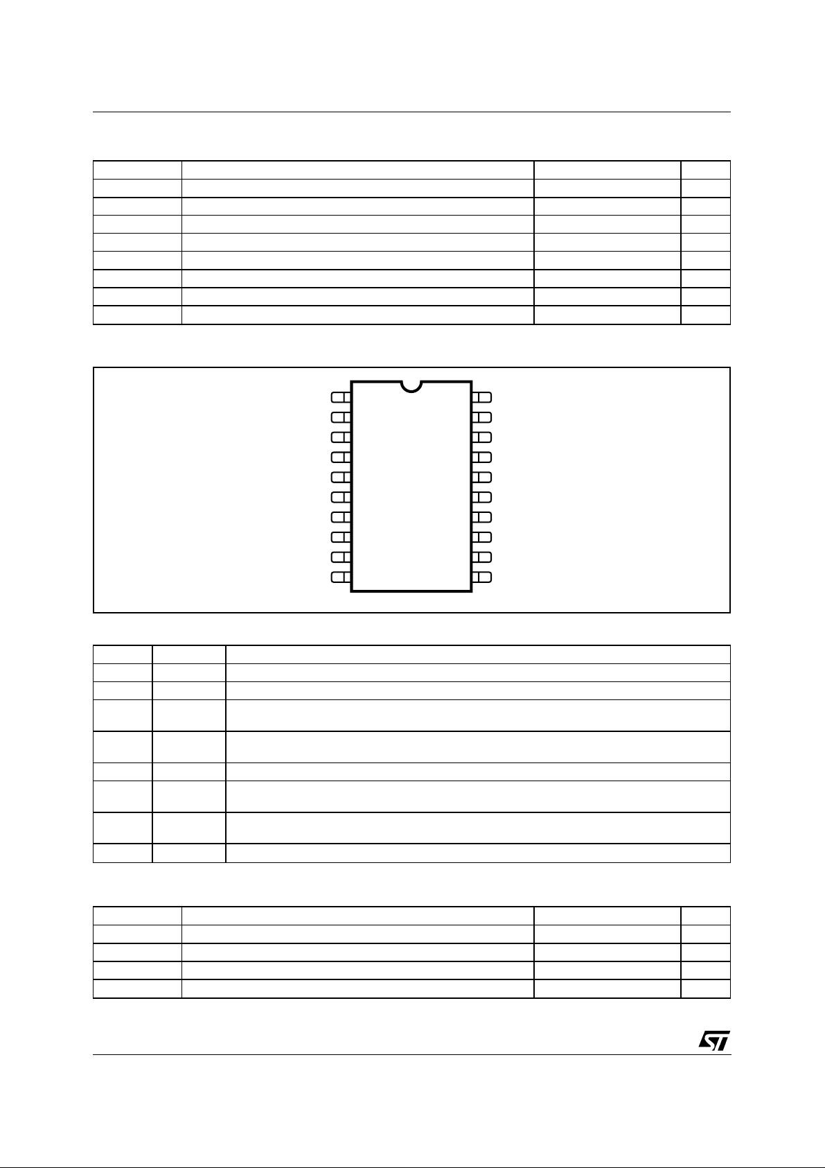
PIN CONNECTION
(Top view)
V
S
OUT2
N.C.
GND
GND
GND
GND
N.C.
IN2 IN1
EN DIAG
2
3
4
5
6
7
8
9
10
D95AT166
20
19
18
17
16
15
14
13
12
11
N.C.1
OUT1
N.C.
GND
GND
GND
GND
N.C.
PIN FUNCTIONS
N. Name Function
1 VS Supply Voltage
2 OUT2 Channel 2: Push-Pull power output with intrinsic body diode
3, 8, 13,
18,20
4 to 7,
14 to 17
9 IN2 Input 2: Schmitt Trigger input with hysteresis (non-inverting signal control)
10 EN Enable: LOW or not connected on this input switches the device into standby mode and the
11 DIAG Diagnostic: Open Drain Output that switches LOW if overvoltage or overtemperature is
12 IN1 Input 1: Schmitt Trigger input with hysteresis (non-inverting signal control)
NC NC: Not Connected
GND Ground: signal - and power - ground, heat sink
outputs into tristate
detected
THERMAL DATA
Symbol Parameter Value Unit
T
jTS
T
jTSH
R
th j-amb
R
th j-pins
(1) With 6cm2 on board heatsink area.
2/9
Thermal Shut-down Junction Temperature 165 °C
Thermal Shut-down Threshold Hysteresis 25 K
Thermal Resistance Junction-Ambient
(1)
50 K/W
Thermal Resistance Junction-Pins 15 K/W
L9997ND
ELECTRICAL CHARACTERISTICS
(7V < V
< 16.5V; -40°C < TJ < 150°C; unless otherwise specified.)
S
Symbol Parameter Test Condition Min. Typ. Max. Unit
I
VS_SB
I
VS
V
ENL
V
ENH
V
ENthh
I
EN
V
IN1,2L
V
IN1,2H
V
IN1,2thh
I
IN1,2
R
ON OUT1,2
|I
OUT1,2
V
DIAG
Quiescent Current in Standby
Mode
Supply Current EN = HIGH, I
Low Enable Voltage 1.5 V
High Enable Voltage 3.5 6 V
Enable Threshold Hysteresis 1 V
Enable Input Current VEN = 5V 85 250
Low Input Voltage 1.5 V
High Input Voltage 3.5 V
Input Threshold Hysteresis 1 V
Input Bias Current VIN = 0
ON-Resistance to Supply or
GND
| Output Current Limitation 1.2 1.6 2.2 A
Diagnostic Output Drop I
VEN < 0.3V; VVS <16.5V; Tj < 85°(*)
V
= 0; VVS = 14.5V; T
EN
OUT1,2
V
= 5V, EN = HIGH
IN
I
= ±0.8A; VVS = 7V; Tj = 125°C
OUT
I
= ±0.8A; VVS = 12V; Tj = 125°C
OUT
I
= ±0.8A; VVS = 12V; Tj = 25°C
OUT
= 0.5mA, EN = HIGH
DIAG
= 25°C
j
= 0 2 6 mA
<1
<1
-3
2
0
10
1.2
1.1
90
10
1
50
2.8
2.25
0.7
0.6 V
Overvoltage or Thermal Shutdown
V
VSOVth
Supply Overvoltage
17 19 21 V
Threshold
t
ONLH
t
ONHL
t
OFFHL
t
OFFLH
t
dHL
t
dLH
t
rHS
t
rLS
t
fHS
t
fLS
* Tested at 125°C and guaranteed by correlation
Turn on Delay Time See Fig. 2; VVS = 13.5V
Measured with 93Ω load
50 150
30 150
Turn off Delay Time 10 100
220
Rising Delay Time 115 250
Falling Delay Time 115 250
Rise Time 30 100
60 150
Fall Time 25 100
50 150
A
µ
A
µ
A
µ
A
µ
A
µ
Ω
Ω
Ω
s
µ
s
µ
s
µ
s
µ
s
µ
s
µ
s
µ
s
µ
s
µ
s
µ
FUNCTIONAL DESCRIPTION
The L9997ND is a motor driver two half-bridge
outputs, intended for driving dc motors in automotive systems. The basic function of the device is
shown in the Table 1.
Table 1. Table function.
Status EN IN1 IN2 OUT1 OUT2 DIAG NOTE
1 L X X Tristate Tristate OFF Standby Mode
2 H H H SRC SRC OFF Recommended for braking
3 H H L SRC SNK OFF
4HLHSNKSRCOFF
5 H L L SNK SNK OFF
6 H X X Tristate Tristate ON Overvoltage or Overtemperature
3/9

L9997ND
The device is activated with enable input voltage
HIGH. For enable input floating (not connected)
or LOW the device is in Standby Mode. Very low
quiescent current is defined for V
< 0.3V. When
EN
activating or disactivating the device by the enable input a wake-up time of 50µs is recommended.
For braking of the motor the status 2 is recommended. The reason for this recommendation is
that the device features higher threshold for initialisation of parasitic structures than in state 5.
The inputs IN1, IN2 features internal s ink current
generators of 10µA, disabled in standby mode.
With these input current generators the input level
is forced to LOW for inputs open. In this condition
the outputs are in SNK state.
The circuit features an over voltage disable function referred to the supply voltage V
. This func-
VS
tion assures disabling the power outputs, when
the supply voltage exceeds the over voltage
threshold value of 19V typ. Both outputs are
forced to tristate in this condition and the diagnostic output is ON.
The thermal shut-down disables the outputs (tristate) and activates the diagnostic when the junction temperature increases above the thermal
shut-down threshold temperature of min. 150°C.
For the start of a heavy loaded motor, if t he m otor
current reaches the max. value, it is necessary to
respect the dynamical thermal resistance junction
to ambient. The outputs OUT1 and OUT2 are protected against short circuit to GND or V
, for sup-
S
ply voltages up to the overvoltage disable threshold.
The output power DMOS transistors works in linear mode for an output current less than 1.2A. Increasing the output load current ( > 1.2A) the out-
put transistor changes in the current regulation
mode, see Fig.6, with the typical output current
value below 2A. The SRC output power DMOS
transistors requires a voltage drop ~3V to activate
the current regulation. Below this voltage drop is
the device also protected. The output current heat
up the power DMOS transistor, the R
DSON
increases with the junction temperature and decreases the output current. The power dissipation
in this condition can activate the thermal shutdown . In the case of output disable due to thermal overload the output remains disabled untill
the junction temperature decreases under the
thermal enable threshold.
Permanent short circuit condition with power dissipation leading to chip overheating and activation
of the thermal shut- down leads to t he thermal oscillation. The junction temperature difference between the switch ON and OFF points is the thermal hysteresis of the thermal protection. This
hysteresis together with the thermal impedance
and ambient temperature determines the frequency of this thermal oscillation, its typical values are in the range of 10kHz.
The open drain diagnostic output needs an external pull-up resistor to a 5V supply. In systems
with several L9997ND the diagnostic outputs can
be connected together with a common pull-up resistor. The DIAG output current is internally limited.
Fig. 1 shows a typical application diagram for the
DC motor driving. To assure the safety of the circuit in the reverse battery condition a reverse protection diode D
is necessary. The transient pro-
1
tection diode D2 must assure that the maximal
supply voltage V
line will be limited to a value lower than the
V
BAT
during the transients at the
VS
absolute maximum rating for VVS.
Figure 1:
5V
4/9
Application Circuit Diagram.
CONTROL
LOGIC
Ω
47K
IDIAG1
IIN1
IIN2
IEN
DIAG1
IN1
IN2
EN
S
V
L9997ND
GND
I
s
S
C
OUT1
IOUT1
OUT2
IOUT2
1
D
V
BAT
2
D
IM
VM
M
GND

Figure 2. Timing Diagram.
L9997ND
Standby Mode Operating Mode Overtemperature
EN
IN1
IN2
DIAG
OUT1
OUT2
Tristate
Tristate
t
10%
dLH
90%
t
r
t
dHL
t
t
ONHL
t
ONLH
90%
50%
10%
t
rf
t
dHL
t
f
t
dLH
or Overvoltage
t
dLH
Tristate
t
dHL
Tristate
t
t
dHL
dLH
Standby Mode
t
OFFLH
Tristate
t
OFFHL
Tristate
Figure 3. Typical RON - Characteristics of Source and Sink Stage
5/9

L9997ND
Figure 4. Quiescent current in standby mode versus supply voltage.
Figure 5. ON-Resistance versus supply voltage.
6/9

L9997ND
Figure 6. I
versus V
OUT
(pulsed measurement with TON = 500µs, T
OUT
= 500ms).
OFF
Figure 7. Test circuit.
12V
V
EN
V
IN1
100µF
V
IN2
200nF
EN
IN1
IN2
VS
L9997ND
GND
DIAG
OUT1
OUT2
10k
15
15
Ω
Ω
Ω
5V
7/9

L9997ND
8/9

L9997ND
Information furnishe d is beli eved to be accu rate and reliable. However, STMicroelec tronics assumes no res ponsibility for the consequences
of use of such i nformation nor for any i nfringement of patents or ot her rights of third par ties which may result from its use. No license i s
granted by impli cation or otherwis e under any patent or patent righ ts of STMicroelect ronics. Specifica tion mentioned in this publication are
subject to change without notic e. This public ation supers edes and replaces all information prev iously supplied. STMic roelec tronic s products
are not authorized for use as critical components in life support devices or systems without express written approval of STMicroelectronics.
The ST logo is a registered trademark of STMicroelect roni cs
© 1999 STMicroelectronics – Printed in Italy – All Rights Reserved
STMicroelectronics GROUP OF COMPANIES
Australia - Brazil - Canada - China - France - Germany - Italy - Japan - Korea - Malaysia - Malta - Mexico - Morocco - The Netherlands -
Singapore - Spain - Sweden - Switzerland - Taiwan - Thailand - United Kingdom - U.S.A.
http://www.st.com
9/9
 Loading...