

Page 1
Features
■ Two 5V low-drop voltage regulators (250mA,
100mA continuous mode
■ Low stand-by current: V
45µA, (75µA in cycl. sense)
■ Window watchdog and fail-safe output
■ Interrupt output
■ Wake-up logic with cyclic contact monitoring
■ LIN 2.1 compliant (SAEJ2602 compatible)
transceiver
■ 24 bit SPI interface for mode control and
diagnostic
■ Output drivers
■ 4 High side drivers for e.g. LED or HALL
(R
DSon,typ
= 7 Ω )
■ 1 High side driver Out_HS ( R
■ 2 Relay drivers ( R
DSon,typ
■ Outputs are short circuit protected
■ 2 Op amp's for current sensing in GND return
lines
■ Temperature warning and thermal shutdown
Table 1. Device summary
stby, 7µA; ,V1 stby,
BAT
DSon,typ
= 2 Ω )
= 1 Ω )
L9952GXP
Power management system IC
PowerSSO-36
Applications
■ Automotive ECU’ s such as door zone and
body control modules.
Description
The L9952GXP is a power management system
IC containing two low drop regulators with
advanced contact monitoring and additional
peripheral functions.
The integrated standard serial peripheral interface
(SPI) controls all L9952GXP operation modes
and provides driver diagnostic functions.
Order codes
Package
Tube Tape and reel
PowerSSO-36 L9952GXP L9952GXPTR
July 2009 Doc ID 13518 Rev 5 1/68
www.st.com
1
Page 2

Contents L9952GXP
Contents
1 Pin definitions and functions . . . . . . . . . . . . . . . . . . . . . . . . . . . . . . . . . . 8
2 Description . . . . . . . . . . . . . . . . . . . . . . . . . . . . . . . . . . . . . . . . . . . . . . . . 11
2.1 Voltage regulator . . . . . . . . . . . . . . . . . . . . . . . . . . . . . . . . . . . . . . . . . . . 11
2.1.1 Voltage regulator: V1 . . . . . . . . . . . . . . . . . . . . . . . . . . . . . . . . . . . . . . . 11
2.1.2 Voltage regulator: V2 . . . . . . . . . . . . . . . . . . . . . . . . . . . . . . . . . . . . . . . 11
2.2 Power control in operating modes . . . . . . . . . . . . . . . . . . . . . . . . . . . . . . 12
2.2.1 Active mode . . . . . . . . . . . . . . . . . . . . . . . . . . . . . . . . . . . . . . . . . . . . . . 12
2.2.2 Flash mode . . . . . . . . . . . . . . . . . . . . . . . . . . . . . . . . . . . . . . . . . . . . . . 12
2.2.3 V1 standby mode . . . . . . . . . . . . . . . . . . . . . . . . . . . . . . . . . . . . . . . . . . 12
2.2.4 VBAT standby mode . . . . . . . . . . . . . . . . . . . . . . . . . . . . . . . . . . . . . . . 12
2.3 Wake up events . . . . . . . . . . . . . . . . . . . . . . . . . . . . . . . . . . . . . . . . . . . . 13
2.4 Functional overview (truth table) . . . . . . . . . . . . . . . . . . . . . . . . . . . . . . . 14
2.5 Wake up inputs . . . . . . . . . . . . . . . . . . . . . . . . . . . . . . . . . . . . . . . . . . . . . 16
2.6 Hall sensor ports: WU3,4, Dig_Out 3,4 . . . . . . . . . . . . . . . . . . . . . . . . . . 16
2.7 Interrupt . . . . . . . . . . . . . . . . . . . . . . . . . . . . . . . . . . . . . . . . . . . . . . . . . . 17
2.8 Cyclic contact supply . . . . . . . . . . . . . . . . . . . . . . . . . . . . . . . . . . . . . . . . 17
2.9 Window – watchdog . . . . . . . . . . . . . . . . . . . . . . . . . . . . . . . . . . . . . . . . . 17
2.10 Fail safe output . . . . . . . . . . . . . . . . . . . . . . . . . . . . . . . . . . . . . . . . . . . . . 19
2.11 Reset – generator . . . . . . . . . . . . . . . . . . . . . . . . . . . . . . . . . . . . . . . . . . . 19
2.12 V1, V2 fail . . . . . . . . . . . . . . . . . . . . . . . . . . . . . . . . . . . . . . . . . . . . . . . . . 20
2.13 Low side driver outputs Rel1, Rel2 . . . . . . . . . . . . . . . . . . . . . . . . . . . . . . 20
2.14 PWM inputs . . . . . . . . . . . . . . . . . . . . . . . . . . . . . . . . . . . . . . . . . . . . . . . 20
2.15 Operational amplifiers . . . . . . . . . . . . . . . . . . . . . . . . . . . . . . . . . . . . . . . 21
2.16 LIN bus interface . . . . . . . . . . . . . . . . . . . . . . . . . . . . . . . . . . . . . . . . . . . 21
2.17 Error handling . . . . . . . . . . . . . . . . . . . . . . . . . . . . . . . . . . . . . . . . . . . . . . 22
2.17.1 Dominant TxD time out . . . . . . . . . . . . . . . . . . . . . . . . . . . . . . . . . . . . . 22
2.17.2 Short to battery time out . . . . . . . . . . . . . . . . . . . . . . . . . . . . . . . . . . . . 22
2.17.3 Short to ground mode . . . . . . . . . . . . . . . . . . . . . . . . . . . . . . . . . . . . . . 22
2.18 Wake up (from LIN) . . . . . . . . . . . . . . . . . . . . . . . . . . . . . . . . . . . . . . . . . 22
2.18.1 Normal wake up . . . . . . . . . . . . . . . . . . . . . . . . . . . . . . . . . . . . . . . . . . . 22
2.18.2 Wake up from short to GND condition . . . . . . . . . . . . . . . . . . . . . . . . . . 22
2/68 Doc ID 13518 Rev 5
Page 3

L9952GXP Contents
2.18.3 RxD pin in V1 standby . . . . . . . . . . . . . . . . . . . . . . . . . . . . . . . . . . . . . . 22
2.19 LINPU . . . . . . . . . . . . . . . . . . . . . . . . . . . . . . . . . . . . . . . . . . . . . . . . . . . . 23
2.20 Serial Peripheral Interface (SPI) . . . . . . . . . . . . . . . . . . . . . . . . . . . . . . . . 23
2.20.1 Chip Select Not (CSN) . . . . . . . . . . . . . . . . . . . . . . . . . . . . . . . . . . . . . . 23
2.20.2 Serial Data In (DI) . . . . . . . . . . . . . . . . . . . . . . . . . . . . . . . . . . . . . . . . . 24
2.20.3 Serial Data Out (DO) . . . . . . . . . . . . . . . . . . . . . . . . . . . . . . . . . . . . . . . 24
2.20.4 Serial Clock (CLK) . . . . . . . . . . . . . . . . . . . . . . . . . . . . . . . . . . . . . . . . . 24
2.20.5 Data registers . . . . . . . . . . . . . . . . . . . . . . . . . . . . . . . . . . . . . . . . . . . . 24
3 Protection and diagnosis . . . . . . . . . . . . . . . . . . . . . . . . . . . . . . . . . . . . 25
3.1 Power supply fail . . . . . . . . . . . . . . . . . . . . . . . . . . . . . . . . . . . . . . . . . . . 25
3.1.1 Over voltage . . . . . . . . . . . . . . . . . . . . . . . . . . . . . . . . . . . . . . . . . . . . . . 25
3.1.2 Under voltage . . . . . . . . . . . . . . . . . . . . . . . . . . . . . . . . . . . . . . . . . . . . . 25
3.2 Temperature warning and thermal shutdown . . . . . . . . . . . . . . . . . . . . . . 25
3.3 SPI diagnosis . . . . . . . . . . . . . . . . . . . . . . . . . . . . . . . . . . . . . . . . . . . . . . 25
3.4 High side driver outputs . . . . . . . . . . . . . . . . . . . . . . . . . . . . . . . . . . . . . . 27
3.5 Low side driver outputs Rel1, Rel2 . . . . . . . . . . . . . . . . . . . . . . . . . . . . . . 27
4 Absolute maximum ratings . . . . . . . . . . . . . . . . . . . . . . . . . . . . . . . . . . 28
5 ESD protection . . . . . . . . . . . . . . . . . . . . . . . . . . . . . . . . . . . . . . . . . . . . 29
6 Thermal data . . . . . . . . . . . . . . . . . . . . . . . . . . . . . . . . . . . . . . . . . . . . . . 30
6.1 Operating junction temperature . . . . . . . . . . . . . . . . . . . . . . . . . . . . . . . . 30
6.2 Temperature warning and thermal shutdown . . . . . . . . . . . . . . . . . . . . . . 30
6.3 Package and PCB thermal data . . . . . . . . . . . . . . . . . . . . . . . . . . . . . . . . 31
7 Electrical characteristics . . . . . . . . . . . . . . . . . . . . . . . . . . . . . . . . . . . . 34
7.1 Supply and supply monitoring . . . . . . . . . . . . . . . . . . . . . . . . . . . . . . . . . 34
7.2 Oscillator . . . . . . . . . . . . . . . . . . . . . . . . . . . . . . . . . . . . . . . . . . . . . . . . . 35
7.3 Power-on reset (Vs) . . . . . . . . . . . . . . . . . . . . . . . . . . . . . . . . . . . . . . . . . 35
7.4 Voltage regulator V1 . . . . . . . . . . . . . . . . . . . . . . . . . . . . . . . . . . . . . . . . . 35
7.5 Voltage regulator V2 . . . . . . . . . . . . . . . . . . . . . . . . . . . . . . . . . . . . . . . . . 36
7.6 Reset generator (V1 supervision) . . . . . . . . . . . . . . . . . . . . . . . . . . . . . . 37
7.7 Watchdog . . . . . . . . . . . . . . . . . . . . . . . . . . . . . . . . . . . . . . . . . . . . . . . . . 37
Doc ID 13518 Rev 5 3/68
Page 4

Contents L9952GXP
7.8 High side outputs . . . . . . . . . . . . . . . . . . . . . . . . . . . . . . . . . . . . . . . . . . . 39
7.8.1 Output (Out_HS) . . . . . . . . . . . . . . . . . . . . . . . . . . . . . . . . . . . . . . . . . . 39
7.8.2 Outputs (OUT1...4) . . . . . . . . . . . . . . . . . . . . . . . . . . . . . . . . . . . . . . . . 40
7.9 Relay drivers . . . . . . . . . . . . . . . . . . . . . . . . . . . . . . . . . . . . . . . . . . . . . . 40
7.10 Wake up inputs ( WU1..WU4) . . . . . . . . . . . . . . . . . . . . . . . . . . . . . . . . . 41
7.11 Wake up input (INH) . . . . . . . . . . . . . . . . . . . . . . . . . . . . . . . . . . . . . . . . . 42
7.12 LIN . . . . . . . . . . . . . . . . . . . . . . . . . . . . . . . . . . . . . . . . . . . . . . . . . . . . . . 42
7.13 Operational amplifier . . . . . . . . . . . . . . . . . . . . . . . . . . . . . . . . . . . . . . . . 47
7.14 SPI . . . . . . . . . . . . . . . . . . . . . . . . . . . . . . . . . . . . . . . . . . . . . . . . . . . . . . 48
7.14.1 Input: CSN . . . . . . . . . . . . . . . . . . . . . . . . . . . . . . . . . . . . . . . . . . . . . . . 48
7.14.2 Inputs: CLK, DI, PWM 1, PWM 2 . . . . . . . . . . . . . . . . . . . . . . . . . . . . . . 48
7.14.3 Input PWM 2 Vth for flash mode . . . . . . . . . . . . . . . . . . . . . . . . . . . . . . 49
7.14.4 DI timing . . . . . . . . . . . . . . . . . . . . . . . . . . . . . . . . . . . . . . . . . . . . . . . . . 49
7.14.5 DO, FSO, Dig_Out3,4 . . . . . . . . . . . . . . . . . . . . . . . . . . . . . . . . . . . . . . 50
7.14.6 DO timing . . . . . . . . . . . . . . . . . . . . . . . . . . . . . . . . . . . . . . . . . . . . . . . . 50
7.14.7 CSN timing . . . . . . . . . . . . . . . . . . . . . . . . . . . . . . . . . . . . . . . . . . . . . . . 51
8 SPI control and status registers . . . . . . . . . . . . . . . . . . . . . . . . . . . . . . 54
8.1 SPI registers . . . . . . . . . . . . . . . . . . . . . . . . . . . . . . . . . . . . . . . . . . . . . . . 54
8.1.1 Control register 0 . . . . . . . . . . . . . . . . . . . . . . . . . . . . . . . . . . . . . . . . . . 55
8.1.2 Control register 1 . . . . . . . . . . . . . . . . . . . . . . . . . . . . . . . . . . . . . . . . . . 56
8.1.3 Control register 2 . . . . . . . . . . . . . . . . . . . . . . . . . . . . . . . . . . . . . . . . . . 59
8.1.4 Status register 0 . . . . . . . . . . . . . . . . . . . . . . . . . . . . . . . . . . . . . . . . . . . 61
8.1.5 Status register 1 . . . . . . . . . . . . . . . . . . . . . . . . . . . . . . . . . . . . . . . . . . . 62
9 Package and packing information . . . . . . . . . . . . . . . . . . . . . . . . . . . . . 64
9.1 ECOPACK® packages . . . . . . . . . . . . . . . . . . . . . . . . . . . . . . . . . . . . . . . 64
9.2 PowerSSO-36 package information . . . . . . . . . . . . . . . . . . . . . . . . . . . . . 64
9.3 PowerSSO-36 packing information . . . . . . . . . . . . . . . . . . . . . . . . . . . . . 66
10 Revision history . . . . . . . . . . . . . . . . . . . . . . . . . . . . . . . . . . . . . . . . . . . 67
4/68 Doc ID 13518 Rev 5
Page 5

L9952GXP List of tables
List of tables
Table 1. Device summary . . . . . . . . . . . . . . . . . . . . . . . . . . . . . . . . . . . . . . . . . . . . . . . . . . . . . . . . . . 1
Table 2. Pins definitions and functions . . . . . . . . . . . . . . . . . . . . . . . . . . . . . . . . . . . . . . . . . . . . . . . . 8
Table 4. Functional overview (truth table). . . . . . . . . . . . . . . . . . . . . . . . . . . . . . . . . . . . . . . . . . . . . 14
Table 5. Absolute maximum ratings . . . . . . . . . . . . . . . . . . . . . . . . . . . . . . . . . . . . . . . . . . . . . . . . . 28
Table 6. ESD protection . . . . . . . . . . . . . . . . . . . . . . . . . . . . . . . . . . . . . . . . . . . . . . . . . . . . . . . . . . 29
Table 7. Operating junction temperature . . . . . . . . . . . . . . . . . . . . . . . . . . . . . . . . . . . . . . . . . . . . . 30
Table 8. Temperature warning and thermal shutdown . . . . . . . . . . . . . . . . . . . . . . . . . . . . . . . . . . . 30
Table 9. Thermal parameters . . . . . . . . . . . . . . . . . . . . . . . . . . . . . . . . . . . . . . . . . . . . . . . . . . . . . . 33
Table 10. Supply and supply monitoring. . . . . . . . . . . . . . . . . . . . . . . . . . . . . . . . . . . . . . . . . . . . . . . 34
Table 11. Oscillator . . . . . . . . . . . . . . . . . . . . . . . . . . . . . . . . . . . . . . . . . . . . . . . . . . . . . . . . . . . . . . . 35
Table 12. Power-on Reset (Vs) . . . . . . . . . . . . . . . . . . . . . . . . . . . . . . . . . . . . . . . . . . . . . . . . . . . . . 35
Table 13. Voltage regulator V1 . . . . . . . . . . . . . . . . . . . . . . . . . . . . . . . . . . . . . . . . . . . . . . . . . . . . . . 35
Table 14. Voltage regulator V2 . . . . . . . . . . . . . . . . . . . . . . . . . . . . . . . . . . . . . . . . . . . . . . . . . . . . . . 36
Table 15. Reset generator . . . . . . . . . . . . . . . . . . . . . . . . . . . . . . . . . . . . . . . . . . . . . . . . . . . . . . . . . 37
Table 16. Watchdog . . . . . . . . . . . . . . . . . . . . . . . . . . . . . . . . . . . . . . . . . . . . . . . . . . . . . . . . . . . . . . 37
Table 17. High side outputs (Out_HS) . . . . . . . . . . . . . . . . . . . . . . . . . . . . . . . . . . . . . . . . . . . . . . . . 39
Table 18. High side outputs (OUT 1..4) . . . . . . . . . . . . . . . . . . . . . . . . . . . . . . . . . . . . . . . . . . . . . . . 40
Table 19. Relay drivers . . . . . . . . . . . . . . . . . . . . . . . . . . . . . . . . . . . . . . . . . . . . . . . . . . . . . . . . . . . . 40
Table 20. Wake up inputs(WU1...WU4) . . . . . . . . . . . . . . . . . . . . . . . . . . . . . . . . . . . . . . . . . . . . . . . 41
Table 21. Wake up input (INH) . . . . . . . . . . . . . . . . . . . . . . . . . . . . . . . . . . . . . . . . . . . . . . . . . . . . . . 42
Table 22. LIN receiver . . . . . . . . . . . . . . . . . . . . . . . . . . . . . . . . . . . . . . . . . . . . . . . . . . . . . . . . . . . . 42
Table 23. LIN DC parameters . . . . . . . . . . . . . . . . . . . . . . . . . . . . . . . . . . . . . . . . . . . . . . . . . . . . . . . 43
Table 24. LIN transmitter . . . . . . . . . . . . . . . . . . . . . . . . . . . . . . . . . . . . . . . . . . . . . . . . . . . . . . . . . . 44
Table 25. LIN timing . . . . . . . . . . . . . . . . . . . . . . . . . . . . . . . . . . . . . . . . . . . . . . . . . . . . . . . . . . . . . . 44
Table 26. LIN DC values. . . . . . . . . . . . . . . . . . . . . . . . . . . . . . . . . . . . . . . . . . . . . . . . . . . . . . . . . . . 45
Table 27. Operational amplifier. . . . . . . . . . . . . . . . . . . . . . . . . . . . . . . . . . . . . . . . . . . . . . . . . . . . . . 47
Table 28. SPI (Input CSN) . . . . . . . . . . . . . . . . . . . . . . . . . . . . . . . . . . . . . . . . . . . . . . . . . . . . . . . . . 48
Table 29. Inputs: CLK, DI, PWM 1, PWM 2 . . . . . . . . . . . . . . . . . . . . . . . . . . . . . . . . . . . . . . . . . . . . 48
Table 30. Input PWM2 Vth for flash mode . . . . . . . . . . . . . . . . . . . . . . . . . . . . . . . . . . . . . . . . . . . . . 49
Table 31. DI timing . . . . . . . . . . . . . . . . . . . . . . . . . . . . . . . . . . . . . . . . . . . . . . . . . . . . . . . . . . . . . . . 49
Table 32. DO, FSO, Digout3,4 . . . . . . . . . . . . . . . . . . . . . . . . . . . . . . . . . . . . . . . . . . . . . . . . . . . . . . 50
Table 33. DO timing . . . . . . . . . . . . . . . . . . . . . . . . . . . . . . . . . . . . . . . . . . . . . . . . . . . . . . . . . . . . . . 50
Table 34. CSN timing . . . . . . . . . . . . . . . . . . . . . . . . . . . . . . . . . . . . . . . . . . . . . . . . . . . . . . . . . . . . . 51
Table 35. SPI registers . . . . . . . . . . . . . . . . . . . . . . . . . . . . . . . . . . . . . . . . . . . . . . . . . . . . . . . . . . . . 54
Table 36. Control register 0 . . . . . . . . . . . . . . . . . . . . . . . . . . . . . . . . . . . . . . . . . . . . . . . . . . . . . . . . 55
Table 37. Configuration bit HSxx . . . . . . . . . . . . . . . . . . . . . . . . . . . . . . . . . . . . . . . . . . . . . . . . . . . . 55
Table 38. Configuration bit OUT_HSx . . . . . . . . . . . . . . . . . . . . . . . . . . . . . . . . . . . . . . . . . . . . . . . . 55
Table 39. Configuration bit RELx . . . . . . . . . . . . . . . . . . . . . . . . . . . . . . . . . . . . . . . . . . . . . . . . . . . . 55
Table 40. Configuration bit On_V2x . . . . . . . . . . . . . . . . . . . . . . . . . . . . . . . . . . . . . . . . . . . . . . . . . . 55
Table 41. Configuration bit TRIG, GO_VBAT, GO_V1 . . . . . . . . . . . . . . . . . . . . . . . . . . . . . . . . . . . . 56
Table 42. Control register 1 . . . . . . . . . . . . . . . . . . . . . . . . . . . . . . . . . . . . . . . . . . . . . . . . . . . . . . . . 56
Table 43. Configuration bit Wx . . . . . . . . . . . . . . . . . . . . . . . . . . . . . . . . . . . . . . . . . . . . . . . . . . . . . . 56
Table 44. Configuration bit Ux . . . . . . . . . . . . . . . . . . . . . . . . . . . . . . . . . . . . . . . . . . . . . . . . . . . . . . 57
Table 45. Configuration bit Lx . . . . . . . . . . . . . . . . . . . . . . . . . . . . . . . . . . . . . . . . . . . . . . . . . . . . . . . 57
Table 46. Configuration bit Txx. . . . . . . . . . . . . . . . . . . . . . . . . . . . . . . . . . . . . . . . . . . . . . . . . . . . . . 58
Table 47. Configuration bit INT_enable . . . . . . . . . . . . . . . . . . . . . . . . . . . . . . . . . . . . . . . . . . . . . . . 58
Table 48. Control register 2 . . . . . . . . . . . . . . . . . . . . . . . . . . . . . . . . . . . . . . . . . . . . . . . . . . . . . . . . 59
Table 49. Configuration bit OLT_HSx, VSLOCK Out, O_HS_REC, LINPU and TXD_TOUT. . . . . . . 59
Doc ID 13518 Rev 5 5/68
Page 6

List of tables L9952GXP
Table 50. Configuration bit LEVx . . . . . . . . . . . . . . . . . . . . . . . . . . . . . . . . . . . . . . . . . . . . . . . . . . . . 59
Table 51. Configuration bit ICxx . . . . . . . . . . . . . . . . . . . . . . . . . . . . . . . . . . . . . . . . . . . . . . . . . . . . . 60
Table 52. Configuration bit LIN slope, LS_ovuv and ICMP . . . . . . . . . . . . . . . . . . . . . . . . . . . . . . . . 60
Table 53. Status register 0 . . . . . . . . . . . . . . . . . . . . . . . . . . . . . . . . . . . . . . . . . . . . . . . . . . . . . . . . . 61
Table 54. Configuration bit HSx_OL, HSx_OC and Relx_OC . . . . . . . . . . . . . . . . . . . . . . . . . . . . . . 61
Table 55. Configuration bit SHT5V2, WUx, INH, LIN and Cold Start . . . . . . . . . . . . . . . . . . . . . . . . . 61
Table 56. Status register 1 . . . . . . . . . . . . . . . . . . . . . . . . . . . . . . . . . . . . . . . . . . . . . . . . . . . . . . . . . 62
Table 57. Configuration bit OV, UV, TW, TSDx and Vx Fail . . . . . . . . . . . . . . . . . . . . . . . . . . . . . . . . 62
Table 58. Configuration bit STx . . . . . . . . . . . . . . . . . . . . . . . . . . . . . . . . . . . . . . . . . . . . . . . . . . . . . 62
Table 59. Configuration bit Rx, WDx, TRIG, SHT_GND, SHT_BAT and DOM_TXD . . . . . . . . . . . . . 63
Table 60. PowerSSO-36 mechanical data . . . . . . . . . . . . . . . . . . . . . . . . . . . . . . . . . . . . . . . . . . . . . 64
Table 61. Document revision history . . . . . . . . . . . . . . . . . . . . . . . . . . . . . . . . . . . . . . . . . . . . . . . . . 67
6/68 Doc ID 13518 Rev 5
Page 7

L9952GXP List of figures
List of figures
Figure 1. Block diagram . . . . . . . . . . . . . . . . . . . . . . . . . . . . . . . . . . . . . . . . . . . . . . . . . . . . . . . . . . . . 8
Figure 2. Pins configuration . . . . . . . . . . . . . . . . . . . . . . . . . . . . . . . . . . . . . . . . . . . . . . . . . . . . . . . . 10
Figure 3. Operating modes, main states . . . . . . . . . . . . . . . . . . . . . . . . . . . . . . . . . . . . . . . . . . . . . . 15
Figure 4. Watchdog . . . . . . . . . . . . . . . . . . . . . . . . . . . . . . . . . . . . . . . . . . . . . . . . . . . . . . . . . . . . . . 18
Figure 5. FSO . . . . . . . . . . . . . . . . . . . . . . . . . . . . . . . . . . . . . . . . . . . . . . . . . . . . . . . . . . . . . . . . . . 19
Figure 6. NReset . . . . . . . . . . . . . . . . . . . . . . . . . . . . . . . . . . . . . . . . . . . . . . . . . . . . . . . . . . . . . . . . 19
Figure 7. Lin master pull up . . . . . . . . . . . . . . . . . . . . . . . . . . . . . . . . . . . . . . . . . . . . . . . . . . . . . . . . 21
Figure 8. Protection and diagnosis . . . . . . . . . . . . . . . . . . . . . . . . . . . . . . . . . . . . . . . . . . . . . . . . . . 26
Figure 9. PowerSSO-36 PC board. . . . . . . . . . . . . . . . . . . . . . . . . . . . . . . . . . . . . . . . . . . . . . . . . . . 31
Figure 10. PowerSSO-36 thermal resistance junction ambient Vs. PCB copper area (V1 ON) . . . . . 32
Figure 11. PowerSSO-36 thermal impedance junction ambient single pulse (V1 ON) . . . . . . . . . . . . 32
Figure 12. PowerSSO-36 thermal fitting model (V1 ON) . . . . . . . . . . . . . . . . . . . . . . . . . . . . . . . . . . . 33
Figure 13. Watchdog timing . . . . . . . . . . . . . . . . . . . . . . . . . . . . . . . . . . . . . . . . . . . . . . . . . . . . . . . . . 38
Figure 14. Watchdog, closed and open window tolerances and save trigger area . . . . . . . . . . . . . . . 39
Figure 15. LIN transmit, receive timing . . . . . . . . . . . . . . . . . . . . . . . . . . . . . . . . . . . . . . . . . . . . . . . . 46
Figure 16. SPI - Input timing . . . . . . . . . . . . . . . . . . . . . . . . . . . . . . . . . . . . . . . . . . . . . . . . . . . . . . . . 51
Figure 17. SPI - Edges timing . . . . . . . . . . . . . . . . . . . . . . . . . . . . . . . . . . . . . . . . . . . . . . . . . . . . . . . 52
Figure 18. SPI - CSN low to high transition . . . . . . . . . . . . . . . . . . . . . . . . . . . . . . . . . . . . . . . . . . . . . 53
Figure 19. SPI - High to low transition . . . . . . . . . . . . . . . . . . . . . . . . . . . . . . . . . . . . . . . . . . . . . . . . . 53
Figure 20. PowerSSO-36 package dimensions . . . . . . . . . . . . . . . . . . . . . . . . . . . . . . . . . . . . . . . . . . 64
Figure 21. PowerSSO-36
Figure 22. PowerSSO-36
tube shipment (no suffix). . . . . . . . . . . . . . . . . . . . . . . . . . . . . . . . . . . . . . . 66
tape and reel shipment (suffix “TR”) . . . . . . . . . . . . . . . . . . . . . . . . . . . . . . 66
Doc ID 13518 Rev 5 7/68
Page 8
Pin definitions and functions L9952GXP
1 Pin definitions and functions
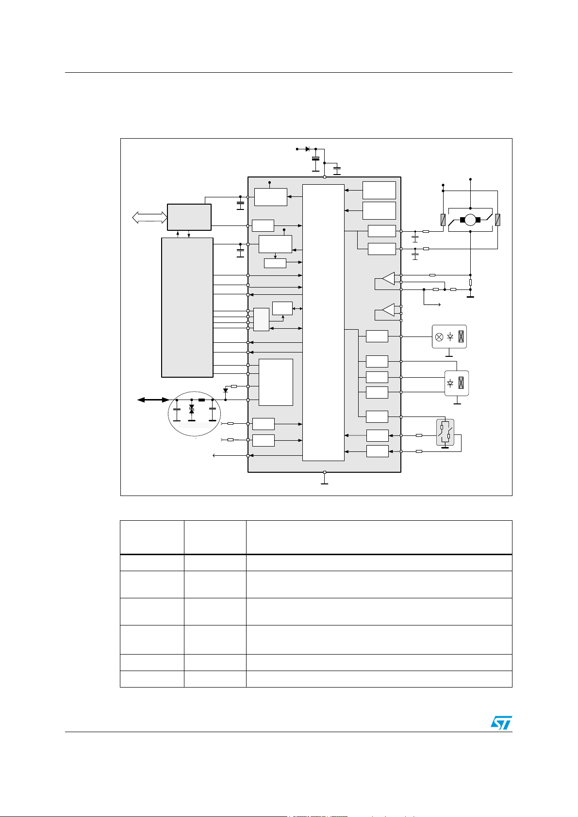
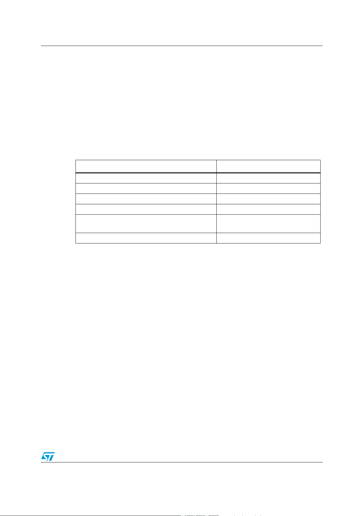
Figure 1. Block diagram
V
V
s
Voltage
Voltage
Regulator 1
Voltage
Monitor
Windo w
Watchd og
LIN 2. 1
SAEJ2602
1)
LIN 2.1 certified
Bat
V
s
Temp Pr ewarnin g
& Shutdown
Under volta ge -
Overvolt age -
Shutdown
R
Output Clamp
Output Clamp
+
-
+
-
Rel1
Rel2
OP1+
OP1OP1o u t
OP2+
OP2OP2o u t
OUT_H S
Out 1
Out 2
Out 3
Out 4
WU1
WU2
C
R
C
V
s
LOGIC
1)
Low S ide
Low S ide
High Side
High Side
High Side
High Side
High Side
Wake Up IN
Wake Up IN
V
S
µC (A DC)
V
Bat
M
e. g . Bu lb,
LED, Hall
Sensor
e. g. LED,
Hall Sensor
Cyclic Contact
Moni tori ng
CAN
LIN
For detailed information
see
EMC tes t report from
IBEE Zwickau
CAN
Microcontroller
ESDLIN1524BJ
Fail-safe Logic
220nF
INH
220nF
PWM1
PWM2
NReset
CSN
CLK
DO
Dig_Out3
Dig_Out 4 /
Inter rupt
TxD
RxD
LINPU
LIN
WU3
WU4
FSO
V2
Regulator 2
Wake Up IN
V1
SPI
DI
Wake Up IN
Wake Up IN
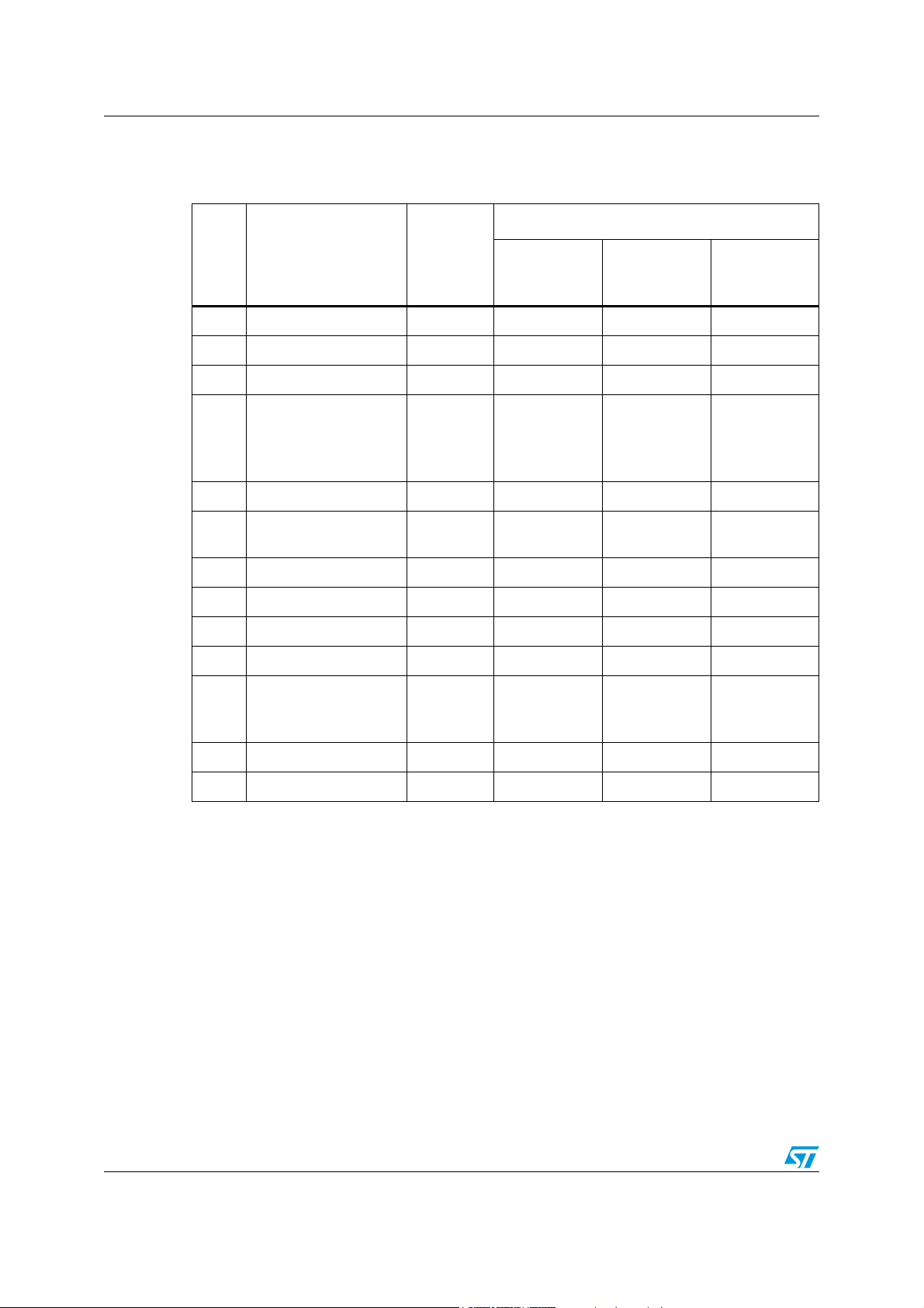
Table 2. Pins definitions and functions
Pin
name
PowerSS0-36 Function
GND 1 Ground
V2 2
V1 3
NReset 4
Voltage regulator 2 output : 5 V supply for external loads e.g. IR
receiver, potentiometer
Voltage regulator 1 output : 5 V supply e.g. micro controller, Can
transceiver
NReset output to micro controller - Internal pull-up of typ. 100KΩ
( reset state = low )
INH 5 Wake-up input e.g. from CAN transceiver
RxD 6 Receiver output of the LIN 2.1 transceiver
8/68 Doc ID 13518 Rev 5
GND
Page 9
L9952GXP Pin definitions and functions
Table 2. Pins definitions and functions (continued)
Pin
name
PowerSS0-36 Function
TxD 7 Transmitter input of the LIN 2.1 transceiver
OP2+ 8 Non inverting input of operational sense amplifier
OP2- 9 Inverting input of operational sense amplifier
OP2
OUT
10 Output of operational sense amplifier
DI 11 SPI : serial data input
DO 12 SPI : serial data output
CLK 13 SPI : serial clock input
CSN 14 SPI : chip select not input
PWM1 15 Pulse width modulation input
PWM2 16 Pulse width modulation input
Dig_Out3 17 Digital output
Dig_Out4/INT 18 Digital output (configurable as Interrupt Output)
Wu
OP1
4..1
OUT
19 to 22
23 Output of operational sense amplifier
Wake-up input: input pins for static or cyclic monitoring of external
contacts
OP1- 24 Inverting input of operational sense amplifier
OP1+ 25 Non inverting input of operational sense amplifier
Out
4..1
26 to 29
Out_HS 30
High side driver (7 Ω,
external contacts
High side drivers (1 Ω,
sensors or external contacts
typ.) - to supply e.g. LED’ s, HALL sensors or
typ.) - to supply e.g. LED’ s, Bulbs, HALL
Vs 31 Power supply voltage
LINPU 32 LIN master pull up
LIN 33 LIN bus line
Rel1 34 Low side driver (2 Ω,
Rel2 35 Low side driver (2 Ω,
typ.) - e.g. relay
typ.) - e.g. relay
Fail safe output - used to supervise or control applications in case of
FSO 36
watchdog and/or V1 under-voltage failure (e.g. to activate
emergency lights)
Doc ID 13518 Rev 5 9/68
Page 10
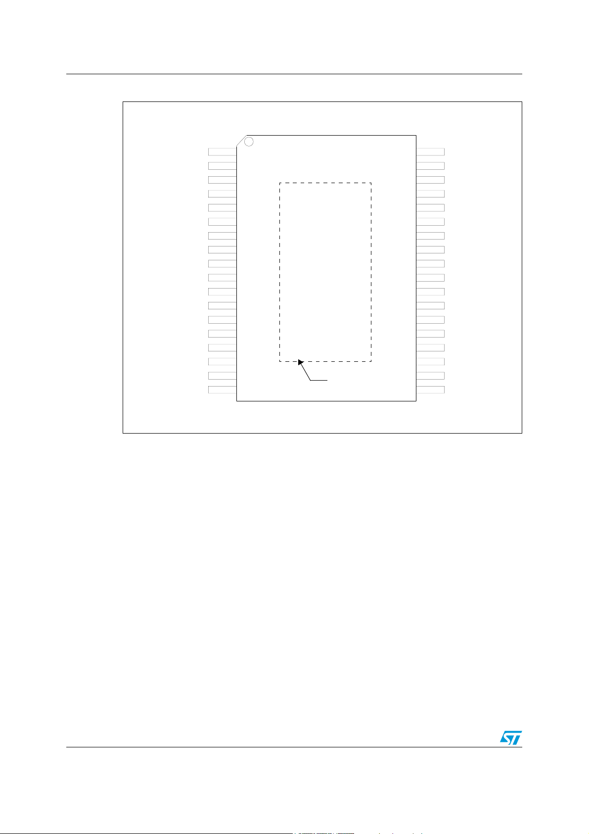
Pin definitions and functions L9952GXP
/
_
Figure 2. Pins configuration
1
Dig
GND
NRESET
OP
OP2 -
OPOUT
CLK
CSN
PWM
PWM
Dig_Out
4
INT _
Out
V 22
V1 3
INH
RxD
TxD
2+
2
DI
DO
1
2
3
10
11
12
13
14
15
16
17
18
PowerSSO-36
4
5
6
7
8
9
L9952
GXP
TA B = G N D
35
33
32
31
30
29
28
27
26
25
24
23
22
21
20
19
FSO 36
REL 2
REL 134
LIN
LINPU
Vs
OUT
HS
OUT 1
OUT 2
OUT 3
OUT 4
OP 1 +
OP 1 -
OPOUT 1
WU 1
WU 2
WU 3
WU 4
10/68 Doc ID 13518 Rev 5
Page 11

L9952GXP Description
2 Description
2.1 Voltage regulator
The L9952GXP contains 2 independent and fully protected low drop voltage regulators,
which are designed for very fast transient response.
The output voltage is stable with loads capacitors >
2.1.1 Voltage regulator: V1
The voltage regulator V1 provides 5V supply voltage and up to 250mA continuous load
current for the external digital logic (micro controller, CAN transceiver ...). In addition the
regulator V1 drives the L9952GXP internal 5V loads. The voltage regulator is protected
against overload and over-temperature. An external reverse current protection has to be
provided by the application circuitry to prevent the output capacitor from being discharged
by negative transients or low input voltage. The output voltage precision is better than +/-2%
(incl. temperature drift and line-/load regulation) for operating mode; respectively +/-3%
during low current mode. Current limitation of the regulator ensures fast charge of external
bypass capacitors. The output voltage is stable for ceramic load capacitors >
If device Temperature exceeds TSD1 threshold, all outputs (Hsx, Lsx, V2, LIN) will be
deactivated except V1. Hence the micro controller has the possibility for interaction or error
logging. In case of exceeding TSD2 threshold (TSD2>TSD1), also V1 will be deactivated
(see state chart Fig. 3.1: “Protection and diagnosis”). A timer is started and the voltage
regulator is deactivated for t
LIN, and WU1...4) are disabled. After 1 sec, the voltage regulator will try to restart
automatically. If TSD2 occurs within one minute and for 8 consecutive times, the L9952GXP
enters the V
In case of short to GND at “V1” after initial turn on (V1 < 2V for at least 4ms) the L9952GXP
enters the V
signals from CAN, LIN, WU1..4, SPI.
- standby mode.
BAT
- standby mode. Reactivation (wake-up) of the device can be achieved with
BAT
220nF.
220nF.
= 1sec. During this time, all other wakeup sources (CAN,
TSD
2.1.2 Voltage regulator: V2
The voltage regulator V2 supplies additional 5V loads (e.g. Logic components, external
sensors, external potentiometers). The continuous load current is 50mA. The regulator
provides accuracy better than +
In case of short to GND at “V2” after initial turn on (V2 < 2V for at least 4ms) the V2
regulator is switched off. Micro processor has to send a clear command to reactivate the V2
regulator.
V2 is protected against:
● Overload
● Over temperature
● Short circuit (short to ground and battery supply voltage)
● Reverse biasing
3% @ 50mA (4% @ 100mA) load current.
Doc ID 13518 Rev 5 11/68
Page 12

Description L9952GXP
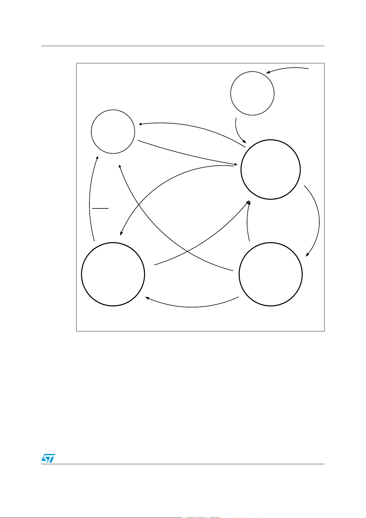
2.2 Power control in operating modes
The L9952GXP can be operated in 4 different operating modes:
● Active
● Flash
● V
● V
A cyclic monitoring of wake-up inputs is available in stand-by modes.
2.2.1 Active mode
All functions are available.
2.2.2 Flash mode
To disable the watchdog feature a FLASH program mode is available.
- standby
1
- standby
BAT
The mode can be entered by V
PWM2
≥ 9V
In this case all other functions are the same as in active mode
Watchdog can be disabled as well as soon as L9952GXP enters the V1 standby mode (see
section 2.9 for details)
Note: “High” level for flash mode selection is V
5V logic signals are required. For proper operation PWM
above standard 5V logic.
2.2.3 V1 standby mode
Outputs and internal loads are switched off. To supply the micro controller in a low power
mode, the voltage regulator1 (V1) remains active. The intention of the V1 standby mode is
to preserve the RAM contents. A cyclic contact supply and wake-up input sense feature (for
cyclic monitoring of external contacts) can be activated by SPI.
2.2.4 V
To achieve minimum current consumption during V
functions (except the ones for wake up functionality) are switched off.
In V
(without cyclic sense feature selected).
The transitions from active mode to either V
SPI.
standby mode
BAT
- standby mode the current consumption of the L9952GXP is reduced to 7µA, typical
BAT
≥ 9V. For all other operation modes, standard
PWM2
1 must not be set to a voltage level
standby mode, all L9952GXP
BAT
-standby or V
1
- standby are controlled by
BAT
V
- standby mode is dominant; i.e. if both bits, V1 - standby and V
BAT
“1”, the L9952GXP will enter V
- standby mode.
BAT
12/68 Doc ID 13518 Rev 5
- standby are set to
BAT
Page 13
L9952GXP Description
2.3 Wake up events
A wake-up from standby mode will switch the device to active mode. This can be initiated by
one or more of the following sources:
● Change of the LIN state at LIN bus interfaces
● A current at the INH pin (I ≥200uA) controlled by the CAN-transceiver (the CAN
transceiver is not a part of the IC).
● Positive/negative edge at wake up pins WU1...WU4 -> change of level after going into
stand-by
● Change of open-load state at OUT1 to 4
● SPI access in V1-standby mode (CSN is low and first rising edge on CLK)
Table 3. Wake up events
Wake up source Description
LIN Always active
INH Always active
WU1...4 Can be individually disabled via SPI
Open Load at HS outputs Can be individually disabled via SPI
SPI Access
High level at PWM2 input VPWM2 > 9V
Always active
(except in V
- standby mode)
BAT
(1)
1. Only if internal oscillator is running (e. g. in cyclic sense configuration or after wake-up request).
All wake-up events (except wake-up by LIN, INH or SPI from V1standby mode) generate a
Reset pulse (NReset low for 2ms).
Wake-up events from V1standby by LIN, INH or SPI do not cause a Reset and the Reset
generation is blocked for 2ms, i. e. a watchdog failure during this timeframe will not cause a
reset.
Doc ID 13518 Rev 5 13/68
Page 14
Description L9952GXP
2.4 Functional overview (truth table)
Table 4. Functional overview (truth table)
Operating modes
-standby
Function Comments
Active mode
V
1
static mode
(cyclic sense)
2.3.1 Voltage-regulator, V1 VOUT= 5V On On
2.3.2 Voltage-regulator, V2 VOUT= 5V On / Off
(2)
On
(2)
(1)
/ Off On
V
-standby
BAT
static mode
(cyclic sense)
Off
(2)
2.3.3 Reset-generator On On Off
Off if
2.3.4 Window watchdog V
monitor On
1
2.3.5 Wake up Off
2.3.6 HS-cyclic supply
Oscillator
timebase
On / Off On
(3)
(I_V1 < I
and I
or I
CMP
Active
(2)
CMP
=0)
CMP
= 1
(4)
/ Off On
Off
Active
(2)
2.3.7 Relay driver On Off Off
2.3.8 Operational amplifiers On Off Off
2.3.9 LIN line driver LIN 2.1 On Off Off
2.3.10 LIN line receiver On On On
Hi – no error
Lo – WD or V1
fail
2.3.11 FSO
Fail-safe
output
2.3.12 Oscillator On
2.3.13 Vs-Monitor On
Hi – no error
Lo – WD or V1
fail
(5)
(6)
(7)
Lo -> because
V1= off
(6)
(7)
/ Off
(4)
/ Off
1. Supply the processor in low current mode
2. Only active when selected via SPI
3. Input Status can be read by SPI (Status Register 0); Inputs should be configured for static sense (Control
Register 2)
4. Unless disabled by SPI
5. Watchdog is active in V1 standby mode, until I(V1) is below I
6. Activation = ON if cyclic sense is selected
7. Cyclic activation = pulsed ON during cyclic sense
14/68 Doc ID 13518 Rev 5
current threshold
CMP
Page 15
L9952GXP Description
Figure 3. Operating modes, main states
Vs > Vpor
Vbat startup
All registers
clear ed to ‚0',
Cold start bit (D19, SR0)
set to ‚ 1'
Vpwm2>9V
Flash Mode
Watchdog: OFF
Vpwm2<7V
Active
Mode
V1: on
Reset Generator: active
Watchdog: active
Fail Safe Out: active
Vpwm2>9V
Note 1
SPI command: ‚Go Vbat’ ( D20 CR0)
V1 fail (V1 < 2,5V for 4ms after POR)
OR
Thermal Shutdown
OR
=> shor t to GN D
Or
15 x WD Fa ilur e
Vbat Standby
Mode
V1: off
V2: according to SPI settings
Reset Generator: off (Nreset=low)
Watchdog: off
Fail S afe Out : low
HSD, LSD: Off
Not e 1: only if internal oscilla tor is runn ing
Vpwm 2>9V
Note 1
Thermal Shutdown TSD2
OR IV1 > 1mA AND ICMP = 0 AND 15 x WD fail
Wake-up
Event
Wake-up
Event
V1 Stan d b y
Mode
V1: on
Reset Generator: active
Watchdog:
OFF (if Iv 1<I
or ICMP = 1)
cmp
Fail Safe Out: active
SPI command: ‚Go Vcc’
(D21 CR0)
Doc ID 13518 Rev 5 15/68
Page 16

Description L9952GXP
2.5 Wake up inputs
The de-bounced digital inputs WU1...WU4 can be used to wake up the L9952GXP from
standby modes. These inputs are sensitive to any level transition (positive and negative
edge)
For static contact monitoring, a filter time of 64 µs is implemented at WU1-4. The filter is
started when the input voltage passes the specified threshold. At Vin > 1V and Vin < (Vs –
2V), a Wake-up request is processed. During Wake-up request, the internal oscillator and
other circuit blocks are activated in order to allow more accurate monitoring of the inputs.
In addition to the continuous sensing (static contact monitoring) at the wake up inputs, a
cyclic wake up feature is implemented. This feature allows periodical activation of the wakeup inputs to read the status of the external contacts. The periodical activation can be linked
to Timer 1 (0.5sec to 4.0sec in 0.5sec steps) or Timer 2 (50ms). The input signal is filtered
with a filter time of 16us after a programmable delay (80us or 800us). A Wake-up will be
processed if the status has changed versus the previous cycle.
The Outputs OUT_HS and OUT1-4 can be used to supply the external contacts with the
timing according to the cyclic monitoring of the wake-up inputs.
If the wake-up inputs are configured for cyclic sense mode (Icxx in control register 2), the
same input filter timing (Timer1 or Timer2) and the corresponding input filter delay (control
register 2) must be used for the HS Outputs (Hsxx in control register 0) which supply the
external contact switches.
In Standby mode, the inputs WU1-4 are SPI configurable for pull-up or pull-down current
source configuration according to the setup of the external contacts (pull-up for active low
contacts, pull-down for active high contacts). In active mode the inputs have a pull down
resistor of 100 kOhm (typ).
In Active mode, the input status can be read by SPI (Status Register 0). Static sense should
be configured (Control Register 2) before the read operation is started (In cyclic sense
configuration, the input status is updated according to the cyclic sense timing; Therefore,
reading the input status in this mode may not reflect the actual status).
2.6 Hall sensor ports: WU3,4, Dig_Out 3,4
Applications like Hall sensor outputs need high processing speed. The 12V signals
connected to the wakeup inputs WU3 and WU4 can be looped through to the digital outputs
Dig_Out 3 and Dig_Out 4 (5V) in order to avoid read out of the input state by SPI.
The setup is programmable by SPI.
The open load states of the High Side Drivers OUT1 and OUT2 can be looped through the
digital outputs Dig_Out3 and Dig_Out4 without delay. In addition, the status of OUT1 and
OUT2 can be accessed through the SPI interface. This feature is intended for 2-pin HALL
sensors. Open Load information is only valid during ON state.
The Open Load threshold at pins OUT1...4 can be switched from I
I
= 8 mA via SPI .
OLD2
16/68 Doc ID 13518 Rev 5
OLD1
= 2mA to
Page 17

L9952GXP Description
2.7 Interrupt
Dig_Out4 can be configured via SPI as Interrupt output (INT) by setting Bit 20 /
CR1:INT_enable=’1’.
This configuration will enable the following behaviour:
● INT pin is pulled high for 2ms in case of any wake-up from V1 standby mode (WU
inputs, LIN, INH, SPI, open load HS, Iv1 > I
● Wake-up events from V1 standby do not generate a reset (i.e. NRESET is not pulled
CMP
_ris)
low)
● The Dig_Out4 settings in CR1 (Bits 12..14) will be ignored
2.8 Cyclic contact supply
In V1 and V
standby mode, any high side driver output (OUT1..4, OUTHS) can be used
BAT -
to periodically supply external contacts.
The timing is selectable by SPI
Timer 1: period is X sec, the on-time is 10ms resp. 20ms
With X ∈ {0.5, 1.0, 1.5, ... 4 }
Timer 2: period is 50ms, the on- time is 100us resp. 1ms:
Note: Cyclic sense setup: if cyclic sense feature is used for wake-up inputs (Icxx in control register
2), same input filter timing (Timer1 or Timer2) must be used for HS Outputs (Hsxx in control
register 0).
2.9 Window – watchdog
During normal operation the watchdog monitors the micro controller within a nominal trigger
cycle of 10ms.
In V
automatically disabled. However, the watchdog will remain enabled in V1-standby mode
until the current at V1 decreases below I
disabled, if the I
After ‘power-on’, ‘standby mode’ or reset, the window watchdog starts with a long open
window (65ms). The long open window allows the micro controller to run its own setup and
then to trigger the watchdog via the SPI. The trigger is finally accepted when the CSN input
becomes HIGH after the transmission of the SPI word.
-standby , V1-standby and Flash program modes, the watchdog circuit is
BAT
_fall. The V1 current monitoring can be
bit (CR2, D20) is set to '1'.
CMP
CMP
A correct watchdog trigger will start the window watchdog with a closed window (< 6ms)
followed by an open window (< 10ms), see timing diagrams. Subsequently, the micro
controller has to serve the watchdog by alternating the watchdog trigger bit (CR0, D19). The
“negative” or “positive” edge has to meet the open window time. A correct watchdog trigger
signal will immediately start the next closed window.
After 8 watchdog failures in sequence, the V1 regulator is switched off for 200ms. In case of
7 further watchdog failures, the V1 regulator is completely turned off and the device goes
into V
standby mode until a wakeup occurs. (e.g. via LIN, CAN/INH).
BAT -
Doc ID 13518 Rev 5 17/68
Page 18
Description L9952GXP
The watchdog is triggered by toggling the trigger bit (CR0, D19).
Note: The active trigger window will be reset after each correct trigger write operation.
In case of reset (NReset low for 2ms) the trigger bit is set to “0”.
In case of a WD failure, the outputs (Lsx, Hsx, V2) are switched off and NReset is pulled low
for 2ms.
Writing to control register 0 without inverting the WD trigger bit is possible at any time.
Figure 4.
(Nreset =low for 2ms)
LSD: Off (control bits set to ‚0')
HSD: Off (control bits remain
Watchdog
t=200ms
Reset
unchanged)
Wake up event
V1 off
for 200 m s
Watchdog Failure
Vbatstdby
Mode
8x WD Failure
Watchdog Failure (‚long
open window’ passed
without TRIG=1
2ms
8+7
WD Failu res
Toggle WD Trigger Bit
Within nominal window
Watchdog active
With
Normal window
(10ms)
HS D, LSD : accor ding to
CR0
Set WD Tr igger Bit = ‚ 1' or
toggle trigger bit if wake-up
from V1standby
Wake- up eve nt
or exit Flash Mode
Go to st and by mod e or
Power-on
Reset
Flash Mode ( PWM2>9V)
Watchdog
Inactive
(standby modes,
Flash Mode)
INH, LIN, SPI
I(V1)>1mA and ICMP=0
18/68 Doc ID 13518 Rev 5
Watchdog active
with
‚long open wi ndow’
(65ms nom )
HS and LS outputs are
off
or F lash Mode (PWM2>9V )
Set
WD Trigger Bit = ‚0' or write
non-inverting value to tr igger
bit after wake-up from
V1 stand by mod e
Go to standby mode
Page 19
L9952GXP Description
2.10 Fail safe output
After power-on (Vs > V
) or wakeup from V
POR
-standby mode, the output FSO is set to
BAT
“HIGH”, if V1 is above the V1 threshold. FSO is set to “LOW” in case of V1 under voltage or
watchdog failure.
During V1-standby mode, FSO is HIGH unless a V1 under-voltage or watchdog reset
occurs. WD remains enabled in V1 standby mode until I
standby mode, FSO is low. At exit from V
- standby mode, it goes to high as soon as V1
BAT
drops below 150uA. In V
V1
BAT
-
is stable.
At wakeup FSO remains high, provided that the watchdog is triggered successfully. It is set
low if the watchdog is not served during the long open window of if a V1 under-voltage
occurs.
Figure 5. FSO
TSD2
V1 undervoltage
Vbatstdby Mode
FSO = 0
Watchdog Failure
2.11 Reset – generator
IF V1 is turned on and the voltage exceeds the V1 reset threshold, the reset output
“NRESET” is switched to “HIGH” after a 2ms reset delay time. This is necessary for a
defined start of the micro controller when the application is switched on.
As soon as an under voltage condition of the output voltage (V1 < VRT) for more than 8us
appears, the reset output is switched low again.
Figure 6. NReset
Wake-up Event 1)
Vpwm2 < 9V
(Exit Flash Mode)
V1 Undervoltage
Watchdog
Failure
NReset = 0
1) Only if
(INT_en = 0) and (wake-up by WU-input or High Side Open Load)
Doc ID 13518 Rev 5 19/68
Page 20

Description L9952GXP
2.12 V1, V2 fail
The V
In case of a drop below the V
and V2 regulator output voltages are monitored.
1,
– fail thresholds (V
1, V2
bits are latched. The fail bits are cleared by a dedicated SPI command.
If 4ms after turn on of the regulator the V
voltage is below the V
1,2
(independent for V1,2 ), the L9952GXP will identify a short circuit condition at the related
regulator output and the regulator will be switched off.
In case of a V1 failure the device enters V
- standby mode automatically.
BAT
In case of a V2 failure the SHT5V2 bit (SR0 Bit12) is set.
2.13 Low side driver outputs Rel1, Rel2
The outputs Rel1, Rel2 (R
loads.
Typical relays used have the following characteristics:
Relay type 1:
– closed armature: R = 160 Ω +
– open armature: R = 160 Ω +
Relay type 2:
– closed armature: R= 220 Ω +
– open armature: R= 220 Ω +
= 2 Ω typ. @25 °C) are specially designed to drive relay
DSon
10%, L= 300mH
10%, L= 240mH
10%, L= 420mH
10%, L= 330mH
< 2V,typ for t > 2us), the V
1,2
fail thresholds,
1,2
1,2
- fail
The outputs provide an active output zener clamping (40V) feature for the demagnetisation
of the relay coil, even though a load dump condition exists. In case of watchdog failure the
relay drivers will be switched off and the low side driver control bits are cleared.
Note: 1 Due to relays bouncing, high dV/dt and/or dI/dt transients may occur on the low side driver
outputs. In case high currents are switched (for example window lift motor), due to parasitic
capacitive inductive coupling from load side of relays to the relays coils, the Absolute
Maximum Ratings of the Low Side driver outputs may be exceeded. In order to avoid this, it
is recommended to place a 10nF capacitor at the Rel1, Rel2 outputs to GND.
2 If a hard short circuit to V
required with T
> 1µs, R ≥ 1 Ω (see block diagram, the value is given for an output short
RC
is possible at the "Low Side Driver" outputs, an RC network is
BAT
circuit of given di/dt = 5A/µs).
2.14 PWM inputs
The inputs PWM 1,2 can be used to control the output drivers Out1..4 and OUT_HS with a
PWM signal. Each PWM input can be mapped individually to each of the above listed
outputs according to the SPI settings.
20/68 Doc ID 13518 Rev 5
Page 21
L9952GXP Description
2.15 Operational amplifiers
The operational amplifiers are especially designed to be used for sensing and amplifying the
voltage drop across ground connected shunt resistors. Therefore the input common mode
range includes - 0.2 ... 3V.
The operational amplifiers are designed for GND + 3V... GND – 0.2V input voltage swing
and rail-to-rail output voltage range. All Pins (positive, negative and outputs ) are available
to be able to operate in non-inverting and inverting mode. Both operational amplifiers are
on-chip compensated for stability over the whole operating range within the defined load
impedance.
Figure 7. Lin master pull up
Vs
LIN
control
T
SW
control
LIN PU
A dedicated built-in switch “Tsw” enables the LIN to act as a master. (see chapter
2.16 LIN bus interface
General requirements:
● Speed communication up to 20kbit/s
● LIN 2.0 compliant (SAEJ2602 compatible) transceiver
● Function range from +40V to -18V DC at LIN Pin
● GND disconnection fail safe at module level
● Off mode: does not disturb network
● GND shift operation at system level
● Microcontroller Interface with CMOS compatible I/O pins.
● Pull up resistor internal.
● ESD: immunity against automotive transients per ISO7637 specification (see
application note)
● Matched output slopes and propagation delay
In order to further reduce the current consumption in standby mode, the integrated LIN bus
interface offers an ultra low current consumption.
30k
Gnd
LIN
Master node
1k
pull up
2.18)
Doc ID 13518 Rev 5 21/68
Page 22

Description L9952GXP
2.17 Error handling
The L9952GXP provides the following 3 error handling features which are not described in
the LIN Spec. V2.1, but are realized in different stand alone LIN transceivers / micro
controllers to switch the application back to normal operation mode.
2.17.1 Dominant TxD time out
If TXI is in dominant state (low) for more than 12ms (typ) the transmitter will be disabled until
TXI becomes recessive (high). This feature can be disabled via SPI.
2.17.2 Short to battery time out
If TXI changes to dominant (low) state but RXI signal does not follow within 40µs, the
transmitter will be disabled until TXI becomes recessive (high).
2.17.3 Short to ground mode
A wake up caused by a message on the bus will start the voltage regulator and the micro
controller to switch the application back to normal operation mode.
2.18 Wake up (from LIN)
In standby mode the L9952GXP can receive a wake up from LIN bus. For the wake up
feature the L9952GXP logic differentiates two different conditions.
2.18.1 Normal wake up
Normal wake up can occur when the LIN transceiver was set in standby mode while LIN was
in recessive (high) state. A dominant level at LIN for at least 40µs, will switch the L9952GXP
to active mode.
2.18.2 Wake up from short to GND condition
If the LIN transceiver was set in standby mode while LIN was in dominant (low) state,
recessive level at LIN for at least 40us, will switch the L9952GXP to active mode.
2.18.3 RxD pin in V1 standby
In V1 standby condition the RxD is a tristate pin.
22/68 Doc ID 13518 Rev 5
Page 23

L9952GXP Description
2.19 LINPU
The LINPU (LIN pull up) signal is set by L9952GXP logic in order to drive the LIN transceiver
in master mode. The master mode is realized by an internal high side switch and an external
diode in series with an external 1k resistor. In master mode the high side switch is closed
causing an external pull up path in parallel to the internal one (diode & 30k resistor).
HS (high side) characteristics:
● HS does not have an over current protection.
● The HS remains active in standby mode.
● Switch off only in case of over temperature (TSD2 = thermal shutdown #2).
● Typical R
DSon
, 10 Ω.
The Linpu is activated by default (LIN master mode) and can be switched off with a SPI
command (see register 2) to reduce current in case of LIN shorted to ground.
2.20 Serial Peripheral Interface (SPI)
A 24 bit SPI command (2 adresses + 22 data bits) is used for bi-directional communication
with the micro controller.
During active mode, the SPI:
1) triggers the watchdog
2) controls the modes and status of all L9952GXP modules (incl. input and output drivers)
3) provides driver output diagnostic
4) provide L9952 diagnostic (incl. over temperature warning, L9952GXP operation status)
Note: During stand-by modes, the SPI is generally deactivated.
The SPI can be driven by a micro controller with its SPI peripheral running in following
mode:
CPOL=0 and CPHA=0.
For this mode input data is sampled by the low to high transition of the clock CLK, and
output data is changed from the high to low transition of CLK.
This device is not limited to micro controller with a build-in SPI. Only three CMOScompatible output pins and one input pin will be needed to communicate with the device. A
fault condition can be detected by setting CSN to low. If CSN = 0, the DO-pin will reflect the
global error flag (fault condition) of the device which is a logical -”OR” of all over current, Vsover / under voltage, temperature warning/shutdown and V1 Fail bits. The micro controller
can poll the status of the device without the need of a full SPI-communication cycle.
2.20.1 Chip Select Not (CSN)
The input pin is used to select the serial interface of this device. When CSN is high, the
output pin (DO) will be in high impedance state. A low signal activates the output driver and
a serial communication can be started. The state during CSN = 0 is called a communication
frame.
Doc ID 13518 Rev 5 23/68
Page 24

Description L9952GXP
2.20.2 Serial Data In (DI)
The input pin is used to transfer data serial into the device. The data applied to the DI will be
sampled at the rising edge of the CLK signal and shifted into an internal 24 bit shift register.
At the rising edge of the CSN signal the contents of the shift register will be transferred to
Data Input Register. The writing to the selected Data Input Register is only enabled if exactly
24 bits are transmitted within one communication frame (i.e. CSN low). If more or less clock
pulses are counted within one frame the complete frame will be ignored. This safety
function is implemented to avoid an activation of the output stages by a wrong
communication frame.
Note: Due to this safety functionality a daisy chaining of SPI is not possible. Instead, a parallel
operation of the SPI bus by controlling the CSN signal of the connected IC's is
recommended.
2.20.3 Serial Data Out (DO)
The data output driver is activated by a logical low level at the CSN input and will go from
high impedance to a low or high level depending on the global error flag (fault condition).
The first rising edge of the CLK input after a high to low transition of the CSN pin will transfer
the content of the selected status register into the data out shift register. Each subsequent
falling edge of the CLK will shift the next bit out.
2.20.4 Serial Clock (CLK)
The CLK input is used to synchronize the input and output serial bit streams. The data input
(DI) is sampled at the rising edge of the CLK and the data output (DO) will change with the
falling edge of the CLK signal. The SPI can be driven with a CLK frequency up to 1MHz.
2.20.5 Data registers
The device has 3 Control registers and 2 Status registers. The first two bits (D22+D23) at
the DI-Input are used to select one of the Control registers. All bits are first shifted into an
input shift register. After the rising edge of CSN the contents of the input shift register will be
written to the selected Control register only if a frame of exact 24 bits is detected. If the
Control register 1 is selected for data transfer, the Status register 1 will be transferred to the
DO during the current communication frame. For the selection of Control register 0 or
Control register 2, the Status register 0 is transferred to DO.
24/68 Doc ID 13518 Rev 5
Page 25

L9952GXP Protection and diagnosis
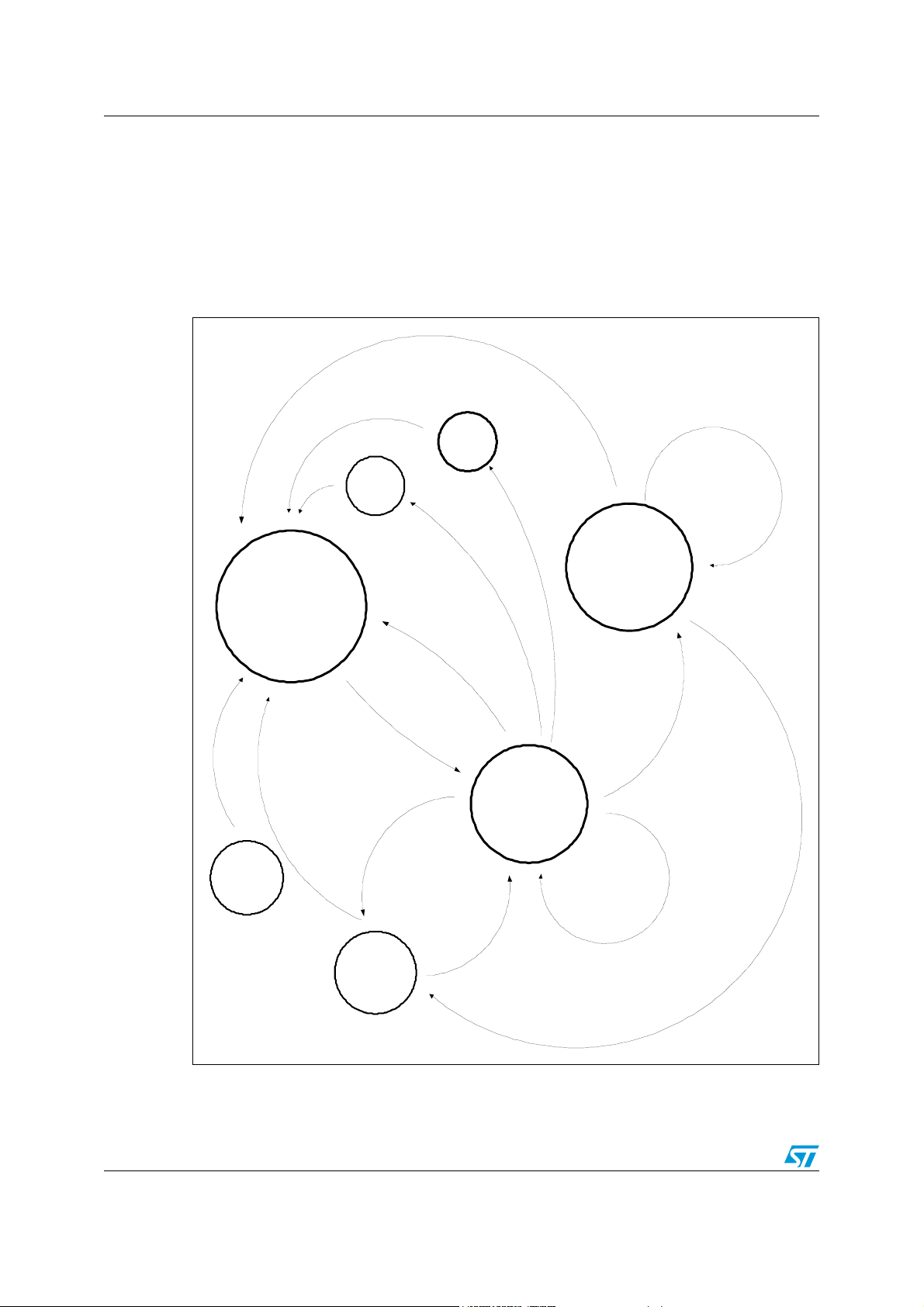
3 Protection and diagnosis
3.1 Power supply fail
Over and under-voltage detection on Vs.
3.1.1 Over voltage
If the supply voltage Vs reaches the over voltage threshold (V
● The outputs HS1..4, OUT_HS, Rel1,2, and LIN are switched to high impedance state
(load protection)
● The over voltage bit is set and can be cleared with the clear bit (CR1,CLR)
● Automatic recovery after Vs over-voltage; selectable via SPI (CR2, bit4)
3.1.2 Under voltage
If the supply voltage Vs drops below the under voltage threshold voltage(V
● The outputs HS1..4, OUTHS, Rel1,2, and LIN are switched to high impedance state
(load protection)
● The under voltage bit is set
● Automatic recovery after Vs under-voltage; selectable via SPI (CR2, bit4)
3.2 Temperature warning and thermal shutdown
See state chart: “ Protection and diagnosis”.
3.3 SPI diagnosis
Digital diagnosis features are provided by SPI:
● V1 reset threshold programmable
● Over temperature including pre warning
● Open load separately for each output stage
● Overload status
● Vs-supply over/under voltage
● V1 and V2 fail bit
● Status of the WU1...4, LIN and INH pin
● Cold start bit
● Number of unsuccessful V1 restarts after thermal shutdown
● Number of sequential watchdog failures
● Status of watchdog trigger bit TRIG: (SR1, Bit 16)
● LIN status (short to ground, short to V
, dominant TxD)
BAT
See the following state chart: “Protection and diagnosis”.
SOV
)
)
SUV
Doc ID 13518 Rev 5 25/68
Page 26

Protection and diagnosis L9952GXP
Figure 8. Protection and diagnosis
Tj > 155°C
>
T
SPI command: ‚CLR’
(D21 CR1)
Power- on reset
Active
Mode
Standb y Modes
SPI command: ‚CLR’
Autorestart activated
1
e
s
c
OR
SPI command: ‚CLR’
(D21 CR1)
OR
Power-on r eset
(D21 CR1)
OR
(D4 CR2)
TSD1
All outputs except V 1: off
‚TS D 1' -Bit is set (D 3 SR1 )
Tj > 140°C
Temperature
Warning
‚Te mper atu re Wa rnin g' -
Bit set
(D2 S R1)
Tj > 130°C
Vs Undervolt age
8x TSD2
(each TSD2
within 1 min)
Vbatstdby
All outputs incl V2: off
Power- on reset
Vs Overvoltage
TSD2
All outputs: off
V1: off for 1 sec
‚TSD2-bit is set (D4 SR1)
Wake-up event
SPI command: ‚CLR’
(D21 CR1)
Autorestart activated
(D4 CR2)
(during cyclic sense)
OR
Vs Lockout
All outputs : high Impedance
OV Bit set (D0 SR1)
Auto-restart if selected by SPI
8 successive watchdog
26/68 Doc ID 13518 Rev 5
failures
V1 off for
200m s
Vs Lockout
All outputs: off
UV bit set (D1 SR1)
Auto -resta rt if sele cted by SPI
7 additional watchdog failures
in sequence
Vbatstdby
mode
Page 27

L9952GXP Protection and diagnosis
3.4 High side driver outputs
The component provides a total of 4 high side outputs Out1...4, (7 Ω typ. @ 25C) to drive
e.g. LED' s or hall sensors and 1 high side output OUT_HS with 1 Ω typ. @ 25 C).
The high side outputs are protected against
● Over- and under voltage
● Overload (short circuit)
● Over temperature with pre warning
If the output current exceeds the current shutdown threshold the output transistor is turned
off and the corresponding diagnosis bit of the output is set.
The switches are automatically disabled in case of reset condition, Vs-under, Vs-over
voltage or thermal shutdown (TSD1&2).
For OUT_HS an auto recovery feature is available in active mode.
If the OUT_HS output current exceeds the current shutdown threshold, the output transistor
is turned off and the corresponding diagnosis bit of the output is set.
Via SPI command the auto recovery feature can be enabled in order to restart the driver in
case of over current shutdown. This over current recovery feature is intended for loads
which have an initial current higher than the over current limit of the output (e.g. Inrush
current of cold light bulbs).
The device itself can not distinguish between a real overload and a non linear load like a
light bulb. A real overload condition can only be qualified by time. As an example, the micro
controller can switch on light bulbs by setting the over current recovery bit for the first 50ms.
After clearing the recovery bit, the output will be automatically disabled if the overload
condition still exists.
The status of all high side outputs (over-current, open load) can be monitored by SPI
interface.
In case of a watchdog failure, the high side drivers are switched off. The control bits are not
cleared, i.e. the drivers will go to the previous state once the watchdog failure condition
disappears.
ESD structures are configured for nominal currents only. If external loads are connected to
different grounds, the current load must be limited to this nominal current.
Note: Loss of ground or ground shift with externally grounded loads.
3.5 Low side driver outputs Rel1, Rel2
The outputs provide an active output zener clamping feature for the demagnetisation of the
relay coil, even though a load dump condition exists. For safety reasons the relay drivers
are linked with the Watchdog: in case of failure, or missing trigger signal the relay drivers will
switch off.
Doc ID 13518 Rev 5 27/68
Page 28

Absolute maximum ratings L9952GXP
4 Absolute maximum ratings
Table 5. Absolute maximum ratings
Symbol Parameter Value Unit
V
S
V
1
V
2
V
DI VCLK
V
TXD VCSN
V
DO VRXD
V
NRESET VFSO
V
DIGOUT3,4
V
INH
V
PWM1, VPWM2,
V
REL1, VREL2,
V
OUT1..4,, VOUTH
V
WU1...4,
V
OP1+,VOP1-,
V
OP2+, VOP2-,
V
OPOUT1,
V
OPOUT2
V
LIN, VLINPU
I
Input
DC supply voltage / “jump start” -0.3 to +28 V
Single pulse / t
“transient load dump”
Stabilized supply voltage, logic
supply
< 400 ms
max
-0.3 to +40 V
-0.3 to +5.25 V
Stabilized supply voltage -0.3 to +28 V
Logic input / output voltage range -0.3 to V1+0.3 V
Wake up input voltage range
PWM input voltage range
-0.3 to +40 V
Low side output voltage range
High side output voltage range -0.3 to VS + 0.3 V
Wake up input voltage range -0.3 to VS + 0.3 V
Opamp1 input voltage range
Opamp2 input voltage range
-0.3 to V1 + 0.3 V
Analog Output voltage range -0.3 to VS + 0.3 V
LIN bus I/O voltage range -20 to +40 V
Current injection into Vs related
input pins
5mA
Note: All maximum ratings are absolute ratings. Leaving the limitation of any of these values may
cause an irreversible damage of the integrated circuit !
28/68 Doc ID 13518 Rev 5
Page 29

L9952GXP ESD protection
5 ESD protection
Table 6. ESD protection
Parameter Value Unit
(2)
(1)
+/- 2 kV
+/- 4 kV
+/- 1.5 kV
+/- 8 kV
All pins, except LIN
All output pins
(3)
LIN
(4)
LIN
All pins (charge device model)
Corner pins (charge device model)
(5)
All pins
+/- 500 V
+/- 750 V
+/- 200 V
1. HBM (human body model, 100pF, 1.5 kΩ ) according to MIL 883C, Method 3015.7 or EIA/JESD22A114-A
2. HBM with all none zapped pins grounded
3. Without external components
4. Acc. DIN EN61000-4-2 (330Ω, 150pF), with external components:
- Diode, type ESDLIN1524BJ
- SMD Ferrite bead, type TDKMMZ2012Y202B
- Capacitor C=220pF
For detailed information please see EMC report from IBEE Zwickau (available on request)
5. Acc. Machine Model: C=220pF; L=0.75µH; R=10Ω
Doc ID 13518 Rev 5 29/68
Page 30

Thermal data L9952GXP
6 Thermal data
6.1 Operating junction temperature
Table 7. Operating junction temperature
Item Symbol Parameter Value Unit
6.1.1 Tj Operating junction temperature - 40 to 150 °C
6.1.2 RthjA Thermal resistance junction- ambient See Figure 10. °C/W
6.2 Temperature warning and thermal shutdown
Table 8. Temperature warning and thermal shutdown
Item Symbol Parameter Min. Typ. Max. Unit
6.2.1 T
6.2.2 T
6.2.3 T
6.2.4 T
6.2.5 T
1. Non-overlapping
W ON
SD1 OFF
SD2OFF
SD2 ON
SD12hys
Thermal over temperature
warning threshold
Thermal shutdown
junction temperature 1
Thermal shutdown
junction temperature 2
(1)
T
j
(1)
T
j
(1)
T
j
120 130 140 °C
130 140 150 °C
140 155 170 °C
Hysteresis 5 °C
30/68 Doc ID 13518 Rev 5
Page 31

L9952GXP Thermal data
6.3 Package and PCB thermal data
Figure 9. PowerSSO-36 PC board
Note: Layout condition of Rth and Zth measurements ( board finish thickness 1.6 mm +/- 10%
board double layer, board dimension 129x60, board Material FR4, Cu thickness 0.070mm
(front and back side), thermal vias separation 1.2 mm, thermal via diameter 0.3 mm +/- 0.08
mm, Cu thickness on vias 0.025 mm ).
Doc ID 13518 Rev 5 31/68
Page 32

Thermal data L9952GXP
Figure 10. PowerSSO-36 thermal resistance junction ambient Vs. PCB copper area
(V1 ON)
RTHj _amb(°C/ W)
110
90
70
50
30
0246810
PCB Cu heatsink area (cm^ 2)
Figure 11. PowerSSO-36 thermal impedance junction ambient single pulse (V1 ON)
ZTH (° C/ W)
1000
Footprint
100
2 cm
8 cm
2
2
10
1
0,1
0,01 0,1 1 10 100 1000
Time ( s)
32/68 Doc ID 13518 Rev 5
Page 33

L9952GXP Thermal data
Equation 1: pulse calculation formula
Z
THδ
where δ = t
R
P
TH
/T
δ Z
THtp
1 δ–()+⋅=
Figure 12. PowerSSO-36 thermal fitting model (V1 ON)
Table 9. Thermal parameters
Area/island (cm2)Footprint28
R1 (°C/W) 5
R2 (°C/W) 18 10 10
R3 (°C/W) 29 22 7,8
R4 (°C/W) 51 29 21
C1 (W.s/°C) 0,0003
C2 (W.s/°C) 0,35 1 1
C3 (W.s/°C) 1,5 1,3 1,3
C4 (W.s/°C) 5 15 15
Doc ID 13518 Rev 5 33/68
Page 34

Electrical characteristics L9952GXP
7 Electrical characteristics
7.1 Supply and supply monitoring
The voltages are referred to ground and currents are assumed positive, when the current
flows into the pin. 6V <
unless otherwise specified.
Table 10. Supply and supply monitoring
Item Symbol Parameter Test condition Min. Typ. Max. Unit
V
< 18V; 4.8V < V1 < 5.2V; all outputs open; Tj = -40°C...130°C,
S
7.1.1 V
7.1.2 V
7.1.3 V
7.1.4 V
7.1.5 V
7.1.6 I
7.1.7 I
7.1.8 I
V(BAT)CS
7.1.9 I
7.1.10 I
7.1.11 I
V(BATWU)
V(V1WU)
S
SUV
hyst_UV
SOV
hyst_OV
V(act)
V(BAT)
V(V1)
Supply voltage range 6 13.5 18 V
V
increasing /
VS UV-threshold voltage
S
decreasing
5.11 5.81 V
Undervoltage hysteresis 0.04 0.1 0.15 V
VS OV-threshold voltage
S
decreasing
18 22 V
increasing /
V
Overvoltage hysteresis Hysteresis 0.5 1 1.5 V
Vs=12V, TxD LIN
Current concumption in
active mode
high, V2 on,
Outputs off
2.7 20 mA
Iv1=Iv2=0A
VS=12V, both
Current consumption in
V
- standby mode
BAT
voltage regulators
deactivated, no
1 7 10 µA
wake-up request
V
=12V, both
Current consumption in
- standby mode
V
BAT
S
voltage regulators
deactivated, (cyclic
40 75 100 µA
sense)
V1=5V, VS=12V,
Current consumption in
-standby mode
V
1
Voltage regulator
V1 active, without
cyclic sense, no
10 45 70 µA
wake-up request
Current consumption in
-standby mode with a
V
BAT
1.5V<VWU<(Vs-3V) 220 320 µA
pending wake up request
Current consumption in
V1- standby mode with a
1.5V<VWU<(Vs-3V) 300 410 µA
pending wake up request
34/68 Doc ID 13518 Rev 5
Page 35

L9952GXP Electrical characteristics
7.2 Oscillator
6V < V
Table 11. Oscillator
< 18V; all outputs open; Tj = -40°C...130°C, unless otherwise specified.
S
Item Symbol Parameter Test condition Min. Typ. Max. Unit
7.2.1 F
CLK
Oscillation frequency Vs = 6V...18V
7.3 Power-on reset (Vs)
All outputs open; Tj = - 40°C...130 °C, unless otherwise specified.
Table 12. Power-on Reset (Vs)
Item Symbol Parameter Test condition Min. Typ. Max. Unit
7.3.1 V
7.3.2 V
THUP_POR
Hys_POR
V
POR
7.4 Voltage regulator V1
The voltages are referred to ground and currents are assumed positive, when the current
flows into the pin. 5.25V <
Table 13. Voltage regulator V1
V
S
0.808
1.01 1.35 MHz
threshold 2.8 3.45 4.1 V
Hysteresis 200 mV
< 27V; Tj = -40°C...130°C, unless otherwise specified.
Item Symbol Parameter Test condition Min. Typ. Max. Unit
7.4.1 V1 Output voltage 5.0 V
I
= 1mA...
7.4.2 V1
7.4.3 Vhc1
7.4.4 VSTB1
7.4.5 VDP1
7.4.6 ICC1
Output voltage tolerance
Active mode
Output voltage tolerance
Active mode, high current
Output voltage tolerance
in low current mode
Drop-out voltage in
undervoltage conditions
Output current in active
mode
LOAD
100mA,
VS = 13.5V
I
= 100mA ...
LOAD
250mA,
VS = 13.5V
I
= 250mA
LOAD
VS = 13.5V,
>80°C
T
j
0mA< I
LOAD<ICMP
VS = 13.5V
I
= 50mA,
LOAD
VS = 4.5V
= 100mA,
I
LOAD
=4.5V
V
S
Max. continuous
load current
+/- 2 %
+/- 3 %
+/- 4 %
0.2
0.3
+/- 4 %
0.4
0.5V V
250 mA
Doc ID 13518 Rev 5 35/68
Page 36

Electrical characteristics L9952GXP
Table 13. Voltage regulator V1 (continued)
Item Symbol Parameter Test condition Min. Typ. Max. Unit
7.4.7 ICCmax1
Short circuit output
current
7.4.8 Cload1 Load capacitor1 Ceramic
7.4.9 tTSD
7.4.10 I
7.4.11 I
7.4.12 I
CMP_ris
CMP_fal
CMP
_hys Current comp. hysteresis 0.5 mA
V1 deactivation time after
thermal shutdown
Current comp. rising
threshold
Current comp. falling
threshold
7.4.13 V1fail V1 fail threshold V1 forced 2 V
1. Placement close to the PAD
7.5 Voltage regulator V2
The voltages are referred to ground and currents are assumed positive, when the current
flows into the pin. 5.25V <
Table 14. Voltage regulator V2
Item Symbol Parameter Test condition Min. Typ. Max. Unit
V
S
Current limitation 400 600 950 mA
(1)
0.22 µF
1 s
Rising current 0.9 2.5 4 mA
Falling current
Tj= -40°C...130°C
Tj= 25°C...130°C
0.75
0.85
1.95
1.95
< 27V; Tj = -40°C...130°C, unless otherwise specified.
mA
7.5.1 V
7.5.2 V
7.5.3 V
7.5.4 V
7.5.5 V
7.5.6 I
7.5.7 I
7.5.8 C
7.5.9 V2
1. Placement close to the PAD
2
2
hc1
STB2
DP2
CC2
CCmax2
load
fail
Output voltage 5.0 V
Output voltage tolerance
Active mode
Output voltage tolerance
Active mode, high current
Output voltage tolerance in
low current mode
Drop-out voltage
Output current in Active
mode
I
= 1mA ...
LOAD
50mA, V
I
LOAD
= 13.5V
S
= 50mA ...
100mA, VS = 13,5V
I
= 0uA ...1mA
LOAD
V
= 13,5V
S
I
= 25mA,
LOAD
= 5 V
V
S
= 50mA,
I
LOAD
= 5 V
V
S
Max. continuous
load current
0,3
0.4
+/- 3 %
+/- 4 %
+/- 5 %
0,4
0.7 VV
100 mA
Short circuit output current Current limitation 200 300 500 mA
Load capacitor Ceramic
(1)
0.22 µF
V2 fail threshold V2 forced 2 V
36/68 Doc ID 13518 Rev 5
Page 37

L9952GXP Electrical characteristics
7.6 Reset generator (V1 supervision)
The voltages are referred to GND and currents are assumed positive, when the current
flows into the pin. 5.25V < V
Table 15. Reset generator
Item Symbol Parameter Test condition Min. Typ. Max. Unit
= 18V; Tj = -40 to 130 °C, unless otherwise specified.
S
7.6.1 V
7.6.2 V
7.6.3 V
7.6.4 R
7.6.5 t
RT1
RT2
RESET
RESET
RR
7.6.6 V1 under-voltage filter time 16 µs
7.7 Watchdog
6V < VS < 18V; 4.8V < V1 < 5.2V; Tj = -40 to 130 °C, unless otherwise specified
Table 16. Watchdog
Item Symbol Parameter Test condition Min. Typ. Max. Unit
7.7.1 t
7.7.2 t
7.7.3 t
7.7.4 t
1. See Figure 13.
LW
CW
OW
WDR
Reset threshold voltage1
Reset threshold voltage2
Reset pin low output
voltage
V
V
I
inc. /
S, VV1
decreasing
inc. /
S, VV1
decreasing
V1 > 1V,
= 1mA
RESET
4.5 4.63 4.75 V
4.25 4.37 4.5 V
0,2 0,4 V
Reset pull up int. resistor 60 110 204 kΩ
Reset reaction time @Iload = 1mA 6 40 µs
(1)
Long open window 48,75 65 81,25 ms
Closed window 4.5 6 7.5 ms
Open window 7.5 10 12.5 ms
Watchdog reset pulse time 1.5 2 2. 5 ms
Doc ID 13518 Rev 5 37/68
Page 38

Electrical characteristics L9952GXP
Figure 13. Watchdog timing
Normal startup operation and timeout failures
WDtrigger
NRESOut
0
Missing uC trigger signal
= correct trigger timing
= early trig ger timin g
= missin g trigg er
TCW+ T
OW
T
LW
normal operation m issing
TCW+ T
OW
trigger
TLW= long window < 65ms
T
= closed window < 6ms
CW
T
= open window < 10ms
OW
T
= watchdog reset = 2ms
WDR
T
CW
trigger signal
time / ms
time / ms
WDR
early
write
T
LW
T
LW
T
WDR
T
WDtrigger
T
LW
T
LW
T
LW
time / ms
NRESOut
0
T
WDR
T
WDR
T
WDR
time / ms
38/68 Doc ID 13518 Rev 5
Page 39

L9952GXP Electrical characteristics
Figure 14. Watchdog, closed and open window tolerances and save trigger area
TWD= 10ms
TWD = nominal trigger time
TCW = closed window
TOW = open window
TCW, max
TCW, min
watchdog failure
4.5
7.8 High side outputs
7.8.1 Output (Out_HS)
The voltages are referred to gnd and currents are assumed positive, when the current flows
into the pin. 6V <
specified.
Table 17. High side outputs (Out_HS)
VS < 18V; 4.8V < V1 < 5.2V; Tj = -40°C...130°C, unless otherwise
TOW, max
TOW, min
save trigger area
undefined
7.5 12 20
undefined
time / ms
Item Symbol Parameter Test condition Min. Typ. Max. Unit
7.8.1
OUT_HS
7.8.2 td
7.8.3 td
7.8.4 td
7.8.5 td
R
DSON
ONHS
OFFHS
SDHS
ARHS
Static Drain Source
On-resistance to supply
(IOUT_HS=150mA)
Switch on delay time 0.2 VS 10 35 60 µs
Switch off delay time 0.8VS 40 95 150 µs
Short circuit filter time
Auto recovery filter time
Tj = 25°C 0 1.0 1.5 Ω
Tj = 125°C 01.63 Ω
Tested by scan
chain
Tested by scan
chain
64*
T
OSC
400*
T
OSC
7.8.6 dVout/dt Slew rate 0.2 0.5 0.8 V/µs
7.8.7 I
7.8.8 I
OSDHS
OLD
Short circuit shutdown
current
Open load detection
current
480 900 1320 mA
40 80 120 mA
Doc ID 13518 Rev 5 39/68
Page 40

Electrical characteristics L9952GXP
7.8.2 Outputs (OUT1...4)
The voltages are referred to GND and currents are assumed positive, when the current
flows into the pin. 6V <
specified.
Table 18. High side outputs (OUT 1..4)
Item Symbol Parameter Test condition Min. Typ. Max. Unit
7.8.11 R
7.8.12 I
DSON
OUT
VS < 18V; 4.8V < V1 < 5.2V; Tj = -40°C...130°C, unless otherwise
= 60mA @
I
On – resistance
Short circuit shutdown
current
LOAD
Tj=+25°C
0712Ω
8V < Vs < 16V 140 235 330 mA
7.8.13 I
7.8.14 I
OLD1
OLD2
7.8.15 SR Slew rate 0.2 0.5 0.8 V/µs
7.8.16 t
7.8.17 t
7.8.18 t
7.8.19 I
1. Parameter guaranteed by design
dONHS
dOFFHS
SCF
(1)
FW
7.9 Relay drivers
The voltages are referred to GND and currents are assumed positive, when the current
flows into the pin. 6V <
specified.
Table 19. Relay drivers
Item Symbol Parameter Test condition Min. Typ. Max. Unit
Open load detection
current 1
Open load detection
current 2
Switch ON delay time 0.2 V
Switch OFF delay time 0.8 V
Short circuit filter time
Loss of GND current
(ESD structure)
Selectable via SPI 0.8 2 4 mA
6813mA
S
S
Tested by scan
chain
10 35 60 µs
40 95 150 µs
64*
T
OSC
100 mA
VS < 18V; 4.8V < V1 < 5.2V; Tj = -40 to 130 °C, unless otherwise
7.9.1 R
7.9.2 I
7.9.3 V
7.9.4 t
7.9.5 t
DSON
OUT
Z
ONHL
OFFLH
DC output resistance
Short circuit shutdown
current
Output clamp voltage
Turn on delay time to 10%
V
OUT
Turn off delay time to 90%
V
OUT
40/68 Doc ID 13518 Rev 5
ILOAD = 100mA @
Tj = +25°C
023Ω
8V < Vs < 16V 250 375 500 mA
(1)
I
= 100mA 40 48 V
LOAD
5 50 100 µs
5 50 100 µs
Page 41

L9952GXP Electrical characteristics
Table 19. Relay drivers (continued)
Item Symbol Parameter Test condition Min. Typ. Max. Unit
7.9.6 t
SCF
Short circuit filter time
7.9.7 SR Slew Rate 0.2 2 4 V/µs
1. The output is capable to switch off relay coils with the impedance of RL=160Ω; L = 300mH
(RL=220Ω; L= 420mH); at V
= 40V (Load dump condition)
S
7.10 Wake up inputs ( WU1..WU4)
The voltages are referred to GND and currents are assumed positive, when the current
flows into the pin. 6V <
Table 20. Wake up inputs
Item Symbol Parameter Test condition Min. Typ. Max. Unit
7.10.1 V
7.10.2 V
7.10.3 V
7.10.4 t
7.10.5 I
7.10.6 R
7.10.7 Nn Number of samples
WUthp
WUthn
HYST
WU
WU_stdby
WU_act
VS < 18V; Tj = -40 to 130 °C, unless otherwise specified.
(1)
(WU1...WU4)
Wake-up negative
edge threshold voltage
Wake-up positive edge
threshold voltage
Hysteresis 0.05 Vs 0.1 Vs 0.15 Vs V
Minimum time for
wake-up
Input current in standby
mode
Input resistor to GND in
active mode and in
standby mode during
wake-up request
1.5V<V
During OUT_HS
on, cyclic sense
mode (100us
cyclic HS on time)
T
64*
OSC
Tested by scan
chain
0.4 Vs 0.45 Vs 0.5 Vs V
0.5 Vs 0.55 Vs 0.6 Vs V
51 64 77 µs
< (Vs-3V) 10 20 30 µA
IN
100 275 450 kΩ
2 (at 80µs and 100µs)
7.10.8 V
7.10.9 V
wuthl
wuthh
Pending wake up
request low threshold
Pending wake up
request high threshold
1.0 1.25 1.5 V
Vs-3 Vs-2.2 Vs-1.4 V
1. Defines whether the inputs W1..4 are configured with current source or current sink in standby mode.
Doc ID 13518 Rev 5 41/68
Page 42

Electrical characteristics L9952GXP
7.11 Wake up input (INH)
The voltages are referred to GND and currents are assumed positive, when the current
flows into the pin. 6V <
Table 21. Wake up input (INH)
Item Symbol Parameter Test condition Min. Typ. Max. Unit
VS < 18V; Tj = -40 to 130 °C, unless otherwise specified.
7.11.1 I
7.11.2 I
7.11.3 I
7.11.4 t
7.11.5 Nn Number of samples
7.12 LIN
Compatible to Lin 2.1 for Baud rates up to 20 kBit/s
The voltages are referred to GND and currents are assumed positive, when the current
flows into the pin.
6V <
Table 22. LIN receiver
Item
LIN LIN receiver
INHth
INHUth
INHhys
WU
Wake-up activate
threshold current
Wake-up passive
threshold current
Wake-up current
hysteresis
Minimum time for wake-up 51 64 77 µs
30 75 120 µA
30 70 120 µA
10 20 µA
During OUT_HS
on, cyclic sense
mode (100µs cyclic
2 (at 80us and
100us)
HS on time)
VS < 18V; 4.8V < V1 < 5.2V; Tj = -40°C...130°C, unless otherwise specified.
Parameter
Symbol
Test condition Min. Typ. Max. Unit
7.12.1 V
7.12.2 V
7.12.3 V
7.12.4 I
7.12.5 I
7.12.6 V
TXDLOW
TXDHIGH
TXDHYS
TXDPU
TXDPD
RXDLOW
Input voltage
dominant level
Input voltage
recessive level
V
TXDHIGH
V
TXDLOW
-
TXD pull up
current
TXD pull-down
current
Output voltage
dominant level
42/68 Doc ID 13518 Rev 5
Normal mode, V1=5V 1 1.3 V
Normal mode, V1=5V 2.2 2.5 V
Normal mode, V1=5V 0.5 0.8 V
Normal and
V1-standby mode ,
-5 -30 -60 µA
V1=5V
V
- standby mode,
BAT
V
TXDHIGH
53060µA
V1=5V
Normal mode, V1=5V,
2mA
0.2 1.5 V
Page 43

L9952GXP Electrical characteristics
Table 22. LIN receiver (continued)
Item
Parameter
Symbol
LIN LIN receiver
7.12.7 V
RXDHIGH
Output voltage
recessive level
Receiver threshold
7.12.8 V
THdom
voltage recessive
to dominant state
Receiver threshold
7.12.9 V
THrec
voltage dominant
to recessive state
7.12.10 V
7.12.11 V
7.12.12 V
7.12.13 V
THhys
THcnt
THwkup
THwkdwn
7.12.14 Tbus
Receiver threshold
hysteresis
Receiver tolerance
center value
Receiver wakeup
threshold voltage
Receiver wakeup
threshold voltage
Dominant time for
wakeup via bus
Test condition Min. Typ. Max. Unit
Normal mode, V1=5V,
2mA
- V
V
THrec
(V
THrec
+ V
THdom
THdom
) / 2
4.5 V
0.4
V
S
0.5
V
S
0.07
V
S
0.475
V
S
0.45
V
0.55
V
0.1
V
0.5
V
0.5
S
0.6
S
0.175
S
0.525
S
1.0 1.5 2 V
3.5Vs2.5Vs1.5
Sleep mode
edge: rez.- dom.
64 µs
V
V
V
V
Vs
V
S
V
S
V
S
V
S
V
Table 23. LIN DC parameters
Item
Symbol
Parameter
Test condition Min. Typ. Max. Unit
LIN DC parameters
Transmitter input
7.12.15 I
LINDomSC
current limit in
dominant state
Input leakage
7.12.16 I
bus_PAS_dom
current at the
receiver incl.
Pull-Up resistor
Transmitter input
7.12.17 I
bus_PAS_drec
current in
recessive state
7.12.18 I
7.12.19 I
bus_NO_GND
bus
Input current if loss
of GND at Device
Input current if loss
of Vbat at device
V
= V
TxD
TxDlow
V
= Vbatmax = 18V
LIN
V
= V
TxD
TxDhigh
V
= 0V, V
LIN
BAT
Slave mode
= V
V
TxD
LIN
TxDhigh
LIN, VBAT
≥ V
BAT
8V<V
V
GND = Vs,
BAT
LIN
=12V
<18V
0V<V
V
GND = Vs,
LIN
<18V
0V<V
=12V,
<18V;
40 100 180 mA
-1 mA
20 µA
-1 1 mA
100 µA
Doc ID 13518 Rev 5 43/68
Page 44

Electrical characteristics L9952GXP
Table 24. LIN transmitter (continued)
Item
Symbol
LIN LIN transmitter
7.12.20 V
7.12.21 V
7.12.22 R
Table 25. LIN t i m ing
LINdom
LINrec
LINup
Item Symbol
Parameter
LIN voltage level in
dominant state
LIN voltage level in
recessive state
LIN output pull up
resistor
Parameter
LIN timing
Test condition Min. Typ. Max. Unit
= V
V
TxD
TxDlow
I
= 40mA
LIN
= V
V
TxD
TxDhigh
I
= 10µA
LIN
= 0V 20 40 60 kΩ
V
LIN
0.8
Vs
1.2 V
Test condition Min. Typ. Max. Unit
V
7.12.24 t
7.12.25 t
TXpd_sym
RXpd
7.12.26 tRXpd_sym
Symmetry of
transmitter
propagation delay
time (rising vs.
falling edge)
Receiver
propagation delay
time
Symmetry of
receiver
propagation delay
time (rising vs.
falling edge)
tTXpd_sym =
= tTXpdr – tTXpdf
Vs=12V,
Rbus Cbus:
1 kΩ, 1 nF
tRXpd =
= max (tRXpdr tRXpdf)
tRXpdf =
=t(0.5RXD)-t(0.45 VLin)
tRXpdr =
=t(0.5RXD)-t(0.55 VLin)
Crxd = 20pF
Vs = 12V,
Rbus Cbus:
1 kΩ, 1 nF;
660 Ω, 6.8 nF;
500 Ω,10 nF
tRXpd_sym =
= tRXpdr – tRXpdf
-2.5 - 2.5 µs
-6µs
-2 - 2 µs
44/68 Doc ID 13518 Rev 5
Page 45

L9952GXP Electrical characteristics
Table 25. LIN timing (continued)
Parameter
Item Symbol
LIN timing
7.12.27 D1 Duty cycle 1
7.12.28 D2 Duty cycle 2
7.12.29 D3 Duty cycle 3
7.12.30 D4 Duty cycle 4
Test condition Min. Typ. Max. Unit
THRec(max)=0.744*Vs
THDom(max)=0.581*Vs
Vs= 7...18V, tbit= 50us,
D1=tbus_rec(min)/(2xtbit)
0.396
-
Rbus, Cbus: 1 kΩ, 1 nF;
660 Ω, 6.8 nF;
500 Ω, 10 nF
THRec(min)=0.284*Vs;
THDom(min)=0.422*Vs,
Vs= 7.6 ...18V,
tbit= 50µs,
D1=tbus_rec(max)/(2xtbit)
0.581
-
Rbus, Cbus:
1 kΩ, 1 nF;
660 Ω, 6.8 nF;
500 Ω, 10 nF
THRec(max)=0.778*Vs;
THDom(max)=0.616*V,
Vs= 7...18V tbit= 96µs,
D3 =tbus_rec(min)/(2xtbit)
0.417
-
Rbus, Cbus: 1 kΩ, 1 nF;
660 Ω, 6.8 nF;
500 Ω, 10 nF
THRec(min)=0.251*Vs;
THDom(min)=0.389*Vs,
Vs= 7.6 ...18V,
tbit= 96µs
D1 =tbus_rec(max)/(2xtbit)
- 0.59
Rbus, Cbus:
1 kΩ, 1 nF;
660 Ω, 6.8 nF;
500 Ω,10 nF
Table 26. LIN DC values
Item
Symbol
Parameter
Test condition Min. Typ. Max. Unit
LINPU DC values
7.12.31 R
7.12.32 I
DSon
leak
ON resistance 10.5 16 Ω
Leakage current 1 uA
Doc ID 13518 Rev 5 45/68
Page 46

Electrical characteristics L9952GXP
Figure 15. LIN transmit, receive timing
t
TXpdf
V
TxD
V
80%
V
LIN
V
THrec
V
TH dom
V
LINdom
LINrec
t
TXpdr
tim e
20%
tim e
V
RxD
t
RXpdf
t
RXpdr
tim e
46/68 Doc ID 13518 Rev 5
Page 47

L9952GXP Electrical characteristics
7.13 Operational amplifier
The voltages are referred to gnd and currents are assumed positive, when the current flows
into the pin. 6V <
Table 27. Operational amplifier
Item Symbol Parameter Test condition Min. Typ. Max. Unit
7.13.1 GBW GBW product 1 3.5 7.0 MHz
7.13.2 AVOL
7.13.3 PSRR Power supply rejection DC, Vin =150 mV 80 dB
VS < 18V; Tj = -40...130°C, unless otherwise specified.
DC open loop gain 80 dB
DC
7.13.4 V
7.13.5 V
7.13.6 V
7.13.7 V
7.13.8 I
7.13.9 I
off
ICR
OH
OL
lim+
lim-
Input offset voltage -5 +5 mV
Common mode input
range
Output voltage range high Iload = 1mA to Gnd
Output voltage range low Iload = 1mA to VS 0 0.2 V
Output current limitation + DC 5 10 20 mA
Output current limitation - DC -5 -10 -20 mA
7.13.10 SR+ Slew rate positive 1 4 10 V/µs
7.13.11 SR- Slew rate negative -1 -4 -10 V/µs
Note: The operational amplifier is on-chip stabilized for external capacitive loads C
conditions)
-0.2 0 3 V
0.2
V
S
< 25pF (all operating
L
V
S
V
Doc ID 13518 Rev 5 47/68
Page 48

Electrical characteristics L9952GXP
7.14 SPI
7.14.1 Input: CSN
The voltages are referred to ground and currents are assumed positive, when the current
flows into the pin. 6V <
unless otherwise specified.
Table 28. SPI (Input CSN)
Item Symbol Parameter Test condition Min. Typ. Max. Unit
V
< 18V; 4.5V < V1 < 5.3V; all outputs open; Tj = -40°C...130°C,
S
7.14.1 V
7.14.2 V
7.14.3 V
7.14.4 I
7.14.5 I
CSNLOW
CSNHIGH
CSNHYS
CSNPU
CSNPD
Input voltage low level
Input voltage high level
VCSNHIGH - VCSNLOW
CSN pull up current
CSN pull-down current
7.14.2 Inputs: CLK, DI, PWM 1, PWM 2
The voltages are referred to ground and currents are assumed positive, when the current
flows into the pin. 6V<
unless otherwise specified.
Table 29. Inputs: CLK, DI, PWM 1, PWM 2
Item Symbol Parameter Test condition Min. Typ. Max. Unit
7.14.6 t
7.14.7 V
7.14.8 V
7.14.9 V
7.14.10 I
7.14.11 C
7.14.12 f
1. Value of input capacity is not measured in production test. Parameter guaranteed by design.
set
in L
in H
in Hyst
in
in
CLK
(1)
V
<18V; 4.5V < V1 < 5.3V; all outputs open; Tj = -40°C...130°C,
S
Delay time from standby
to active mode
Input low level V1 = 5 V 1.0 2.05 2.5 V
Input high level V1 = 5 V 1.5 2.8 3.3 V
Input hysteresis V1 = 5 V 0.4 0.75 1.5 V
Pull down current at input V
Input capacitance at input
CSN, CLK, DI and
PWM
SPI input frequency at
CLK
1,2
Active mode,
V1 = 5V
Active mode,
V1=5V
Active mode,
V1=5V
0.5 1.0 1.6 V
1 1.75 2.5 V
0.5 1.0 1.5 V
Active mode and
V1 Standby
-5 -30 -60 µA
mode,V1=5V
- standby
In V
bat
mode
53060µA
Switching from
standby to active
mode. Time until
output drivers are
160 300 µs
enabled after CSN
going to high.
= 1.5 V 5 30 60 µA
in
0V < V1 < 5.3V 10 15 pF
1MHz
48/68 Doc ID 13518 Rev 5
Page 49

L9952GXP Electrical characteristics
7.14.3 Input PWM 2 Vth for flash mode
The voltages are referred to ground.
6V <
V
< 18V; 4.5V < V1 < 5.3V; all outputs open; Tj = -40°C...130°C, unless otherwise
specified.
Table 30. Input PWM2 Vth for flash mode
S
Item Symbol Parameter Test condition Min. Typ. Max. Unit
7.14.13 V
7.14.14 V
7.14.15 V
in L
in H
in Hyst
7.14.4 DI timing
The voltages are referred to ground and currents are assumed positive, when the current
flows into the pin. 6V <
unless otherwise specified.
Table 31. DI timing
Item Symbol Parameter Test condition Min. Typ. Max. Unit
7.14.16 t
7.14.17 t
7.14.18 t
7.14.19 t
7.14.20 t
7.14.21 t
7.14.22 t
7.14.23 t
7.14.24 t
CLK
CLKH
CLKL
set CSN
set CLK
set DI
hold DI
r_in
f_in
Input low level (Vin rising)) V1 = 5 V 6.1 7.25 8.4 V
Input high level
(Vin falling)
V1 = 5 V 7.4 8.4 9.4 V
Input hysteresis V1 = 5 V 0.6 0.8 1.0 V
V
< 18V; 4.5V < V1 < 5.3V; all outputs open; Tj = -40°C...130°C,
S
Clock period V1 = 5 V 1000 - ns
Clock high time V1 = 5 V 400 - ns
Clock low time V1 = 5 V 400 - ns
CSN setup time, CSN low
before rising edge of CLK
CLK setup time, CLK high
before rising edge of CSN
V1 = 5 V 400 - ns
V1 = 5 V 400 - ns
DI setup time V1 = 5 V 200 - ns
DI hold time V1 = 5 V 200 - ns
Rise time of input signal
DI, CLK, CSN
Fall time of input signal
DI, CLK, CSN
V1 = 5 V - 100 ns
V1 = 5 V - 100 ns
Doc ID 13518 Rev 5 49/68
Page 50

Electrical characteristics L9952GXP
7.14.5 DO, FSO, Dig_Out3,4
The voltages are referred to ground and currents are assumed positive, when the current
flows into the pin. 6V <
unless otherwise specified.
Table 32. DO, FSO, Digout3,4
Item Symbol Parameter Test condition Min. Typ. Max. Unit
V
< 18V; 4.5V < V1 < 5.3V; all outputs open; Tj = -40°C...130°C,
S
7.14.25 V
7.14.26 V
7.14.27 I
7.14.28 C
1. Not valid for FSO
7.14.6 DO timing
The voltages are referred to ground and currents are assumed positive, when the current
flows into the pin. 6V <
unless otherwise specified.
Table 33. DO timing
Item Symbol Parameter Test condition Min. Typ. Max. Unit
7.14.29 t
7.14.30 t
7.14.31 t
7.14.32 t
7.14.33 t
7.14.34 t
7.14.35 t
DOL
DOH
(1)
DOLK
DO
r DO
f DO
en DO tri L
dis DO L tri
en DO tri H
dis DO H tri
d DO
Output low level V1 = 5 V, ID = -4mA 0.5 V
Output high level V = 5 V, ID = 4 mA 4.5 V
V
= V1,
Tristate leakage current
Tristate input capacitance
V
< 18V; 4.5V < V1 < 5.3V; all outputs open; Tj = -40°C...130°C,
S
DO rise time
DO fall time
DO enable time
from tristate to low level
DO disable time
from low level to tristate
DO enable time
from tristate to high level
CSN
CSN
DO
= V1,
<´V1
0 V < V
V
0 V < V1 < 5.3 V
CL = 100 pF,
I
= -1 mA
load
CL = 100 pF,
I
= 1 mA
load
= 100 pF,
C
L
I
= 1 mA
load
pull-up load to V1
C
= 100 pF,
L
= 4 mA
I
load
pull-up load to V1
= 100 pF,
C
L
= -1 mA
I
load
pull- down load to
-10 10 uA
10 15 pF
-50100ns
-50100ns
-50250ns
-50250ns
-50250ns
GND
= 100 pF,
C
DO disable time
from high level to tristate
L
= -4 mA
I
load
pull-down load to
-50250ns
GND
V
< 0.3 V1,
DO
DO delay time
> 0.7 V1,
V
DO
= 100 pF
C
L
-50250ns
50/68 Doc ID 13518 Rev 5
Page 51

L9952GXP Electrical characteristics
7.14.7 CSN timing
The voltages are referred to ground and currents are assumed positive, when the current
flows into the pin. 6V <
unless otherwise specified.
Table 34. CSN timing
Item Symbol Parameter Test condition Min. Typ. Max. Unit
V
< 18V; 4.5V < V1 < 5.3V; all outputs open; Tj = -40°C...130°C,
S
7.14.36 t
CSN_HI,min
Minimum CSN HI time,
active mode
Figure 16. SPI - Input timing
CSN
t
set C SN
CLK
DI
t
set D I
Val id
t
CLKH
t
hold DI
Transfer of SPIcommand to input
register
t
se t CLK
t
CLKL
Valid
6--µs
0.8 VCC
0.2 VCC
0.8 VCC
0.2 VCC
0.8 VCC
0.2 VCC
Doc ID 13518 Rev 5 51/68
Page 52

Electrical characteristics L9952GXP
Figure 17. SPI - Edges timing
CLK
DO
(low to high
DO
(high to low
CSN
Tf
CLK
Tr
CLK
0.8 Vcc
0.5 Vcc
0.2 Vcc
Tr
DO
0.8 Vcc
0.2 Vcc
Td
Tf
DO
DO
0.8 Vcc
0.2 Vcc
Tf
CSN
Tr
CSN
0.8 Vcc
0.5 Vcc
0.2 Vcc
Ten
Ten
52/68 Doc ID 13518 Rev 5
DO_tri_L
DO_tri_H
Tdis
Tdis
50 %
DO_L_tri
50 %
DO_H_tri
Page 53

L9952GXP Electrical characteristics
C
S
O
Figure 18. SPI - CSN low to high transition
is transferred to output pow er switches
t
r in f in
CSN
t
dOFF
output current
of a driver
output current
of a driver
ON state OFF state
t
dON
OFF state
Figure 19. SPI - High to low transition
N low to high: datafrom shiftregister
t
CSN_HI,min
t
OFF
t
ON
ON state
t
80%
50%
20%
80%
50%
20%
80%
50%
20%
CSN high to lowand CLK stayslow:statusinformation of data bit 0 (fault condition) is transfered to D
CSN
time
CLK
time
DI
time
DI: data is not accepted
DO
0
-
time
DO: status information of data bit 0 (fault condition) will stay as long as CSN is low
Doc ID 13518 Rev 5 53/68
Page 54

SPI control and status registers L9952GXP
8 SPI control and status registers
8.1 SPI registers
24bit shift register: first 2 bits are address (A1,A0) and 22 bits are data.
During power-on reset, all registers are set to zero.
Table 35. SPI registers
D23 D22 D21 D20 D19 D18 D17 D16 D15 D14 D13 D12 D11 D10 D09 D08 D07 D06 D05 D04 D03 D02 D01 D00
A1 A0 Data
Address
[write] On5V2 On Signals
Control
Register 0
GO
VCC
V
GO
BAT
TRIG
ON
V21
ON
V20
REL2REL
OUT
HS2
OUT
HS1
1
OUT
HS0
HS
HS41HS40HS32HS31HS30HS22HS21HS20HS12HS11HS
42
00 Address
[write]
Control
Register 1
CLR
Timer
2
INT_en
T20 T13 T12 T11 T10 L2 L1 L0 U3 U2 U1 U0 W7 W6 W5 W4 W3 W2 W1 W0
Timer
1
Loop Pullup / down Wakeup Sources OL Wakeup Sources
01 Address
[write] Input config Reset level LIN Openload treshold
Control
Register 2
RES
I
CMP
LS
OVUV
IC41IC40IC31IC30IC21IC20IC11IC
LIN
Slope
LEV1LEV0TXT
10
TOUT
LINPU
O_HS
REC
VLOCK
OUT
OLT
OLT
HS3
OLT
HS2
HS4
10 Address
[read] Reserved Wakeup Wakeup input status Overcurrent Openload
Status
Register 0
RES RES
COLD
START
L I N I NH
WU4 WU3
WU2
WU1
SHT5V2Rel2
OC
Rel1
OC
HS
OC
HS4
OC
HS3
OC
HS2
OC
HSOLHS4OLHS3OLHS2 OLHS1
HS1
OC
Err Err Address
Reserved LIN State Watchdog Reset 5V Restarts State
Status
Register 1
RES
RES
DOM
TXD
SHT
BAT
SHT
GND
WD3WD2WD1WD
TRIG
R2 R1 R0 ST1 ST0
0
VCC
Fail
2
VCC1
Fail
TSD
TSD
2
TW UV OV
1
Err Err Address
10
OLT
HS1
OL
Note: During the shift in of the address bits, (2 clock periods) an internal error bit (Err) is fed to the
DO output.
D23,D22 -> error flags (seen from DO)
The error flag is generated by logic OR combination of following error bits:
54/68 Doc ID 13518 Rev 5
VCC_Fail1,2; TSD1,2; TW; OV,UW; OC_HS1..4; OC_OUTHS; OC_REL1..2; OC_V2
Page 55

L9952GXP SPI control and status registers
8.1.1 Control register 0
While writing to the control register 0, the status register 0 can be read at the DO-Output of
the SPI.
Table 36. Control register 0
Bit 21 20 19 18 17 16 15 14 13 12 11 10 9 8 7 6 5 4 3 2 1 0
5V2 Driver ON Signals
Access
Reset 0 0 0 0 0 0 0 0 0 0 0 0 0 0 0 0 0 0 0 0 0 0
Name
w w w w w w w w w w w w w w w w w w w w w w
GOV1GO
V
bat
x
Table 37. Configuration bit HSxx
TRIG
ON
V21
ON
V20
REL2REL
1
OUT
HS2
OUT
HS1
HS42HS41HS40HS32HS31HS30HS22HS21HS20HS12HS11HS
OUT
HS0
Name / state Definition/ function
HSx2 HSx1 HSx0 Defines the output configuration of the High Side Drivers 1-4
Table 38. Configuration bit OUT_HSx
Name / state Definition/ function
OUT_HS2 OUT_HS1OUT_HS
Defines the output configuration of the High Side Driver OUT_HS
0
0 0 0 Driver is OFF in all modes
0 0 1 Driver is ON in active mode, off in standby mode
010
011
Driver is cyclic ON with the timing of Timer 1 in active mode and standby
modes
Driver is cyclic ON with the timing of Timer 2 in active mode and standby
modes
10
1 0 0 Driver is controlled by the PWM1 Input
1 0 1 Driver is controlled by the PWM2 Input
Table 39. Configuration bit RELx
Name / state Definition/ function
RELx Defines the Output configuration of the low side relay drivers 1/2
0 Driver is OFF in all modes
1 Driver is ON in active mode (off in standby mode)
Table 40. Configuration bit On_V2x
Name / state Definition/ function
On_V21 On_V20 Defines in which modes the voltage regulator 2 is on
0 0 Voltage regulator 2 is OFF in all modes
Doc ID 13518 Rev 5 55/68
Page 56

SPI control and status registers L9952GXP
Table 40. Configuration bit On_V2x (continued)
Name / state Definition/ function
01
10
Voltage regulator 2 is ON in ACTIVE mode;
OFF in V1-standby, V
-standby
Bat
Voltage regulator 2 is ON in ACTIVE mode and V
OFF in V
-standby
bat
standby;
1
1 1 Voltage regulator 2 is ON in all modes
Table 41. Configuration bit TRIG, GO_VBAT, GO_V1
TRIG
GO_VBAT
GO_V1 “1” enters the V
Trigger bit for watchdog; inverted for each Trigger event invert this bit for a
proper watchdog trigger.
”1” enters the V
-standby mode. (dominant mode, if both standby modes
bat
are selected)
-standby mode.
1
8.1.2 Control register 1
While writing to the control register 1, the status register 1 can be read at the DO-Output of
the SPI.
Table 42. Control register 1
Bit 21 20 19 18 17 16 15 14 13 12 11 10 9 8 7 6 5 4 3 2 1 0
Cyclic Timer 1/2 Loop Pull up Wakeup Sources
Access w w w w w w w w w w w w w w w w w w w w w w
Reset 0 0 0 0 0 0 0 0 0 0 0 0 0 0 0 0 0 0 0 0 0 0
Name CLR
INT_EN
T20 T13 T12 T11 T10 L2 L1 L0 U3 U2 U1 U0 W7 W6 W5 W4 W3 W2 W1 W0
Table 43. Configuration bit Wx
Name/state Definition/function
W7 W6 W5 W4 W3 W2 W1 W0 Disables the corresponding wake up sources
x x x x x x x 1 Input WU1 is disabled as wake up source
x x x x x x 1 x Input WU2 is disabled as wake up source
x x x x x 1 x x Input WU3 is disabled as wake up source
x x x x 1 x x x Input WU4 is disabled as wake up source
xxx1xxxx
xx1xxxxx
x1xxxxxx
Open load Appearance / Disappearance at OUT1 is
disabled as wake up source
Open load Appearance / Disappearance at OUT2 is
disabled as wake up source
Open load Appearance / Disappearance at OUT3 is
disabled as wake up source
56/68 Doc ID 13518 Rev 5
Page 57

L9952GXP SPI control and status registers
Table 43. Configuration bit Wx (continued)
Name/state Definition/function
1xxxxxxx
Open load Appearance / Disappearance at OUT4 is
disabled as wake up source
0 0 0 0 0 0 0 0 Default: all wake up sources are enabled
Table 44. Configuration bit Ux
Name/state Definition/function
U3 U2 U1 U0
xxx1
xx1x
x1xx
1xxx
0000
Defines whether the Inputs WU1..4 are configured with current source or
current sink in standby mode.
Input WU1 configured with a current source in standby mode
(R
pulldown resistor in active mode - see Table 20.)
WU_act
Input WU2 configured with a current source in standby mode
(R
pulldown resistor in active mode - see Table 20.)
WU_act
Input WU3 configured with a current source in standby mode
(R
pulldown resistor in active mode - see Table 20.)
WU_act
Input WU4 configured with a current source in standby mode
(R
pulldown resistor in active mode - see Table 20.)
WU_act
Default: All Inputs configured with a current sink in standby
(R
pulldown resistor in active mode - see Table 20.)
WU_act
Table 45. Configuration bit Lx
Name/state Definition/function
L2 L1 L0
0 0 0 WU3 (default) WU4 (default)
001 HighZ WU4
010 WU3 HighZ
0 1 1 WU3 Open Load HS2
1 0 0 Open Load HS1 WU4
1 0 1 Open Load HS1 Open Load HS2
1 1 0 Open Load HS1 HighZ
1 1 1 HighZ Open Load HS2
Defines which signal is looped to the Dig_Out3 and Dig_Out4
(see note)
Dig_Out3 Dig_Out4
Doc ID 13518 Rev 5 57/68
Page 58

SPI control and status registers L9952GXP
Table 46. Configuration bit Txx
Name/state Definition/function
T12 T11 T10
Defines the period of the cyclic sense Timer 1 which is selectable for Out
1..4 and Out_HS (see ON signals control register 0)
0 0 0 Period: 0.5 s
0 0 1 Period: 1.0 s
0 1 0 Period: 1.5 s
0 1 1 Period: 2.0 s
1 0 0 Period: 2.5 s
1 0 1 Period: 3.0 s
1 1 0 Period: 3.5 s
1 1 1 Period: 4.0 s
T13 Defines the ON time for the cyclic sense Timer1
0 ON time 10 ms
1 ON time 20 ms
T20
Defines the ON time of the cyclic sense Timer 2 which is selectable for Out
1..4 and OUTHS (see ON Signals control register 0)
0 Period 50 ms / ON time 100 us
1 Period 50 ms / ON time 1ms
Table 47. Configuration bit INT_enable
Note: In V
Name/state Definition/function
INT_enable
0 Interrupt Mode disabled ( see Section 2.7 )
1 Interrupt Mode enabled
CLR Clears the contents of status register 0 and 1
standby mode, DigOut 3 and DigOut4 are HighZ.
BAT
58/68 Doc ID 13518 Rev 5
Page 59

L9952GXP SPI control and status registers
8.1.3 Control register 2
While writing to the control register 2, the status register 0 can be read at the DO-Output of
the SPI.
Table 48. Control register 2
Bit 21 20 19 18 17 16 15 14 13 12 11 10 9 8 7 6 5 4 3 2 1 0
Access W W W W W W W W W W W W W W W W W W W W W
Reset 0 0 0 0 0 0 0 0 0 0 0 0 0 0 0 0 0 0 0 0 0 0
Name RES I
Input filter configuration
LSO
CMP
Table 49. Configuration bit OLT_HSx, VSLOCK Out, O_HS_REC, LINPU and
LIN
VUV
SlopeIC41IC40IC31IC30IC21IC20IC11IC10
Reset
level
LEV1LEV0TXDT
Out
LIN Open load threshold
REC
VS
Lock
Out
OLT
HS4
OLT
HS3
LINPUO_HS
TXD_TOUT
Name/state Definition/function
OLT
HS2
OLT
HS1
OLT_HSx
Open load threshold for the High Side Drivers Out1..4
0: Iopenload = 2mA; 1: Iopenload = 8mA
Automatic recovery after VS Over/Under voltage
“0” (default): Vs lockout is disabled, i.e. outputs will automatically recover (according
VSLOCK
Out
to output settings in CR0) after Vs over / under - voltage conditions has disappeared
“1”: Vs lockout is enabled, i.e. outputs will remain Off after Vs over / under voltage
recovery conditions has disappeared, until the Vs over / under voltage Status Bits
(SR1, bit s0,1) are cleared by CLR command (CR1, bit 21).
O_HS_REC “1” = Recovery mode for OUT_HS Driver.
LINPU “1” will disable the master pull up LINPU
TXD_TOUT “1” will disable the dominant TxD time-out for the LIN Interface.
Table 50. Configuration bit LEVx
Name/state Definition/function
LEV1 LEV0 Controls the reset level
0 0 Set the reset threshold to 4.65V, typ.
0 1 Set the reset threshold to 4.35V, typ.
1 X Reserved (do not use for operation, set LEV1 to “0”)
Doc ID 13518 Rev 5 59/68
Page 60

SPI control and status registers L9952GXP
Table 51. Configuration bit ICxx
Name/state Definition/function
IC(1..4)1 IC(1..4)0
Selects the filter configuration for the
Wakeup Inputs WU1 to 4
IC11 0 0 Filter with 64 us Filter time (static sense)
IC21 0 1
IC31 1 0
IC41 1 1
Enable Filter after 80 us with a Filter time of 16 us (cyclic sensing),
timer2
Enable Filter after 800 us with a Filter time of 16 us (cyclic
sensing), timer2
Enable Filter after 800 us with a Filter time of 16 us (cyclic
sensing), timer1
Table 52. Configuration bit LIN slope, LS_ovuv and ICMP
Name/state Definition/function
LIN slope Change LIN slope
0 High slew rate (default)
1 Low slew rate
LS_ovuv Vs Over / Under voltage shutdown of REL1,2 (low side drivers)
0 Enable (default): REL1,2 turned Off in case of Vs Over/Undervoltage
1 Disable : REL1,2 remain On in case of Vs Over/Undervoltage
I
CMP
Current supervision of V1 regulator in V1-standby mode.
0 Enable (default)
1 Disable
RES Reserved
60/68 Doc ID 13518 Rev 5
Page 61

L9952GXP SPI control and status registers
8.1.4 Status register 0
The contents of the status register 0 can be read implicitly, while accessing the control
register 0 or control register 2.
Table 53. Status register 0
Bit 21 20 19 18 17 16 15 14 13 12 11 10 9 8 7 6 5 4 3 2 1 0
Access r r r rrrrrr r r rrrrrrrrrrr
Reset 0 0 0 000000 0 0 00000000000
Name RES RES
Wakeup Inputs Over current Open load
Cold
LIN INH
Start
Table 54. Configuration bit HSx_OL, HSx_OC and Relx_OC
WU4WU3WU2WU
1
SHT5V2
REL
REL
2OC
1OCHSOCHS4OC HS3OCHS2OCHS10CHSO LHS4OL HS3OL HS2OL HS1OL
Name/state Definition/function
HS1..4_OL Open load status from the High Side Driver OUT1..4.
0 No open load has been detected.
1 Open load has been detected.
HS_OL Open load status from the High Side Driver OUT_HS
0 No open load has been detected.
1 Open load has been detected.
HS1..4_OC Over current status from the High Side Driver OUT1..4.
0 No over current has been detected.
1 Over current has been detected.
HS_OC Over current status from the High Side Driver OUT_HS.
0 No over current has been detected.
1 Over current has been detected.
Rel 1,2_OC Over current status from Relais1,2
0 No over current has been detected.
1 Over current has been detected.
Table 55. Configuration bit SHT5V2, WUx, INH, LIN and Cold Start
Name/state Definition/function
SHT5V2 V2 short to ground at turn on; condition: V2 < 2V for more than 4ms. “1” = fail
WU4...WU1
Status of the corresponding Inputs WU1..4 (according to filter settings in CR2)
Doc ID 13518 Rev 5 61/68
Page 62

SPI control and status registers L9952GXP
Table 55. Configuration bit SHT5V2, WUx, INH, LIN and Cold Start (continued)
Name/state Definition/function
INH
LIN
Cold Start
Wakeup initiated through INH source
Wakeup initiated through LIN source
Set to high when the internal Power on Reset occurs.
Will be cleared with the first SPI access.
Note: RES = reserved bits.
8.1.5 Status register 1
The contents of the status register 1 can be read implicitly, while accessing the control
register 1.
Table 56. Status register 1
Bit 2120191817161514131211109876543210
Access r r r r r r r r r r r r r r r r r r r r r r
Reset 0 0 0 0 0 0 0 0 0 0 0 0 0 0 0 0 0 0 0 0 0 0
Name RES RES
LIN state WD resets 5V restarts State
SHT
BAT
SHT
GND
DOM
TXD
Table 57. Configuration bit OV, UV, TW, TSDx and Vx Fail
WD3WD2WD1WD
TRIG
R2 R1 R0 ST1 ST0
0
Fail
V2
V1
Fail
TSD2TSD
TW UV OV
1
Name Definition, function
OV Over voltage failure of Vs.
UV Under voltage failure of Vs.
TW Temperature Warning: the chip temperature exceeds 130°C
TSD1
TSD2
V1 Fail
V2 Fail
Table 58. Configuration bit STx
Thermal shutdown #1: The chip temperature exceeds 140°C
All Outputs, except the voltage regulator 1 are switched off.
Thermal shutdown #2: The chip temperature exceeds 155°C
All Outputs, including the voltage regulator 1 are switched off.
The output of Voltage Regulator 1 failed for at least 2µs. Conditions: (V1<2V for >2µs)
OR (V1<2V at 4ms after turn-on). ‘1’= fail
The output of Voltage Regulator 2 failed for at least 2µs. Conditions: (V2<2V for >2µs)
OR (V2<2V at 4ms after turn-on). ‘1’= fail
Name Mode
ST1 ST0
0 0 Active mode
0 1 V1-standby -> a readout is wake up condition -> active mode -> 00 is read
62/68 Doc ID 13518 Rev 5
Page 63

L9952GXP SPI control and status registers
Table 58. Configuration bit STx (continued)
Name Mode
1 0 VBat-standby, a readout is not possible, as V1 is off
1 1 Flash Mode
Table 59. Configuration bit Rx, WDx, TRIG, SHT_GND, SHT_BAT and DOM_TXD
Name Definition, function
R2 R1 R0 Number of unsuccessfully restarts after thermal shutdown
WD3 WD2 WD1 WD0 Number of Watchdog time-outs
TRIG Status of the Trigger bit from Control Register 0
SHT_GND LIN Short to ground
SHT_BAT LIN Short to battery
DOM_TXD Dominant TXT
RES Reserved
1. Bits are cleared at every valid WD trigger or when forced sleep mode is entered (after 15 WD failures have
been detected)
(1)
Doc ID 13518 Rev 5 63/68
Page 64

Package and packing information L9952GXP
9 Package and packing information
9.1 ECOPACK® packages
In order to meet environmental requirements, ST offers these devices in different grades of
ECOPACK
®
packages, depending on their level of environmental compliance. ECOPACK®
specifications, grade definitions and product status are available at: www.st.com
ECOPACK
®
is an ST trademark.
9.2 PowerSSO-36 package information
Figure 20. PowerSSO-36 package dimensions
.
Table 60. PowerSSO-36 mechanical data
Symbol
Min. Typ. Max.
A- -2.45
A2 2.15 - 2.35
a1 0 - 0.1
b 0.18 - 0.36
c 0.23 - 0.32
64/68 Doc ID 13518 Rev 5
Millimeters
Page 65

L9952GXP Package and packing information
Table 60. PowerSSO-36 mechanical data (continued)
Millimeters
Symbol
Min. Typ. Max.
D 10.10 - 10.50
E7.4 - 7.6
e-0.5-
e3 - 8.5 -
F-2.3-
G- -0.1
G1 - - 0.06
H 10.1 - 10.5
h--0.4
k0°-8°
L 0.55 - 0.85
M-4.3-
N - - 10 deg
O-1.2-
Q-0.8-
S-2.9-
T - 3.65 -
U-1.0-
X4.1 - 4.7
Y6.5 - 7.1
Doc ID 13518 Rev 5 65/68
Page 66

Package and packing information L9952GXP
9.3 PowerSSO-36 packing information
Figure 21. PowerSSO-36 tube shipment (no suffix)
Base Qty 49
C
B
A
Figure 22. PowerSSO-36
tape and reel shipment (suffix “TR”)
Bulk Qty 1225
Tube length (±0.5) 532
A 3.5
B 13.8
C (±0.1) 0.6
All dimensions are in mm.
REEL DIMENSIONS
Base Qty 1000
Bulk Qty 1000
A (max) 330
B (min) 1.5
C (±0.2) 13
F 20.2
G (+2 / -0) 24.4
N (min) 100
T (max) 30.4
TAPE DIMENSIONS
According to Electronic Industries Association
(EIA) Standard 481 rev. A, Feb. 1986
Tape width W 24
Tape Hole Spacing P0 (±0.1) 4
Component Spacing P 12
Hole Diameter D (±0.05) 1.55
Hole Diameter D1 (min) 1.5
Hole Position F (±0.1) 11.5
Compartment Depth K (max) 2.85
Hole Spacing P1 (±0.1) 2
End
All dimensions are in mm.
Start
Top
cover
tape
500mm min
Empty components pockets
sealed with cover tape.
User direction of feed
No componentsNo components Components
500mm min
66/68 Doc ID 13518 Rev 5
Page 67

L9952GXP Revision history
10 Revision history
Table 61. Document revision history
Date Revision Changes
24-Aug-2007 1 Initial release.
Table 18: High side outputs (OUT 1..4): modified openload detection
current 1 parameter value (item 7.8.13).
Table 20: Wake up inputs(WU1...WU4): modified Input current in
07-Sep-2007 2
21-Sep-2007 3
11-Apr-2008 4
standby mode test condition (item 7.10.5).
Table 22: LIN receiver: modified symmetry of transmitter propagation
delay time parameter value (item 7.12.24).
Added Section 9.3: PowerSSO-36 packing information.
Section 7.2: Oscillator: changed Vs minimum value from 7 to 6 V.
Table 10: Supply and supply monitoring:
– changed parameter 7.1.10 (I
– changed parameter 7.1.11 (I
V(BATWU)
V(BATWU)
) max value from 300 to 320 µA
) max value from 380 to 410 µA.
Modified Figure 4.: Watchdog
Modified Section 2.13: Low side driver outputs Rel1, Rel2.
Added note to Section 2.2.2: Flash mode.
Section Table 48.: Control register 2: changed definition to V
Lock Out
S
parameter.
Added Section 6.3: Package and PCB thermal data.
Modified Section 7.14.3: Input PWM 2 Vth for flash mode.
Table 42: Control register 1: modified "pull down" settings for the wake-
up inputs WU1..4 .
Table 60: PowerSSO-36 mechanical data:
– Deleted A (min) value
– Changed A (max) value from 2.47 to 2.45
08-Jul-2009 5
– Changed A2 (max) value from 2.40 to 2.35
– Changed a1 (max) value from 0.075 to 0.1
– Added k row
– Changed G (max) value from 0.075 to 0.1
Doc ID 13518 Rev 5 67/68
Page 68

L9952GXP
Please Read Carefully:
Information in this document is provided solely in connection with ST products. STMicroelectronics NV and its subsidiaries (“ST”) reserve the
right to make changes, corrections, modifications or improvements, to this document, and the products and services described herein at any
time, without notice.
All ST products are sold pursuant to ST’s terms and conditions of sale.
Purchasers are solely responsible for the choice, selection and use of the ST products and services described herein, and ST assumes no
liability whatsoever relating to the choice, selection or use of the ST products and services described herein.
No license, express or implied, by estoppel or otherwise, to any intellectual property rights is granted under this document. If any part of this
document refers to any third party products or services it shall not be deemed a license grant by ST for the use of such third party products
or services, or any intellectual property contained therein or considered as a warranty covering the use in any manner whatsoever of such
third party products or services or any intellectual property contained therein.
UNLESS OTHERWISE SET FORTH IN ST’S TERMS AND CONDITIONS OF SALE ST DISCLAIMS ANY EXPRESS OR IMPLIED
WARRANTY WITH RESPECT TO THE USE AND/OR SALE OF ST PRODUCTS INCLUDING WITHOUT LIMITATION IMPLIED
WARRANTIES OF MERCHANTABILITY, FITNESS FOR A PARTICULAR PURPOSE (AND THEIR EQUIVALENTS UNDER THE LAWS
OF ANY JURISDICTION), OR INFRINGEMENT OF ANY PATENT, COPYRIGHT OR OTHER INTELLECTUAL PROPERTY RIGHT.
UNLESS EXPRESSLY APPROVED IN WRITING BY AN AUTHORIZED ST REPRESENTATIVE, ST PRODUCTS ARE NOT
RECOMMENDED, AUTHORIZED OR WARRANTED FOR USE IN MILITARY, AIR CRAFT, SPACE, LIFE SAVING, OR LIFE SUSTAINING
APPLICATIONS, NOR IN PRODUCTS OR SYSTEMS WHERE FAILURE OR MALFUNCTION MAY RESULT IN PERSONAL INJURY,
DEATH, OR SEVERE PROPERTY OR ENVIRONMENTAL DAMAGE. ST PRODUCTS WHICH ARE NOT SPECIFIED AS "AUTOMOTIVE
GRADE" MAY ONLY BE USED IN AUTOMOTIVE APPLICATIONS AT USER’S OWN RISK.
Resale of ST products with provisions different from the statements and/or technical features set forth in this document shall immediately void
any warranty granted by ST for the ST product or service described herein and shall not create or extend in any manner whatsoever, any
liability of ST.
ST and the ST logo are trademarks or registered trademarks of ST in various countries.
Information in this document supersedes and replaces all information previously supplied.
The ST logo is a registered trademark of STMicroelectronics. All other names are the property of their respective owners.
© 2009 STMicroelectronics - All rights reserved
STMicroelectronics group of companies
Australia - Belgium - Brazil - Canada - China - Czech Republic - Finland - France - Germany - Hong Kong - India - Israel - Italy - Japan -
Malaysia - Malta - Morocco - Philippines - Singapore - Spain - Sweden - Switzerland - United Kingdom - United States of America
www.st.com
68/68 Doc ID 13518 Rev 5
 Loading...