

L9950
L9950XP
Door actuator driver
Features
■ One full bridge for 6A load (R
■ Two half bridges for 3A load (R
■ Two half bridges for 1.5A load (R
■ One highside driver for 6A load (R
■ Four highside drivers for 1.5 A load
(R
=800 mΩ )
on
■ Programmable softstart function to drive loads
with higher inrush currents (i.e. current
>6 A,>3 A,>1.5 A)
■ Very low current consumption in standby mode
(I
< 6 μA typ; ICC <25 μA typ; Tj ≤ 85 °C)
S
■ All outputs short circuit protected
■ Current monitor output for 300 mΩ, 150 mΩ
and 100 m highside drivers
■ All outputs over temperature protected
■ Open load diagnostic for all outputs
■ Overload diagnostic for all outputs
■ Seperated half bridges for door lock motor
■ PWM control of all outputs
■ Charge pump output for reverse polarity
protection
=150 mΩ )
on
=300 mΩ )
on
=800 mΩ )
on
=100 mΩ )
on
PowerSO-36
PowerSSO-36
Applications
■ Door actuator driver with bridges for door lock
and safe lock, mirror axis control, mirror fold
and highside driver for mirror defroster and four
10W-light bulbs.
Description
The L9950 and L9950XP are microcontroller
driven multifunctional door actuator driver for
automotive applications.Up to five DC motors and
five grounded resistive loads can be driven with
six half bridges and five highside drivers. The
integrated standard serial peripheral interface
(SPI) controls all operation modes (forward,
reverse, brake and high impedance). All
diagnostic informations are available via SPI.
Table 1. Device summary
Order codes
Package
PowerSO-36 L9950 L9950TR
PowerSSO-36 L9950XP L9950XPTR
June 2009 Doc ID 10311 Rev 10 1/39
Part number (tube) Part number (tape and reel)
www.st.com
1

Contents L9950 - L9950XP
Contents
1 Block diagram and pin description . . . . . . . . . . . . . . . . . . . . . . . . . . . . . 6
2 Electrical specifications . . . . . . . . . . . . . . . . . . . . . . . . . . . . . . . . . . . . . . 9
2.1 Absolute maximum ratings . . . . . . . . . . . . . . . . . . . . . . . . . . . . . . . . . . . . . 9
2.2 ESD protection . . . . . . . . . . . . . . . . . . . . . . . . . . . . . . . . . . . . . . . . . . . . . . 9
2.3 Thermal data . . . . . . . . . . . . . . . . . . . . . . . . . . . . . . . . . . . . . . . . . . . . . . . 9
2.4 Temperature warning and thermal shutdown . . . . . . . . . . . . . . . . . . . . . . 10
2.5 Electrical characteristics . . . . . . . . . . . . . . . . . . . . . . . . . . . . . . . . . . . . . . 10
2.6 SPI - electrical characteristics . . . . . . . . . . . . . . . . . . . . . . . . . . . . . . . . . 14
3 Application information . . . . . . . . . . . . . . . . . . . . . . . . . . . . . . . . . . . . . 20
3.1 Dual power supply: VS and VCC . . . . . . . . . . . . . . . . . . . . . . . . . . . . . . . 20
3.2 Standby mode . . . . . . . . . . . . . . . . . . . . . . . . . . . . . . . . . . . . . . . . . . . . . 20
3.3 Inductive loads . . . . . . . . . . . . . . . . . . . . . . . . . . . . . . . . . . . . . . . . . . . . . 20
3.4 Diagnostic functions . . . . . . . . . . . . . . . . . . . . . . . . . . . . . . . . . . . . . . . . . 20
3.5 Overvoltage and under voltage detection . . . . . . . . . . . . . . . . . . . . . . . . . 21
3.6 Temperature warning and thermal shutdown . . . . . . . . . . . . . . . . . . . . . . 21
3.7 Open-load detection . . . . . . . . . . . . . . . . . . . . . . . . . . . . . . . . . . . . . . . . . 21
3.8 Over load detection . . . . . . . . . . . . . . . . . . . . . . . . . . . . . . . . . . . . . . . . . 21
3.9 Current monitor . . . . . . . . . . . . . . . . . . . . . . . . . . . . . . . . . . . . . . . . . . . . 22
3.10 PWM inputs . . . . . . . . . . . . . . . . . . . . . . . . . . . . . . . . . . . . . . . . . . . . . . . 22
3.11 Cross current protection . . . . . . . . . . . . . . . . . . . . . . . . . . . . . . . . . . . . . . 22
3.12 Programmable soft start function to drive loads with higher inrush current .
22
4 Functional description of the SPI . . . . . . . . . . . . . . . . . . . . . . . . . . . . . 24
4.1 Serial Peripheral Interface (SPI) . . . . . . . . . . . . . . . . . . . . . . . . . . . . . . . . 24
4.2 Chip Select Not (CSN) . . . . . . . . . . . . . . . . . . . . . . . . . . . . . . . . . . . . . . . 24
4.3 Serial Data In (DI) . . . . . . . . . . . . . . . . . . . . . . . . . . . . . . . . . . . . . . . . . . 24
4.4 Serial Data Out (DO) . . . . . . . . . . . . . . . . . . . . . . . . . . . . . . . . . . . . . . . . 25
4.5 Serial clock (CLK) . . . . . . . . . . . . . . . . . . . . . . . . . . . . . . . . . . . . . . . . . . . 25
4.6 Input data register . . . . . . . . . . . . . . . . . . . . . . . . . . . . . . . . . . . . . . . . . . 25
2/39 Doc ID 10311 Rev 10

L9950 - L9950XP Contents
4.7 Status register . . . . . . . . . . . . . . . . . . . . . . . . . . . . . . . . . . . . . . . . . . . . . 25
4.8 Test mode . . . . . . . . . . . . . . . . . . . . . . . . . . . . . . . . . . . . . . . . . . . . . . . . . 26
5 Packages thermal data . . . . . . . . . . . . . . . . . . . . . . . . . . . . . . . . . . . . . . 31
6 Package and packing information . . . . . . . . . . . . . . . . . . . . . . . . . . . . . 32
6.1 ECOPACK® . . . . . . . . . . . . . . . . . . . . . . . . . . . . . . . . . . . . . . . . . . . . . . . 32
6.2 PowerSO-36 package information . . . . . . . . . . . . . . . . . . . . . . . . . . . . . . 32
6.3 PowerSSO-36 package information . . . . . . . . . . . . . . . . . . . . . . . . . . . . . 34
6.4 PowerSO-36 packing information . . . . . . . . . . . . . . . . . . . . . . . . . . . . . . . 35
6.5 PowerSSO-36 packing information . . . . . . . . . . . . . . . . . . . . . . . . . . . . . 37
7 Revision history . . . . . . . . . . . . . . . . . . . . . . . . . . . . . . . . . . . . . . . . . . . 38
Doc ID 10311 Rev 10 3/39

List of tables L9950 - L9950XP
List of tables
Table 1. Device summary . . . . . . . . . . . . . . . . . . . . . . . . . . . . . . . . . . . . . . . . . . . . . . . . . . . . . . . . . . 1
Table 2. Pin definitions and functions . . . . . . . . . . . . . . . . . . . . . . . . . . . . . . . . . . . . . . . . . . . . . . . . . 6
Table 3. Absolute maximum ratings . . . . . . . . . . . . . . . . . . . . . . . . . . . . . . . . . . . . . . . . . . . . . . . . . . 9
Table 4. ESD protection . . . . . . . . . . . . . . . . . . . . . . . . . . . . . . . . . . . . . . . . . . . . . . . . . . . . . . . . . . . 9
Table 5. Thermal data. . . . . . . . . . . . . . . . . . . . . . . . . . . . . . . . . . . . . . . . . . . . . . . . . . . . . . . . . . . . . 9
Table 6. Temperature warning and thermal shutdown . . . . . . . . . . . . . . . . . . . . . . . . . . . . . . . . . . . 10
Table 7. Supply . . . . . . . . . . . . . . . . . . . . . . . . . . . . . . . . . . . . . . . . . . . . . . . . . . . . . . . . . . . . . . . . . 10
Table 8. Overvoltage and under voltage detection . . . . . . . . . . . . . . . . . . . . . . . . . . . . . . . . . . . . . . 11
Table 9. Current monitor output . . . . . . . . . . . . . . . . . . . . . . . . . . . . . . . . . . . . . . . . . . . . . . . . . . . . 11
Table 10. Charge pump output . . . . . . . . . . . . . . . . . . . . . . . . . . . . . . . . . . . . . . . . . . . . . . . . . . . . . . 11
Table 11. OUT1 - OUT11 . . . . . . . . . . . . . . . . . . . . . . . . . . . . . . . . . . . . . . . . . . . . . . . . . . . . . . . . . . 12
Table 12. Delay time from standby to active mode. . . . . . . . . . . . . . . . . . . . . . . . . . . . . . . . . . . . . . . 14
Table 13. Inputs: CSN, CLK, PWM1/2 and DI . . . . . . . . . . . . . . . . . . . . . . . . . . . . . . . . . . . . . . . . . . 14
Table 14. DI timing . . . . . . . . . . . . . . . . . . . . . . . . . . . . . . . . . . . . . . . . . . . . . . . . . . . . . . . . . . . . . . . 15
Table 15. DO . . . . . . . . . . . . . . . . . . . . . . . . . . . . . . . . . . . . . . . . . . . . . . . . . . . . . . . . . . . . . . . . . . . 15
Table 16. DO timing . . . . . . . . . . . . . . . . . . . . . . . . . . . . . . . . . . . . . . . . . . . . . . . . . . . . . . . . . . . . . . 16
Table 17. CSN timing . . . . . . . . . . . . . . . . . . . . . . . . . . . . . . . . . . . . . . . . . . . . . . . . . . . . . . . . . . . . . 16
Table 18. Test mode . . . . . . . . . . . . . . . . . . . . . . . . . . . . . . . . . . . . . . . . . . . . . . . . . . . . . . . . . . . . . . 26
Table 19. SPI - input data and status registers 0 . . . . . . . . . . . . . . . . . . . . . . . . . . . . . . . . . . . . . . . . 27
Table 20. SPI - input data and status registers 1 . . . . . . . . . . . . . . . . . . . . . . . . . . . . . . . . . . . . . . . . 29
Table 21. PowerSO-36 mechanical data . . . . . . . . . . . . . . . . . . . . . . . . . . . . . . . . . . . . . . . . . . . . . . 33
Table 22. PowerSSO-36 mechanical data . . . . . . . . . . . . . . . . . . . . . . . . . . . . . . . . . . . . . . . . . . . . . 34
Table 23. Document revision history . . . . . . . . . . . . . . . . . . . . . . . . . . . . . . . . . . . . . . . . . . . . . . . . . 38
4/39 Doc ID 10311 Rev 10

L9950 - L9950XP List of figures
List of figures
Figure 1. Block diagram . . . . . . . . . . . . . . . . . . . . . . . . . . . . . . . . . . . . . . . . . . . . . . . . . . . . . . . . . . . . 6
Figure 2. Configuration diagram (top view) . . . . . . . . . . . . . . . . . . . . . . . . . . . . . . . . . . . . . . . . . . . . . 8
Figure 3. SPI - transfer timing diagram . . . . . . . . . . . . . . . . . . . . . . . . . . . . . . . . . . . . . . . . . . . . . . . 16
Figure 4. SPI - input timing . . . . . . . . . . . . . . . . . . . . . . . . . . . . . . . . . . . . . . . . . . . . . . . . . . . . . . . . 17
Figure 5. SPI - DO valid data delay time and valid time . . . . . . . . . . . . . . . . . . . . . . . . . . . . . . . . . . 17
Figure 6. SPI - DO enable and disable time . . . . . . . . . . . . . . . . . . . . . . . . . . . . . . . . . . . . . . . . . . . 18
Figure 7. SPI - driver turn-on/off timing, minimum csn hi time . . . . . . . . . . . . . . . . . . . . . . . . . . . . . . 18
Figure 8. SPI - timing of status bit 0 (fault condition) . . . . . . . . . . . . . . . . . . . . . . . . . . . . . . . . . . . . . 19
Figure 9. Example of programmable soft start function for inductive loads . . . . . . . . . . . . . . . . . . . . 23
Figure 10. Packages thermal data . . . . . . . . . . . . . . . . . . . . . . . . . . . . . . . . . . . . . . . . . . . . . . . . . . . . 31
Figure 11. PowerSO-36 package dimensions . . . . . . . . . . . . . . . . . . . . . . . . . . . . . . . . . . . . . . . . . . . 32
Figure 12. PowerSSO-36 package dimensions. . . . . . . . . . . . . . . . . . . . . . . . . . . . . . . . . . . . . . . . . . 34
Figure 13. PowerSO-36 tube shipment (no suffix). . . . . . . . . . . . . . . . . . . . . . . . . . . . . . . . . . . . . . . . 35
Figure 14. PowerSO-36 tape and reel shipment (suffix “TR”) . . . . . . . . . . . . . . . . . . . . . . . . . . . . . . . 36
Figure 15. PowerSSO-36 tube shipment (no suffix) . . . . . . . . . . . . . . . . . . . . . . . . . . . . . . . . . . . . . . 37
Figure 16. PowerSSO-36 tape and reel shipment (suffix “TR”) . . . . . . . . . . . . . . . . . . . . . . . . . . . . . . 37
Doc ID 10311 Rev 10 5/39
Block diagram and pin description L9950 - L9950XP
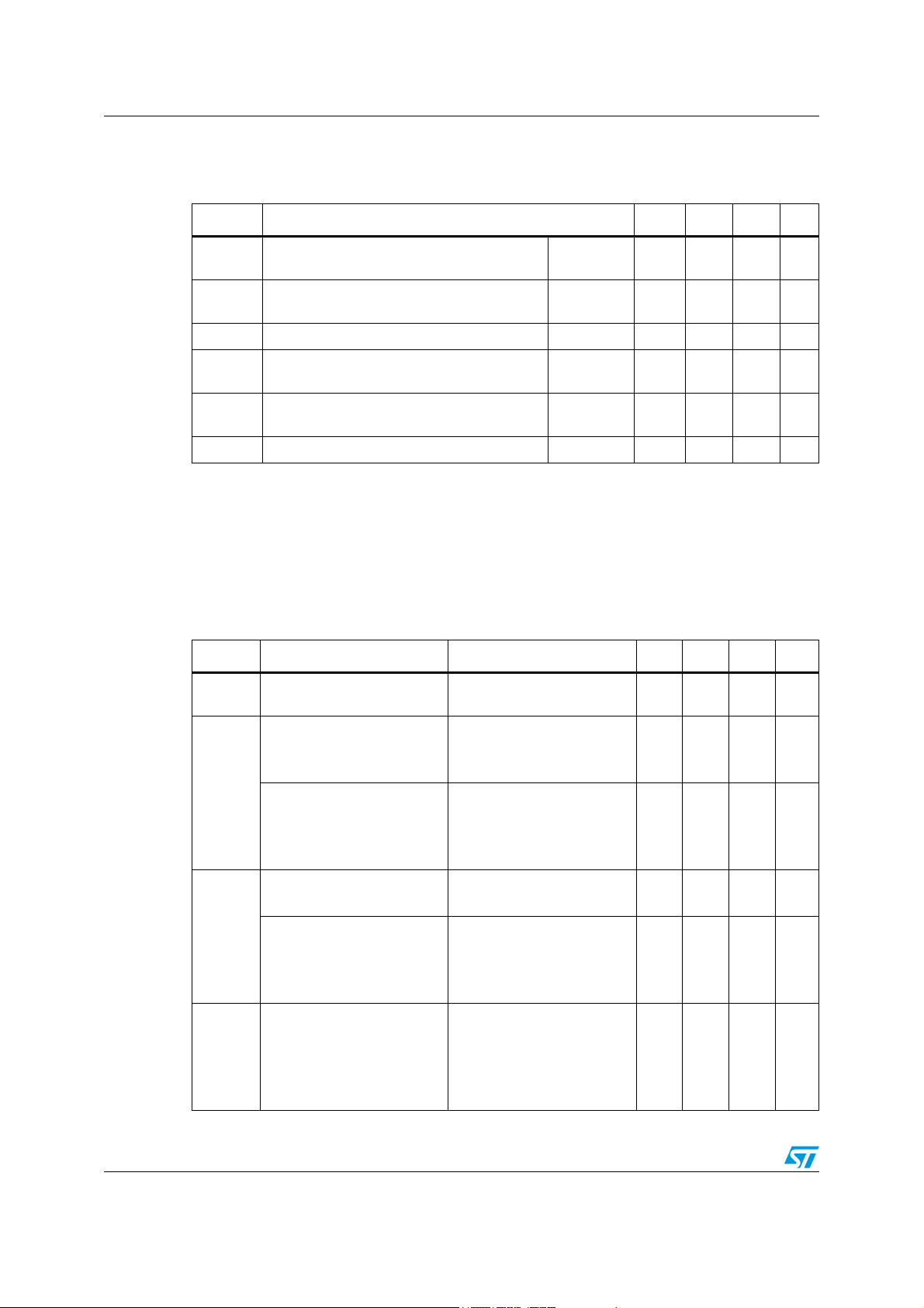
1 Block diagram and pin description
Figure 1. Block diagram
V
BAT
* Note: Value of capacitor has to be choosen carefully to limit the VS
voltage below absolute maximum ratings in case of an unexpected
freewheeling condition of inductive loads (e.g. TSD, POR)
Reverse
Polarity
Protection
100k
VREG
VCC
*
100µF
100nF
EMC
Optimization
100 10
100nF
**
1k
**
1k
**
1k
**
1k
**
1k
+
PWM1
DO
CLK
CSN
DI
VCC
VS
Charge
Pump
SPI
CP
Interface
µC
CM / PWM2
**
1k
Table 2. Pin definitions and functions
MUX
10k
xy-Mirror
OUT1
Motors
OUT2
M
OUT3
M
OUT4
M
Lock
OUT5
Safe Lock
OUT6
OUT7
OUT8
Driver Interface & Diagnostic
GND
** Note: Resistors between µC and L9950 are recommended to limit currents
for negative voltage transients at VBAT (e.g. ISO type 1 pulse)
+ Note: Using a ferrite instead of 10ohm will additionally improve EMC behavior
OUT9
OUT10
OUT11
5
M
Folder
M
Exterior Light
Footstep Light
Safety Light
Turn Indicator
Defroster
Pin Symbol Function
Ground.
1, 18, 19, 36 GND
Reference potential.
Important: for the capability of driving the full current at the outputs all
pins of GND must be externally connected.
Highside driver output 11.
The output is built by a highside switch and is intended for resistive
loads, hence the internal reverse diode from GND to the output is
missing. For ESD reason a diode to GND is present but the energy
2, 35 OUT11
which can be dissipated is limited. The highside driver is a power
DMOS transistor with an internal parasitic reverse diode from the
output to VS (bulk-drain-diode). The output is over-current and open
load protected.
Important: for the capability of driving the full current at the outputs both
pins of OUT11 must be externally connected.
6/39 Doc ID 10311 Rev 10
L9950 - L9950XP Block diagram and pin description
Table 2. Pin definitions and functions (continued)
Pin Symbol Function
Hal bridge output 1,2,3.
3
4
5
OUT1
OUT2
OUT3
6, 7, 14, 15,
23, 24, 25, 28,
VS
29, 32
8DI
9
CM/PWM2
The output is built by a highside and a lowside switch, which are
internally connected. The output stage of both switches is a power
DMOS transistor. Each driver has an internal parasitic reverse diode
(bulk-drain-diode: highside driver from output to VS, lowside driver from
GND to output). This output is over-current and open load protected.
Power supply voltage (external reverse protection required.
For this input a ceramic capacitor as close as possible to GND is
recommended.
Important: for the capability of driving the full current at the outputs all
pins of VS must be externally connected.
Serial data input.
The input requires CMOS logic levels and receives serial data from the
microcontroller. The data is an 24bit control word and the least
significant bit (LSB, bit 0) is transferred first.
Current monitor output/PWM2 input.
Depending on the selected multiplexer bits of Input Data Register this
output sources an image of the instant current through the
corresponding highside driver with a ratio of 1/10.000. This pin is
bidirectional. The microcontroller can overdrive the current monitor
signal to provide a second PWM input for the outputs OUT9 and
OUT10.
Chip select not input/test mode.
This input is low active and requires CMOS logic levels. The serial data
10 CSN
transfer between L9950 and micro controller is enabled by pulling the
input CSN to low level. If an input voltage of more than 7.5V is applied
to CSN pin the L9950 will be switched into a test mode.
Serial data output.
11 DO
The diagnosis data is available via the SPI and this tristate output. The
output will remain in tristate, if the chip is not selected by the input CSN
(CSN = high).
Logic supply voltage.
12 VCC
For this input a ceramic capacitor as close as possible to GND is
recommended.
Serial clock input.
13 CLK
This input controls the internal shift register of the SPI and requires
CMOS logic levels.
16,17, 20,21,
22
OUT4
OUT5
OUT6
Half bridge output 4,5,6: see OUT1 (pin 3).
Important: for the capability of driving the full current at the outputs both
pins of OUT4 (OUT5, respectively) must be externally connected.
Charge pump output.
26 CP
This output is provided to drive the gate of an external n-channel power
MOS used for reverse polarity protection
Doc ID 10311 Rev 10 7/39

Block diagram and pin description L9950 - L9950XP
Table 2. Pin definitions and functions (continued)
Pin Symbol Function
PWM1 input.
27 PWM1
This input signal can be used to control the drivers OUT1-OUT8 and
OUT11 by an external PWM signal.
Highside driver output 7,8,9,10.
30
31
33
34
OUT7,
OUT8,
OUT9,
OUT10
The output is built by a highside switch and is intended for resistive
loads, hence the internal reverse diode from GND to the output is
missing. For ESD reason a diode to GND is present but the energy
which can be dissipated is limited. The highside driver is a power
DMOS transistor with an internal parasitic reverse diode from the
output to VS (bulk-drain-diode). The output is over-current and open
load protected.
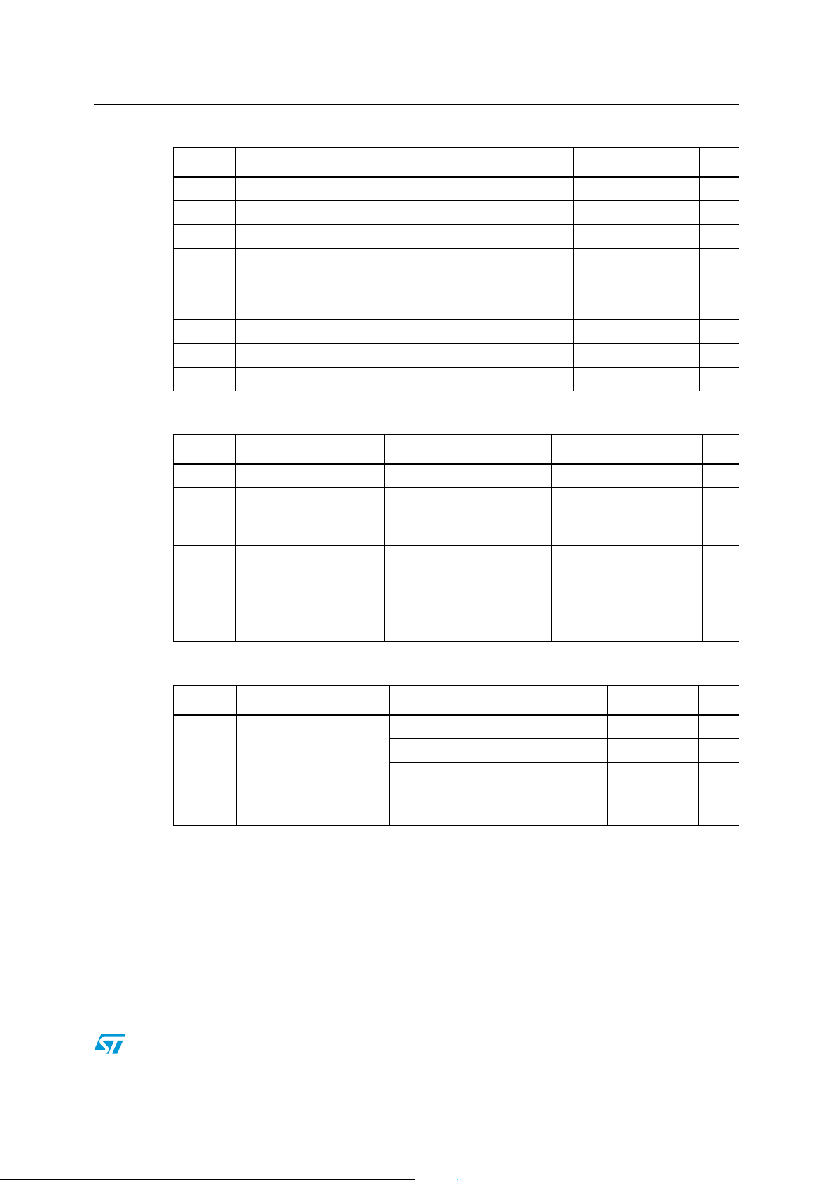
Figure 2. Configuration diagram (top view)
GND 1
OUT11 2
OUT1 3
OUT2 4
OUT3 5
VS 6
VS 7
DI
CM/PWM2 9
CSN 10
DO 11
VCC 12
CLK 13
VS 14
VS 15
OUT4 16
OUT4
GND 18
GND36
Power SO36
8
Chip
17
Leadframe
OUT1135
OUT1034
OUT933
VS32
31 OUT8
30
OUT7
VS
29
VS28
PWM127
CP26
VS25
VS24
VS23
OUT622
OUT521
OUT5
20
GND19
8/39 Doc ID 10311 Rev 10
L9950 - L9950XP Electrical specifications
2 Electrical specifications
2.1 Absolute maximum ratings
Stressing the device above the rating listed in the “Absolute maximum ratings” table may
cause permanent damage to the device. These are stress ratings only and operation of the
device at these or any other conditions above those indicated in the Operating sections of
this specification is not implied. Exposure to Absolute Maximum Rating conditions for
extended periods may affect device reliability. Refer also to the STMicroelectronics SURE
Program and other relevant quality document.
Table 3. Absolute maximum ratings
Symbol Parameter Value Unit
V
S
V
CC
V
, V
DI
DO, VCLK
V
CSN, Vpwm1
V
CM
V
CP
I
OUT1,2,3,6,7,8,9,10
I
OUT4,5,11
,
2.2 ESD protection
Table 4. ESD protection
Output pins: OUT1 - OUT11 ±8
1. HBM according to CDF-AEC-Q100-002.
2. HBM with all unzapped pins grounded.
DC supply voltage -0.3 to 28 V
Single pulse t
< 400 ms 40 V
max
Stabilized supply voltage, logic supply -0.3 to 5.5 V
Digital input/output voltage -0.3 to V
+ 0.3 V
CC
Current monitor output -0.3 to VCC + 0.3 V
Charge pump output -25 to VS + 11 V
Output current ±5 A
Output current ±10 A
Parameter Value Unit
All pins ±4
(1)
(2)
kV
kV
2.3 Thermal data
Table 5. Thermal data
Symbol Parameter Value Unit
T
j
Operating junction temperature -40 to 150 °C
Doc ID 10311 Rev 10 9/39
Electrical specifications L9950 - L9950XP
2.4 Temperature warning and thermal shutdown
Table 6. Temperature warning and thermal shutdown
Symbol Parameter Min. Typ. Max. Unit
T
jTW ON
T
jTW OFF
T
jTW HYS
T
jSD ON
T
jSD OFF
T
jSD HYS
Temperature warning threshold junction
temperature
Temperature warning threshold junction
temperature
Temperature warning hysteresis - 5 - °K
Thermal shutdown threshold junction
temperature
Thermal shutdown threshold junction
temperature
Thermal shutdown hysteresis - 5 - °K
2.5 Electrical characteristics
VS = 8 to 16 V, VCC = 4.5 to 5.3 V, Tj = - 40 to 150 °C, unless otherwise specified.
The voltages are referred to GND and currents are assumed positive, when the current
flows into the pin.
Table 7 . Suppl y
Symbol Parameter Test condition Min. Typ. Max. Unit
V
I
IS + I
Operating supply voltage
S
range
VS DC supply current
I
S
VS quiescent supply current
VCC DC supply current
CC
VCC quiescent supply
current
Sum quiescent supply
CC
current
increasing
decreasing
increasing
decreasing
V
= 16 V, VCC = 5.3 V
S
active mode
OUT1 - OUT11 floating
VS = 16 V, VCC = 0 V
standby mode
OUT1 - OUT11 floating
=-40 °C, 25 °C
T
test
V
= 16 V, VCC = 5.3 V
S
CSN = V
= 16 V, VCC = 5.3 V
V
S
CSN = V
active mode
CC ,
standby mode
CC
OUT1 - OUT11 floating
=-40 °C, 25 °C
T
test
= 16 V, VCC = 5.3 V
V
S
CSN = V
CC
standby mode
OUT1 - OUT11 floating
=-40 °C, 25 °C
T
test
Tj
Tj
Tj
Tj
--150°C
130 - - °C
--170°C
150 - - °C
7-28V
-720mA
- 4 12 µA
-13mA
-2550µA
-3175µA
10/39 Doc ID 10311 Rev 10
L9950 - L9950XP Electrical specifications
0
-
Table 8. Overvoltage and under voltage detection
Symbol Parameter Test condition Min. Typ. Max. Unit
V
SUV ON
V
SUV OFF
V
SUV hyst
V
SOV OFF
V
SOV ON
V
SOV hyst
V
POR OFF
V
POR ON
V
POR hyst
Table 9. Current monitor output
VS UV-threshold voltage VS increasing 5.9 - 7.2 V
VS UV-threshold voltage VS decreasing 5.5 - 6.5 V
VS UV-hysteresis V
SUV ON
- V
SUV OFF
-0.5- V
VS OV-threshold voltage VS increasing 18 - 24.5 V
VS OV-threshold voltage VS decreasing 17.5 - 22 V
VS OV-hysteresis V
SOV OFF
- V
SOV ON
-1-V
Power-on-reset threshold VCC increasing - - 4.4 V
Power-on-reset threshold VCC decreasing 3.1 - - V
Power-on-reset hysteresis V
POR OFF
- V
POR ON
-0.3- V
Symbol Parameter Test condition Min. Typ. Max. Unit
V
I
CM,r
I
CM acc
Functional voltage range VCC = 5 V 0 4 V
CM
Current monitor output
ratio:
I
CM/IOUT1,4,5,6,11
Current monitor accuracy
0V ≤ V
CM
0V ≤ V
CM
= 5 V, I
V
CC
I
Out4,5,11,max
I
Out1,6,max
≤ 4V, VCC=5V - - -
≤ 3.8 V,
=500 mA,
Out,min
= 5.9 A
-
= 2.9 A
1
-----------------
10.00
4% +
1%FS
8% +
2%FS
(FS = full scale= 600 µA)
-
Table 10. Charge pump output
Symbol Parameter Test condition Min. Typ. Max. Unit
V
= 8 V, I
V
I
Charge pump output
CP
voltage
Charge pump output
CP
current
S
= 10 V, I
V
S
V
≥ 12 V, ICP = -100 µA 10 - 13 V
S
V
= VS+10 V, VS =13.5 V 95 150 300 µA
CP
= -60 µA 6 - 13 V
CP
= -80 µA 8 - 13 V
CP
Doc ID 10311 Rev 10 11/39
Electrical specifications L9950 - L9950XP
Table 11. OUT1 - OUT11
Symbol Parameter Test condition Min. Typ. Max. Unit
VS = 13.5 V, Tj = 25 °C,
I
= ± 1.5A
OUT1,6
V
r
ON OUT1,
r
ON OUT6
On-resistance to supply or
GND
= 13.5 V, Tj = 125 °C,
S
I
= ± 1.5 A
OUT1,6
V
= 8.0 V, Tj = 25 °C,
S
I
= ± 1.5 A
OUT1,6
VS = 13.5 V, Tj = 25 °C,
I
= ± 0.8A
OUT2,3
V
r
ON OUT2,
r
ON OUT3
r
ON OUT4,
r
ON OUT5
r
ON OUT7,
r
ON OUT8,
r
ON OUT9 ,
r
ON OUT10
r
ON OUT11
|I
OUT1
|I
OUT6
|I
OUT2
|I
OUT3
|I
OUT4
|I
OUT5
|I
OUT7
|I
OUT8
|I
OUT9
|I
OUT10
On-resistance to supply or
GND
On-resistance to supply or
GND
On-resistance to supply
On-resistance to supply
|,
Output current limitation to
|
supply or GND
Output current limitation to
|,
|
supply or GND
Output current limitation to
|,
|
supply or GND
|,
Output current limitation to
|,
GND
|,
|
= 13.5 V, Tj = 125 °C,
S
I
= ± 0.8 A
OUT2,3
V
= 8.0 V, Tj = 25 °C,
S
I
= ± 0.8 A
OUT2,3
VS = 13.5 V, T
= ± 3.0 A
I
OUT4,5
V
= 13.5 V, Tj = 125 °C,
S
= ± 3.0 A
I
OUT4,5
V
= 8.0 V, Tj = 25 °C,
S
= ± 3.0 A
I
OUT4,5
= 13.5 V, Tj = 25 °C,
V
S
I
OUT7,8,9,10
V
= 13.5 V, Tj = 125 °C,
S
I
OUT7,8,9,10
V
= 8.0 V, Tj = 25 °C,
S
I
OUT7,8,9,10
= 13.5 V, Tj = 25 °C,
V
S
= - 3.0 A
I
OUT11
V
= 13.5 V, Tj = 125 °C,
S
= - 3.0A
I
OUT11
V
= 8.0 V, Tj = 25 °C,
S
= - 3.0 A
I
OUT11
= 25 °C,
j
= -0.8 A
= -0.8 A
= -0.8 A
Sink and source,
VS=13.5V
Sink and source,
= 13.5V
V
S
Sink and source,
= 13.5V
V
S
Source, V
= 13.5V 1.5 - 2.5 A
S
-300400mΩ
-450600mΩ
-300400mΩ
- 800 1100 mΩ
- 1250 1700 mΩ
- 800 1100 mΩ
-150200mΩ
-225300mΩ
-150200mΩ
- 800 1100 mΩ
- 1250 1700 mΩ
- 800 1100 mΩ
-100150mΩ
-150200mΩ
-100150mΩ
3-5A
1.5 - 2.5 A
6-10A
12/39 Doc ID 10311 Rev 10
 Loading...