


■
ONE FULL BRIDGE FOR 6A LOAD (ron= 150mΩ)
■ THREE HALF BRIDGES FOR 1.6 A LOAD
(r
= 800mΩ)
on
■ ONE HIGHSIDE DRIVER FOR 6A LOAD
(r
= 100mΩ)
on
■ VERY LOW CURRENT CONSUMPTION IN
STANDBY MODE (I
■ SERIAL PERIPHERAL INTERFACE (SPI) TO
< 6µA, typ. Tj ≤ 85°C)
S
MICROCONTROLLER
■
ALL OUTPUTS SHORT CIRCUIT PROTECTED
■ CURRENT MONITOR OUTPUT FOR FULL
BRIDGE AND HIGHSIDE DRIVER
■ ALL OUTPUTS OVER TEMPERATURE
PROTECTED
■
OPEN LOAD DIAGNOSTIC FOR ALL OUTPUTS
■
OVERLOAD DIAGNOSTIC FOR ALL OUTPUTS
L9949
DOOR ACTUATOR DRIVER
MULTIPOWER BCD60III TECHNOLOGY
PowerSO20
ORDERING NUMBER: L9949
FULL BRIDGE FOR DOOR LATCH OR
MIRROR RETRACT, HALF BRIDGES FOR
MIRROR AXIS CONTROL AND HIGH-SIDE
DRIVER FOR MIRROR DEFROSTER
APPLICATIONS
■ FOR AUTOMOTIVE APPLICATI ONS, E.G.
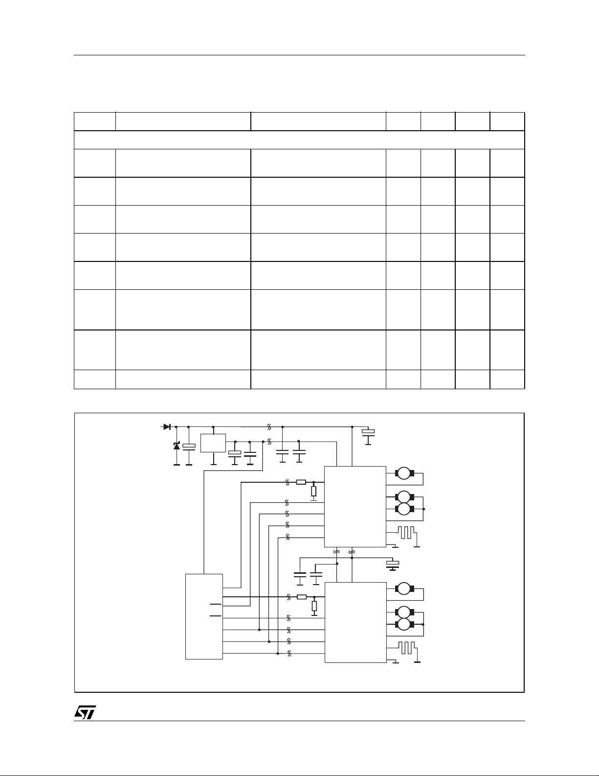
BLOCK DIAGRAM
V
CC
CM
MUX
DI
DO
µC
CLK
CSN
SPI
Driver Interface & Diagnostic
DESCRIPTION
The L9949 is a microprocessor control led power interface for automotive applications. It is realized in
multipower BCD60III technology. Up to three D C mo-
V (battery)
S
OUT1
Full bridge
OUT2
OUT3
Half bridge
OUT4
Half bridge
OUT5
OUT6
Highside driver
M
M
M
e.g. for mirror retract
or door latch
e.g. for mirror
axis control
e.g. for mirror
defroster
September 2002
Ground
1/20

L9949
DESCRIPTION
(continued)
tors and one grounded resistive load can be driven with its three half bridges, one full bridge and one highside
driver power outputs. The integrated standard serial peripheral interface (SPI) controls all operation modes (forward, reverse, brake and high impedance). All diagnostic informations are available via the SPI.
Dual Power Supply: VS and V
CC
The power supply voltage VS supplies the ful l bridge, the half bridges and the highside driver. An internal
charge-pump are used to drive the highside switches. The logic supply voltage V
(stabilized 5V) is used for
CC
the logic part and the SPI of the device. Due to the independent logic supply voltage the control and status information will not be lost, if there are temporary spikes or glitches on the power supply voltage. In case of poweron (V
power-on-reset (POR). If the voltage V
increases from undervoltage t o V
CC
VCC OFF
decreases under the minimum threshold (V
CC
= 4.2V) the ci rcuit i s ini tialized by an internall y generated
VCC ON
= 3.4V), the out-
puts are switched to tristate (high impedance) and the status registers are cleared.
Standby-Mode
The standby mode of the L9949 is activated by setting the bits 12 and 13 of the Input Data Register to zero. All
latched data will be cleared and the inputs and out puts are switc hed to high impedance. In t he st andby mode
the current at V
(VCC) is less than typ. 6µA (40µA) for CSN = high (DO in tristate). By switching the VCC voltage
S
a very low quiescent current can be achieved. If one of the bits 12 and 13 are set to high, the device will be
switched to active mode.
Inductive Loads
Each half bridge is built by internally connected highside and a lowside power DMOS transistor. Due to the builtin reverse diodes of the output transistors inductive loads can be driven at the outputs OUT1 to OUT5 without
external free-wheeling diodes. The highside driver OUT6 is intended to drive resistive loads only hence only a
limited energie (E<1mJ ) can be dissipated by the i nt ernal ESD-diode in f reewheeli ng conditi on. For i nduct ive
loads (L>100
µ
H) an external free-wheeling diode connected to GND and OUT6 is needed.
Diagnostic Functions
All diagnostic functions (over /open load, power supply over-/undervoltage, temperature warning and thermal
shutdown) are internally filtered and the condition has to be valid for at least 10µs (0.5ms, respectively) before
the corresponding status bit in the status registers will be set. The filters are used to improve the noise immunity
of the device. The open load and temperature warning function are intended for informati on purpose and will
not change the state of the output drivers. In contrast, the overload and thermal shutdown condition will disable
the corresponding driver (overload) or all dr ivers ( t hermal shut down), respectiv ely. The micr ocontroller has to
clear the status bits to reactivate the corresponding drivers. This is to avoid an uncontrolled switching behaviour
of the device which may result in a heavy noise on the GND and V
to GND o r V
).
S
lines in case of an fault condition (e.g. short
S
Overvoltage and Undervoltage Detection
If the power supply voltage VS rises above the overvoltage threshold V
SOV OFF
(max. 22V), the outputs OUT1
to OUT6 are switched to high impedance state to protect the load. If the supply voltage recovers to normal operating voltage, the device will return to the programmed state (lockout bit 14 = 0). When the voltage V
below the undervoltage threshold V
SUV OFF
(min. 6V), the output stages are switc hed to high impedance to
drops
S
avoid the operation of the power devices without sufficient gate driving voltage (increased power dissipation). If
the supply voltage V
and the internal charge-pump recovers to normal operating voltage the syste m returns to
S
the programmed state (lockout bit 14 = 0). If the lockout bit 14 is set, the automatic turn-on of the drivers is deactivated. The microcontroller needs to clear the status bits to reactivate the drivers.
2/20

L9949
Temperature Warning and Thermal Shutdown
When the junction temperature rises above T
If the junction temperature increases above the second threshold T
the power DMOS transistors of the out put stages are switched off to protect the devic e. I n order t o reac tivate
the output stages the junction temperature must decrease below T
has to be cleared by the microcontroller.
Open Load Detection
The open load detection monitors the voltage drop of current sense resistors in each highside and lowside driver
of the output stage. The output s i gnal of an open l oad comparator has to be v al id for at l east 0.5 ms (t
set the open load bit (bit 1-11) in the status register 1.
Over Load Detection
In the case of an overcurrent condition an overcurrent fl ag (bit 1-11) is set in the stat us regist er 0 i n the same
way as open load detection. If the overcurrent signal is valid for at least t
and the corresponding driver is switched off to reduce the power dissipation and to protect the integrated circuit.
The microcontroller has to clear the status bits to reactivate the corresponding driver.
Current monitor
The current monitor output sources a current image at the current monitor output which has a fi xed ratio (1/
10000) of the instantaneous current of the selected highside driver. The bits 12 and 13 of the Input Data register
controls which of the outputs OUT1, OUT2 and OUT6 will be multiplexed to the current monitor output. The current monitor output allows a more precise analyse of the actual s tate of the load rather than the detection of an
open- or overload condition. For example this can be used to detect the motor state (free-running, loaded or
blocked) or the temperature of the heating element.
a temperature warning flag is set and is available via the SPI.
j TW
, the thermal shutdown bit will be set and
j SD
j SD
- T
j SD HYS
ISC
and the thermal shutdown bit
= 10µs, the overcurrent flag is set
dOL
) to
Figure 1. Pin Connection (Top view)
GND GND
OUT3 OUT6
OUT4
OUT5
VS
CLK
DI
VS
OUT1
GND
1
2
3
4
5
6
7
8
9
D99AT455Amod
20
19
18
17
16
15
14
13
12
11
VS
DO
CM
VCC
CSN
VS
OUT2
GND10
3/20

L9949
PIN FUNCTION
N° Pin Description
1, 10,
11, 20
5, 8, 13, 18V
15 V
14 CSN Chip Select Not input:
6CLKSerial clock input:
7 Data In Serial data input:
17 Data Out Serial data output:
16 CM Current monitor output:
GND Ground:
Reference potential
Important:
externally connected !
Power supply voltage (battery):
S
For this input a ceramic capacitor as close as possible to GND is recommended.
Important:
externally connected !
Logic supply voltage:
CC
For this input a ceramic capacitors as close as possible to GND are recommended.
This input is low active and requires CMOS logic levels. The serial data transfer between L9949
and micro controller is enabled by pulling the input CSN to low level. If an input voltage of more
than 9.6V above VCC is applied to CSN pin the L9949 will be switched into a test mode.
This input controls the internal shift register of the SPI and requires CMOS logic levels.
The input requires CMOS logic levels and receives serial data from the microcontroller. The data
is an 16bit control word and the least significant bit (LSB, bit 0) is transferred first.
The diagnosis data is available via the SPI and this tristate-output. The output will remain in
tristate, if the chip is not selected by the input CSN (CSN = high)
Depending on the multiplexer bits 12 and 13 of the Input Data register this output sources an
image of the instant current through the corresponding highside driver with a ratio of 1/10000
For the capability of driving the full current at the outputs all pins of GND must be
For the capability of driving the full current at the outputs all pins of VS must be
9OUT1Halfbridge-output 1:
The output is built by a highside and a lowside switch, which are internally connected. The
output stage of both switches is a power DMOS transistor. Each driver has an internal parasitic
reverse diode (bulk-drain-diode, highside driver from OUT1 to V
OUT1). This output is overcurrent and open load protected.
12 OUT2
2OUT3Halfbridge-output 3:
3OUT4
4OUT5
19 OUT6 Highside-driver-output 6:
Halfbridge-output 2:
The output is built by a highside and a lowside switch, which are internally connected. The
output stage of both switches is a power DMOS transistor. Each driver has an internal parasitic
reverse diode (bulk-drain-diode, highside driver from OUT3 to VS, lowside driver from GND to
OUT3). This output is overcurrent and open load protected.
Halfbridge-output 4:
Halfbridge-output 5:
The output is built by a highside switch and can be used only for a resistive load, because the
internal reverse diode from GND to OUT6 is missing. This highside switch is a power DMOS
transistor with an internal parasitic reverse diode from OUT6 to V
is overcurrent and open load protected.
→ see OUT1 (pin 9)
→ see OUT3 (pin 2)
→ see OUT3 (pin 2)
, lowside driver from GND to
S
(bulk-drain-diode). The output
S
4/20

ABSOLUTE MAXIMUM RATINGS
Symbol Parameter Value Unit
L9949
V
V
CC
VDI VDO
V
CLK
V
CSN
V
CM
I
OUT1,OUT2,
OUT6
I
OUT3,OUT5
Note: All m axim um ra tin gs are a bsol ute r atings . Leav ing the l imi tatio n of any one of thes e val ues m ay c ause an irre vers ibl e dam age of the
integrated circuit!
DC supply voltage -0.3...28 V
S
single pulse t
< 400 ms 40 V
max
stabilized supply voltage, logic supply -0.3 to 6 V
digital input / output voltage -0.3 to VCC + 0.3 V
,
current monitor output -0.3 to VCC + 0.3 V
output current ±10 A
output current ±5 A
ESD PROTECTION
Parameter Value
All pins
output pins: OUT1 – OUT6
(1) HBM according to MIL 883C, Methode 3015.7 or EIA/JESD22-A114-A
(2) HBM with all unzapped pins grounded
±2
±4
(1)
(2)
kV
kV
THERMAL DATA
Symbol Parameter Value Unit
Operating junction temperature:
T
Temperature warning and thermal shutdown:
Symbol Parameter Min. Typ. Max. Unit
T
jTW ON
T
jTW OFF
T
jTW HYS
T
jSD ON
T
jSD OFF
T
jSD HYS
Operating Junction Temperature -40 to 150 °C
j
Temperature Warning Threshold
Tj increasing 150 °C
Junction Temperature
Temperature Warning Threshold
Tj decreasing 120 °C
Junction Temperature
Temperature Warning Hysteresis 10 K
Thermal Shutdown Threshold
Tj increasing 180 °C
Junction Temperature
Thermal Shutdown Threshold
Tj decreasing 150 °C
Junction Temperature
Thermal Shutdown Hysteresis 10 K
5/20

L9949
Figure 2. Thermal Data of Package
Z (˚C/W)
th
PowerSO20 Z
th(j-a)
1x1 sq. mm
2x2 sq. mm
3x3 sq. mm
silicon
diss. area dimensions
10
diss. area
1
die size 6x6 sq. mm
0.1
4x4 sq. mm
5x5 sq. mm
mounted on standard board
T = 20˚C
amb
still air
dissipated power 1 W - single pulse
diss. area located in a corner
0.001 0.01 0.1
1
10 100 1000
Time (s)
ELECTRICAL CHARACTERISTCS
VS=8to16V, VCC= 4.5 to 5.5 V, Tj= -40 to 150 °C, unless otherwise specified. The voltages are refered to
GND and currents are assumed positive, when the current flows into the pin
Symbol Parameter Test Condition Min. Typ. Max. Unit
.
Supply
V
I
I
S+ICC
Operating Supply Voltage
S
Range
I
DC Supply Current active mode,
S
Quiescent Supply Current standby mode,
DC Supply Current active mode, CSN = VCC,
CC
Quiescent Supply Current
Sum Supply Quiescent Current standby mode, CSN = VCC,
=16V, VCC= 5.3 V,
V
S
OUT1 - OUT6 floating
V
=16V, VCC=0V,
S
T
j
OUT1 - OUT6 floating
V
S
standby mode, CSN = VCC,
VS=16V
T
j
OUT1 - OUT6 floating
VS=16V, VCC= 5.3 V, Tj<85°C
OUT1 - OUT6 floating
(1)
<85°C
=16V; VCC= 5.3 V
, VCC= 5.3V,
(1)
<85°C
728V
720mA
612µA
12mA
40 75 µA
50 90 µA
6/20

L9949
ELECTRICAL CHARACTERISTCS
V
=8to16V, VCC= 4.5 to 5.5 V, Tj= -40 to 150 °C, unless otherwise specified. The voltages are refered to
S
GND and currents are assumed positive, when the current flows into the pin
(continued)
.
Symbol Parameter Test Condition Min. Typ. Max. Unit
(1) Param eter is measured at - 40°C and 25°C. Value fo r 85°C is guaranteed by des i gn
Over- and undervoltage detection
V
SUV ONVS
V
SUV OFFVS
V
SUV hystVS
V
SOV OFFVS
V
SOV ONVS
V
SOV
hyst
V
VCC OFF
V
VCC ON
V
VCC
hyst
UV-Threshold Voltage VS increasing 7.6 V
UV-Threshold Voltage VS decreasing 6 V
UV-hysteresis V
SUV ON
– V
SUV OFF
0.6 V
OV-threshold voltage VS increasing 22 V
OV-threshold voltage VS decreasing 18 V
VS OV-hysteresis V
SOV OFF
– V
SOV ON
1V
Power-on-reset Threshold VCC increasing 4.2 V
Power-on-reset Threshold VCC decreasing 3.4 4 V
Power-on-reset Hysteresis V
VCC OFF
– V
VCC ON
0.3 V
Current Monitor Output
V
I
CM,r
I
CM acc
Functional Voltage Range VCC=5V 0 4 V
CM
Current Monitor Output Ratio:
I
CM/IOUT1,2,6
Current Monitor Accuracy 0V ≤ VCM ≤ 4V,
Outputs: OUT1 - OUT6
R
ON OUT1
R
ON OUT2
On-resistance to Supply or GND VS= 13.5 V, Tj= 25 °C,
On-resistance to Supply or GND VS= 1 3.5 V, Tj= 25 ° C,
0V≤VCM≤ 4V -
=50µA, 600 µA
I
CM
(FS=full scale=600µA)
1
----------------
10000
4%
+
1%FS
8%
+
2%FS
150 mΩ
I
= ±3.0 A
OUT1
VS= 1 3.5 V, Tj= 125 °C,
I
= ± 3.0 A
OUT1
VS= 8.0 V, Tj=25°C,
I
= ± 3.0 A
OUT1
225 mΩ
180 mΩ
150 mΩ
I
= ± 3.0 A
OUT2
= 1 3.5 V, Tj= 125 °C,
V
S
I
= ± 3.0 A
OUT2
VS= 8.0 V, Tj=25°C,
I
= ± 3.0 A
OUT2
225 mΩ
180 mΩ
7/20
L9949
ELECTRICAL CHARACTERISTCS
V
=8to16V, VCC= 4.5 to 5.5 V, Tj= -40 to 150 °C, unless otherwise specified. The voltages are refered to
S
GND and currents are assumed positive, when the current flows into the pin
(continued)
.
Symbol Parameter Test Condition Min. Typ. Max. Unit
R
ON OUT3
R
ON OUT4
R
ON OUT5
On-resistance to Supply or GND VS= 1 3.5 V, Tj= 25 ° C,
I
= ± 0.8 A
OUT3
VS= 1 3.5 V, Tj= 125 °C,
I
= ± 0.8 A
OUT3
VS= 8.0 V, Tj=25°C,
I
= ± 0.8 A
OUT3
On-resistance to Supply or GND VS= 1 3.5 V, Tj= 25 ° C,
I
= ± 0.8 A
OUT4
VS= 1 3.5 V, Tj= 125 °C,
I
= ± 0.8 A
OUT4
VS= 8.0 V, Tj=25°C,
I
= ± 0.8 A
OUT4
On-resistance to Supply or GND VS= 1 3.5 V, Tj= 25 ° C,
I
= ± 0.8 A
OUT5
VS= 1 3.5 V, Tj= 125 °C,
I
= ± 0.8 A
OUT5
800 mΩ
1250 mΩ
980 mΩ
800 mΩ
1250 mΩ
980 mΩ
800 mΩ
1250 mΩ
R
ON OUT6
|I
OUT1
On-resistance to Supply VS= 1 3.5 V, Tj= 25 ° C,
| Output Current Limitation to
VS= 8.0 V, Tj=25°C,
I
= ± 0.8 A
OUT5
I
= - 2.5 A
OUT6
= 1 3.5 V, Tj= 125 °C,
V
S
I
= - 2.5 A
OUT6
= 8.0 V, Tj=25°C,
V
S
I
= - 2.5 A
OUT6
sink and source, current ramp 6 10 A
980 mΩ
100 mΩ
150 mΩ
120 mΩ
Supply or GND
|I
| Output Current Limitation to
OUT2
sink and source, current ramp 6 10 A
Supply or GND
|I
| Output Current Limitation to
OUT3
sink and source, current ramp 1.6 2.5 A
Supply or GND
|I
| Output Current Limitation to
OUT4
sink and source, current ramp 1.6 2.5 A
Supply or GND
|I
| output current limitation to Supply
OUT5
sink and source, current ramp 1.6 2.5 A
or GND
| Output Current Limitation to GND source, current ramp 6.3 11 A
|I
OUT6
|I
For details of the on-resistance (Ron over temperature) see the figur es „Typical ron characteristics“ for the differential output stages
(FIGURE 3, FIGURE4 , FIGURE 5)
OUT6/res
|
Output Current Limitation to GND
switching into resistive load
source, switching into resistive
load, go-nogo test
5.1 11 A
8/20

Figure 3. TYP ICAL RON CHARACTERISTICS OUT1,2
V
160
140
120
100
L9949
80
60
Ron [mOhm]
40
20
0
-40 -20 0 20 40 60 80 100 120
TEMP [C]
Figure 4. TYP ICAL RON CHARACTERISTICS OUT3,4,5
1100
1000
900
800
700
HS 13.5V
HS 8V
LS 13.5
LS 8V
600
500
400
Ron [mOhm]
300
200
100
0
-40 -20 0 20 40 60 80 100 120
HS 13.5V
HS 8
LS 13.5
LS 8V
TEMP [C]
9/20

L9949
0
Figure 5. TYP ICAL RON CHARACTERISTICS OUT6
110
100
90
80
70
60
50
Ron [m Ohm]
40
30
20
10
0
-40 -20 0 2
40 60 80 100 120
TEMP [C]
HS 13.5V
HS 8V
ELECTRICAL CHARACTERISTCS
VS=8to16V, VCC= 4.5 to 5.5 V, Tj= -40 to 150 °C, unless otherwise specified. The voltages are refered to
GND and currents are assumed positive, when the current flows into the pin
Symbol Parameter Test Condition Min. Typ. Max. Unit
OUTPUTS: OUT1 - OUT6
t
d ON H
Output Delay Time,
Highside Driver On
t
d OFF H
Output Delay Time,
Highside Driver Off
t
d ON L
Output Delay Time,
Lowside Driver On
t
d OFF L
Output Delay Time,
Lowside Driver Off
t
D HL
t
D LH
I
QLH
Dead Time, Source to Sink t
Dead Time, Sink to Source t
Leakage Current Highside
Drivers of OUT1-6
VS= 13,5 V
corresponding low side driver is
not active
VS= 13,5 V 80 150 300 µs
VS= 13,5 V
corresponding highside driver is
not active
VS= 13.5 V 80 150 300 µs
(HS was on) - t
d ON L
d ON H
V
OUT1-6
V
OUT1-6
(LS was on) - t
= 0 V, standby mode 0 2 5 µA
= 0 V, active mode -40 -15 0 µA
d OFF H
d OFF L
.
20 40 80 µs
20 40 80 µs
5200µs
5200µs
I
QLL
Leakage Current Lowside Drivers
V
OUT1-5=VS
, standby mode 0 7 20 µA
of OUT1-5
V
OUT1-5=VS
, active mode -40 -15 0 µA
10/20
L9949
ELECTRICAL CHARACTERISTCS
V
=8to16V, VCC= 4.5 to 5.5 V, Tj= -40 to 150 °C, unless otherwise specified. The voltages are refered to
S
GND and currents are assumed positive, when the current flows into the pin
(continued)
.
Symbol Parameter Test Condition Min. Typ. Max. Unit
OUTPUTS: OUT1 - OUT6
I
OLD12
Open Load Detection Current of
80 160 320 mA
OUT1 and OUT2
I
OLD345
Open load detection current of
20 40 60 mA
OUT3, OUT4 and OUT5
I
OLD6
open load detection current of
60 160 320 mA
OUT6
t
dOL
minimum duration of open load
500 3000 µs
condition to set the status bit
t
minimum duration of overcurrent
ISC
10 100 µs
condition to switch off the driver
dV
/d
t
dV
OUT12
OUT345
slew rate of OUT1 and OUT2 VS=13.5V,
for highside driver: I
for lowside driver: I
/d
t
slew rate of OUT3, OUT4 and
OUT5
VS=13.5V,
for highside driver: I
for lowside driver: I
load
load
load
load
= -3A,
= 3A
= -0.8A,
= 0.8A
0.1 0.2 0.4 V/µs
0.09 0.2 0.4 V/µs
dV
/dt
OUT6
slew rate of OUT6 VS=13.5V, I
Figure 6. Application Circuit Diagram
VBAT
5V
STXXX
VCC
CM0
CM1
SS0
SS1
µC
SCK
MOSI
MISO
*in case of an unexpected freewheeling condition (e.g. POR, TSD or OV event) capacitor value
must be high enough to limit maximum Vs voltage of L9949 appl_n_wmf below absolute
maximum ratings.
= -2.5A 0.1 0.2 0.4 V/µs
load
*see comment
below
VCC VS
CM
L9949
CSN
CLK
DI
DO
VCC VS
CM
L9949
CSN
CLK
DI
DO
OUT1
OUT2
OUT3
OUT4
OUT5
OUT6
GND
OUT1
OUT2
OUT3
OUT4
OUT5
OUT6
GND
M
M
M
*see comment
below
M
M
M
11/20

L9949
CLK (pi
)CSN (pi
)
Figure 7. Funct i on a l Bl ock D i agram
OUT1
(pin9)
OUT2
(pin12)
VS (pin8)
VS (pin8)
VS (pin13)
VS (pin13)
HS
A-driver
LS
A-driver
HS
B-driver
LS
B-driver
HS
A-driver
LS
A-driver
HS
B-driver
LS
B-driver
Chargepump
Voltage and
Current
Reference
GND
(pins 1,10,1 1,20 )
Driver Interface
Power-On-Reset
Temperature
Protection
Current
Monitor
VCC
(pin 15)
n 6
SPI
Diagnostic
(pin 16)
CM
DI (pin 7)DO (pin 17)
VCC
n 14
VS
(pins 5,8,13,18)
HS
LS
HS
LS
HS
LS
HS
A-driver
HS
B-driver
VS (pin5)
VS (pin5)
VS (pin5)
VS (pin18)
ESD
VS (pin18)
ESD
OUT5
(pin4)
OUT4
(pin3)
OUT3
(pin2)
OUT6
(pin19)
FUNCTIONAL DESCRIPTION OF THE SPI
Serial Peripheral Interface (SPI)
This device uses a standard SPI to communicate with a microcontroller. The SPI can be driven by a microcontroller
with its SPI peripheral running in either of the two following modes: CPOL = CPHA = 0 or CPOL = CPHA = 1.
For these two modes, input data i s sampled by t he l ow to hi gh t ransi t i on of t he c lock CLK, and out put dat a is
changed from the high to low transition of CLK.
The difference of these two modes is the standby polarity of the CLK. For CPOL = 0 the CLK remains low and
for CPOL = 1 the CLK remains high.
This device is not limited to microcontrollers with a build-in SPI. Only three CMOS-compatible output pins and
one input pin will be needed to communicate with the device. A fault condition can be detected by setting CSN
to low. If CSN = 0, the DO-pin will reflect the status bit 0 (fault condition) of the device which is a logical-or of all
bits in the status regi st ers 0 and 1. The microcontroller can pol l t he st atus of t he device wi thout the need of a
full SPI-communication c ycle.
Note:
In contrast to the SPI-standard the least significant bit (LSB) will be tran sfered first ( s ee. FIGURE 8).
Chip Select not (CSN)
The input pin is used to select the serial interface of this device. When CSN is high, the output pin (DO) will be
in high impedance state. A low signal will activate the output driver and a serial communication can be started.
Serial Data In (DI)
The input pin is used to transfer data serial into the device. The data applied to the DI will be sampled at the
12/20

L9949
rising edge of the CLK signal and shifted into an internal 16 bit shift register. At the rising edge of the CSN signal
the c ontents of the shift re gister will be t ra nsfer ed to Da t a I nput R egister (see FIGURE 8).
The SPI uses an internal 16 bit counter which will be reset at the rising edge of the CSN signal. Only the first 16
bits o f t he data input D I will be releva nt. If mo re than 16 bits are transfered the trailing bits will be ignored.
Serial Data Out (DO)
The output driver is activated by a logical low level at the CSN input and will go from high impedance to a low
or high level depending on the status bit 0 (fault condition). The first rising edge of the CLK input after a high to
low transition of the CSN pin will transfer the content of the selected status register into the data out shift register.
Each subsequent falling edge of the CLK will shift the next bit out.
Serial Clock (CLK)
The CLK input is used to synchronize the input and output serial bit streams. The data input (DI) is sampled at
the rising edge of the CLK and the data output (DO) will change with the falling edge of the CLK signal (see
FIGURE 8).
Input Data Register
After the rising edge of CSN the contents of the input shift register will be written to the input data register. Depending on bit 0 the contents of the selected status register will be transfered to DO during the current communication cycle. Bit 1-11 controls the behaviour of the corresponding driver. If bit 12 and bit 13 are zero, the device
will go into the st andby-mode. I f at l east one of bot h bits are one these bits wil l be used t o cont rol t he current
monitor multiplexer. Bit 14 selects the V
the power supply V
will di sab le a ll driv er stages un til the status bit will be cleared by the microcontroller. Bit 15
S
is used to reset all status bits in both status registers. The bits in the status registers will be cleared after the
current communication cycle (rising edge of CSN).
lockout mode. If this bit i s set, an over- or undervoltage condition at
S
Status Register
This devices uses two status registers to store and to monitor the state of the device. Bit 0 is used as a fault bit
and is a logical-NOR combination of all other bits in both status registers. The state of this bit can be polled by
the microcontroller without the need of a full SPI-communication cycle (see FIGU RE 13). If one of the overcurrent bits is set, the corresponding driver will be disabled. The microcontroller has to clear the overcurrent bit to
enable the driver. If the thermal s hutdown bit is set, al l driv ers will go into a hi gh impedance state. Again the
microcontroller has to clear the bit to enable the drivers. The behaviour of the device in case of an over- or undervoltage condition will depend on the V
device will reactivate the drivers if the power supply V
lockout bit (bit 14) in the input data register. If bit 14 is cleared, the
S
returns to normal operating range. In this case no inter-
S
action from the microcontroller is needed.
Test Mode
Due to the current limitations of a single bond wire the out put stages OUT1, 2 and 6 need two bond wires in
parallel. For the full output current driving capability it is necessary to check that both bond wires are connected
correctly to the lead frame. Therefore the drivers and DMOS-transistors of the outputs OUT1, 2 and 6 are splitted into two independet stages, one for each bond wire (see FIGURE 6.4). In normal operating mode the splitted
outputs are connected in parallel. In the test mode bit 5 and 6 of the input data register select the A-driver, bit 7
and 8 the B-driver. If all four bits (5 - 8) are switched to high level, no driver will be activated. For all combinations
beside both high of bi t 5 and 6 or bit 7 and 8 t he output stages OUT3 and OUT4 are cont rol led like i n normal
operating mode. In any case the output stages are protected against shoot through current. Furthermore the
inputs CLK and DI are connected by an OR to the output DO for testing the threshold voltages and the hysteresis. The input CLK can be tested by clamping the input DI to low level and vice versa.
13/20
L9949
SPI Interface – Input Data and Status Register
Input Data Register Status Register
BIT Function BIT Function
Register 0 Register 1
15 High level reset all bits in selected status
register
14 V
13
under- / overvoltage lockout bit 14 VS overvoltage not used
S
Control bits for standby mode and
Current monitor multiplexer
12
bit13 bit12 function 12 Temperature
0 0 standby mode 11 OUT6 – HS driver
01 OUT1
1 0 OUT2 10 OUT5 – HS driver
11 OUT6
11
10
9
OUT6 – HS drive r on/off
OUT5 – HS drive r on/off
OUT5 – LS driver on/off
8 OUT4 – HS driver
(1)
on/off 5
7 OUT4 – LS driver
(1)
on/off 5
6 OUT3 – HS driver
(1)
on/off 5
5 OUT3 – LS driver
(1)
on/off 5
4
3
2
1
OUT2 – HS drive r on/off 5
OUT2 – LS driver on/off
OUT1 – HS drive r on/off
OUT1 – LS driver on/off
(1)
(1)
(1)
test mode 6 OUT3 – HS driver
bit 8 bit 7
1 1 5 OUT3 – LS driver
B-driver is active
test mode 4 OUT2 – HS driver
bit 6 bit 5
1 1 3 OUT2 – LS driver
A-driver is active
1
1
1
1
0 Status register select bit
L: status register 0; H: status register 1
15 always H always H
13 V
undervoltage chargepump off
S
shutdown
overcurrent
overcurrent
9 OUT5 – LS driver
overcurrent
8 OUT4 – HS driver
overcurrent
7 OUT4 – LS driver
overcurrent
overcurrent
overcurrent
overcurrent
overcurrent
2 OUT1 – HS driver
overcurrent
1 OUT1 – LS driver
overcurrent
0
no fault condition
H = on; L = off; HS = highside; LS = lowside
– set to L
Temperature
warning
OUT6 – HS driver
open load
OUT5 – HS driver
open load
OUT5 – LS driver
open load
OUT4 – HS driver
open load
OUT4 – LS driver
open load
OUT3 – HS driver
open load
OUT3 – LS driver
open load
OUT2 – HS driver
open load
OUT2 – LS driver
open load
OUT1 – HS driver
open load
OUT1 – LS driver
open load
(2)
(1) If the bits of HS- and LS-driver of the same output stage are high, the internal logic prevents that both drivers of this output stage can
be switched on simult aneously in order to avoid a hi gh internal current from V
(2) A logical NOR- combination of all bits 1 to 14 in both sta tus regist ers. Thi s bit can be polle d by the m i cro-controller wi thout the need
of the full SPI communication (see Figure 13). A broken VCC-connection of the L9949 can be detected by the microcontroller, because
all 15 bits l ow or high is not a valid frame.
to GND.
S
14/20

L9949
SPI INTERFACE ELECTRICAL CHARACTERISTCS
VS=8to16V, VCC= 4.5 to 5.5 V, Tj= -40 to 150 °C, unless otherwise specified. The voltages are refered to
GND and currents are assumed positive, when the current flows into the pin
Symbol Parameter Test Condition Min. Typ. Max. Unit
Delay time from standby to active mode
.
t
set
Delay Time
Inputs: CSN, CLK and DI
V
V
V
INHyst
I
CSNin
I
CLK in
I
DI in
C
DI timing (see Fig. 9 )
t
CLK
t
CLKH
t
CLKL
t
set CSN
Input Low Level VCC=5V 1.5 V
INL
Input High Level VCC=5V 3.5 V
INH
Input Hystersis VCC=5V 0.5 V
Pull Up Current at input CSN V
Pull Down Current at input CLK V
Pull Down Current at input DI VDI=1.5V 10 25 50 µA
(1)
Input Capacitance at input CSN
in
or CL K
(2)
Clock Period VCC= 5 V 1000 ns
Clock High Time VCC= 5 V 400 ns
Clock Low Time VCC= 5 V 400 ns
CSN setup time, CSN low before
rising edge of CLK
Switching from standby to active
200 µs
mode. Time until output drivers are
enabled after CSN going to high.
= 3.5 V -50 -25 -10 µA
CSN
=1.5V 10 25 50 µA
CLK
0V<VCC< 5.5 V 10 15 pF
VCC= 5 V 400 ns
t
set CLK
t
set DI
t
hold DI
t
t
DO
V
V
r-in
f-in
DOL
DOH
CLK setup time, CLK high before
VCC= 5 V 400 ns
rising edge of CSN
DI setup time VCC= 5 V 200 ns
DI hold time VCC= 5 V 200 ns
Rise Time of Input Signal
VCC=5V 100 ns
DI, CLK, CSN
Fall Time of Input Signal
VCC=5V 100 ns
DI, CLK, CSN
Output Low Level VCC=5V, ID=-4mA 0.2 0.4 V
Output High Level VCC=5V, ID=-4mA V
=5V, ID=-200µA; Tj = 25°C V
V
CC
-1.3
CC
CC
V
CC
-1.0
V
V
-0.8
15/20

L9949
010
g
SPI INTERFACE ELECTRICAL CHARACTERISTCS
V
=8to16V, VCC= 4.5 to 5.5 V, Tj= -40 to 150 °C, unless otherwise specified. The voltages are refered to
S
GND and currents are assumed positive, when the current flows into the pin
(continued)
.
Symbol Parameter Test Condition Min. Typ. Max. Unit
I
DOLK
C
Tristate Leakage Current V
Tristate Input Capacitance V
DO
CSN=VCC
CSN=VCC
0V<V
, 0 V < VDO<V
,
<5.5V
CC
CC
-10 10 µA
10 15 pF
DO timing (see Figg. 10 & 11)
t
r DO
t
f DO
t
en DO tri L
t
en DO L tri
t
en DO tri H
t
en DO H tri
DO Rise Time CL=100 pF, I
Data Out Fall Time CL=100 pF, I
DO Enable Time
from tristate to low level
DO Disable Time
from low level totristate
DO Enable Time
from tristate to high level
DO Disable Time
from high level totristate
CL=100 pF, I
pull-up load to V
CL=100 pF, I
pull-up load to V
CL=100 pF, I
pull-down load to GND
CL=100 pF, I
ppull-down load to GND
= -1mA 50 100 ns
load
= 1mA 50 100 ns
load
load
load
load
load
= 1mA
CC
= 4mA
CC
= -1mA
= -4mA
80 250 ns
200 400 ns
80 250 ns
200 400 ns
t
d DO
DO Delay Time VDO< 0.3 VCC, VDO> 0.7 VCC,
C
=100pF
L
(1) Value of inp ut capacity i s not measure d i n production test. Para m et er guarenteed by design.
(2) DI timing parameters tested in production by a passed/fai l ed test:
Tj=-40°C/+25°C: SPI communicat i on @2MHz
Tj=+125°C: SPI communicatio n @1.25MHz
Figure 8. SPI-Interface - Transfer Timing Diagram
CSN high to low: DO enab led
CSN
CLK
DI
DO
e.g.OUT1
123456789101101213141510
DI: data will be accepted on the rising edge of CLK signal
actual data
1234567891011012131415
DO: data will change on the f alling edge of CLK signal
status information
1234567891011012131415
fault bit CSN low to hi
h: actual data is
transfered to output power switches
old data
50 250 ns
time
time
new data
time
1
time
actuall data
time
16/20
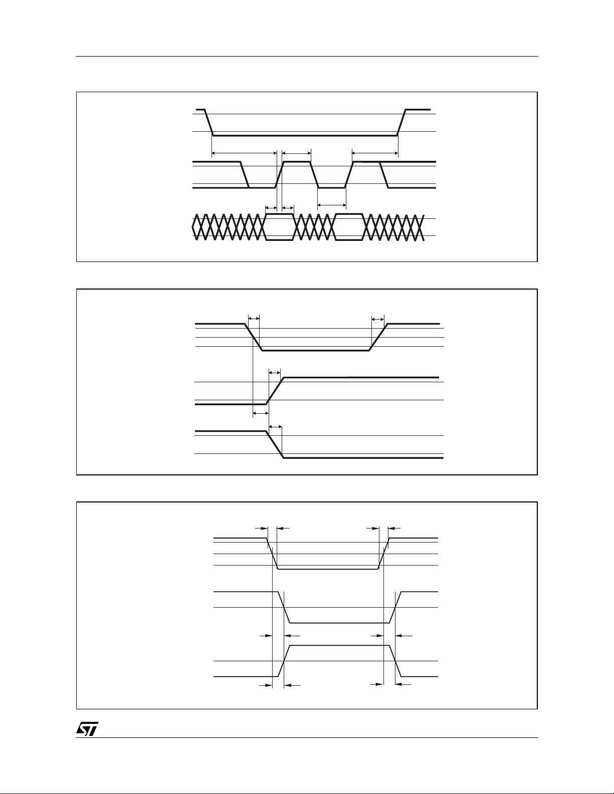
Figure 9. SPI-interface - Input Timing
L9949
CSN
t
set CSN
t
CLKH
CLK
t
CLKL
V alid
DI
t
set DI
V alid
t
hold DI
Figure 10. Data Out Valid Data Delay Time and Valid Time
t
f in
CLK
t
r DO
DO
(low to high)
t
d DO
t
f DO
DO
(high to low)
t
set CLK
t
0.8 V
CC
0.2 V
CC
0.8 V
CC
0.2 V
CC
0.8 V
CC
0.2 V
CC
r in
0.8 V
CC
0.5 V
CC
0.2 V
CC
0.7 V
CC
0.3 V
CC
0.7 V
CC
0.3 V
CC
Figure 11. SPI-Interface - Data Out Enable and Disable Time
t
f in r in
CSN
DO
pull-up load to V
CL =100pF
pull-down load to GND
C
=100pF
L
DO
CC
t t
en DO tri L
t
en DO tri H
t
dis DO L tri
t
dis DO H tri
0.8 V
50%
0.2 V
50%
50%
CC
CC
17/20

L9949
t
t
F
e
e
t
Figure 12. SP I-I nte rfa ce - Driver Turn On/O ff Tim i ng
CSN low to high: data fro m shift register
is
ransferred to output pow er sw itc he s
t
r in
CSN
t
dOFF
output current
of a driv
r
output current
of a driv
r
ON sta
eO
OFF
OFF state
t
dON
t
ON
F state
ON state
Figure 13. SP I-Interface - Timin g of Status Bit 0 (Fa ul t Co nd ition)
CSN high to low and CLK stays low: status information of data bit 0 (fault condition) is transfered to Data Out
t
f in
80%
50%
20%
80%
50%
20%
80%
50%
20%
18/20
CSN
CLK
DI
DO
Data In: data is not accepted
0
-
Data Out: status information of data bit 0 (fault condition) will stay as long as CSN is low
time
time
time
time

L9949
DIM.
MIN. TYP. MAX. MIN. TYP . MAX.
mm inch
A 3.6 0.142
a1 0.1 0.3 0.004 0.012
a2 3.3 0.130
a3 0 0.1 0.000 0.004
b 0.4 0.53 0.016 0.021
c 0.23 0.32 0.009 0.013
D (1) 15.8 16 0.622 0.630
D1 9.4 9.8 0.370 0.386
E 13.9 14.5 0.547 0.570
e 1.27 0.050
e3 11.43 0.450
E1 (1) 10.9 11.1 0.429 0.437
E2 2.9 0.114
E3 5.8 6.2 0.228 0.244
G 0 0.1 0.000 0.004
H 15.5 15.9 0.610 0.626
h 1.1 0.043
L 0.8 1.1 0.031 0.043
N 8˚ ( typ.)
S 8˚ (max. )
T 10 0.394
(1) “D and E1” do not include mold flash or protusions.
- Mold flash or protusions shall not exceed 0.15m m (0. 006”)
- Critical dimensions: “E”, “G” and “a3”.
OUTLINE AND
MECHANICAL DA TA
Weight:
1.9gr
JEDEC MO-166
PowerSO20
E2
NN
a2
b
h x 45
DETAIL A
e3
H
D
T
110
e
1120
E1
A
DETAIL B
PSO20MEC
R
lead
a3
Gage Plane
BOTTOM VIEW
E
DETAIL B
0.35
S
D1
L
c
a1
DETAIL A
slug
- C -
SEATING PLANE
GC
(COPLANARITY)
E3
0056635
19/20

L9949
Information furnished is believed to be accurate and reliable. However, STMicroelectronics assumes no responsibility for the consequences
of use of such information nor for any infringement of patents or other rights of third parties which may result from its use. No license is granted
by implic ation or otherwise under any patent or patent r i ght s of STMi croelectr oni cs. Spec i fications mentioned i n this publication are s ubj ect
to change without notice. This publication supersedes and replaces all information previously supplied. STMicroelectronics product s are not
authorized for use as cri tical comp onents in lif e support devi ces or systems without express written approva l of STMicroel ectronics.
The ST logo is a registered trademark of STMicroelectronics
© 2002 STMic roelectroni cs - All Rig hts Reserved
Austra lia - Brazil - Canada - Chi na - F i nl and - Franc e - Germany - Hong Kong - In di a - Israel - Ita l y - J apan -Malaysia - Malta - Morocco -
Singap ore - Spain - Sw eden - Switze rl and - Unit ed K i ngdom - United States .
STMicroelectronics GROUP OF COMPANIES
http://www.s t. com
20/20
 Loading...