

®
DMOS DUAL FULL BRIDGE DRIVER
2 INDE P E NDE N T LY C O NTROLLED
H-BRIDGES
DS,ON
R
<0.9Ω @ T
0.8A DC CURRENT WITHOUT HE AT S I NK
LOW QUIESCENT MODE Iq <200µA
THEMAL PROTECTION
CROSS CONDUCTION PROTECTION
SUPPLY VOLTAG E UP TO 40V
CMOS COMPATIBLE INPUTS
OUTPUT SHORT-CIRCUIT PROTECTION
amb
= 25°C, VS = 14V
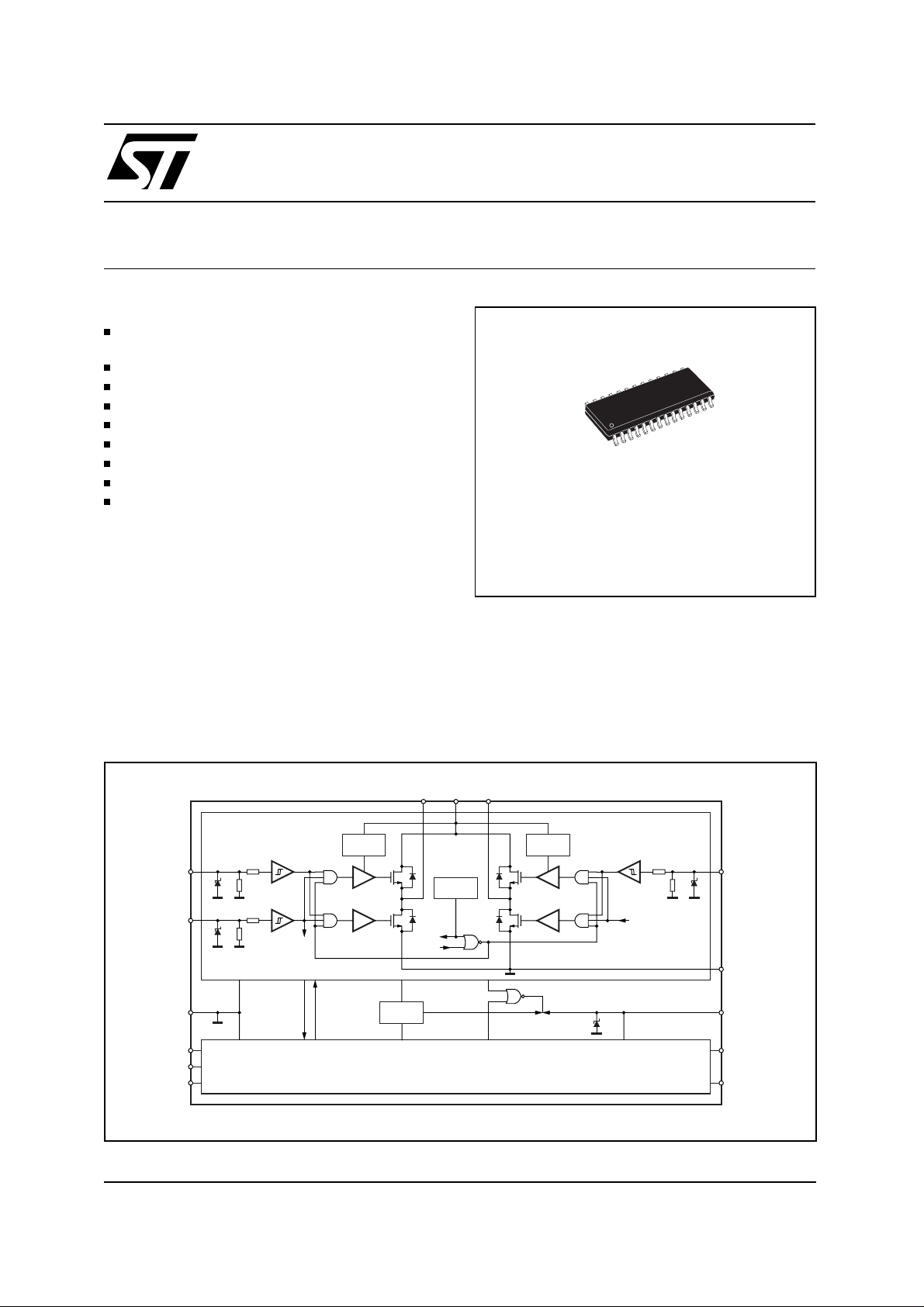
L9925
SO28
DESCRIPTION
The L9925 is a dual full bridge driver for stepper
motor applications. Realized in BCD (Bipolar,
CMOS & DOS) techology, logic circuits, precise
linear blocks and power transistors are combined
to optimize circuit performance and minimize off
chip components. Schmitt triggers are used for all
input stages and are fully compatible with 5V
CMOS logic levels. When both enable signals are
low, the IC is commanded to a low quiescent current state and will draw less than 200µA from the
battery.
BLOCK DIAGRAM
OUT1 VS1 OUT2
CHARGE
PUMP
IN1
EN1
7V T1
1st FULL BRIDGE
EN1
T1T2T2
ORDERING NUMBER: L9925
The charge pump is integrated on chip; no external components are required. Full performance is
S
maintaned for 9V <V
S
6V <<V
<9V and 16V <VS <40V yields full func-
<16V. Extended ranges of
tionally but with relaxed performance. Over temperature protection and ESD protection to all pins
ensures relability and reduces system integration
failures.
CHARGE
PUMP
IN2
TEMP
EN1
EN1
7V7V
PGND1
GND
EN2
IN3
IN4
2nd FULL BRIDGE
T1 T2
5V
REGULATOR
40V
EN2
D99AT423
VS2
OUT3
OUT4
March 1999
....... ................................. ........................................ ................................. ...................... ........................................ ................................
1/9
L9925
ABSOLUTE MAXIMUM RATINGS
Absolute Maximum Ratings are those values bey ond whih dam age to the device may occur. Functional
operation under these condition isn’t implied.
For voltages and currents applied externally to the device:
Symbol Parameter Value Unit
V
VSDC
V
VSP
I
OUT
I
OUT MAX
V
IN1,2
V
EN
T
, T
stg
P
tot
(1) Device may be overstressed if pulsed simultaneous with short circ ui t at one or more of the outputs will be present.
Dc Supply Voltage -0.3 to 26 V
Supply Voltage Pulse (T ≤400ms)
DC Output Load Current
DC Output Current: for VOUT > VVS +0.3V or VOUT < -0.3V
(1)
40 V
1.2 A
±
1.8 A
±
the internal DMOS reverse and/or substrate diode become
conductive and the applied current should not exceed the
specified limit.
DC Input Voltage -0.3 to 7 V
Enable Input Voltage -0.3 to 7 V
Storage and Junction Temperature -40 to 150 °C
j
Total Power Dissipation (T
(T
(T
= 80°C)
pins
= 70°C no copper area on PCB)
amb
=70°C 8 cm2 copper area on PCB)
amb
5
1.23
2
W
W
W
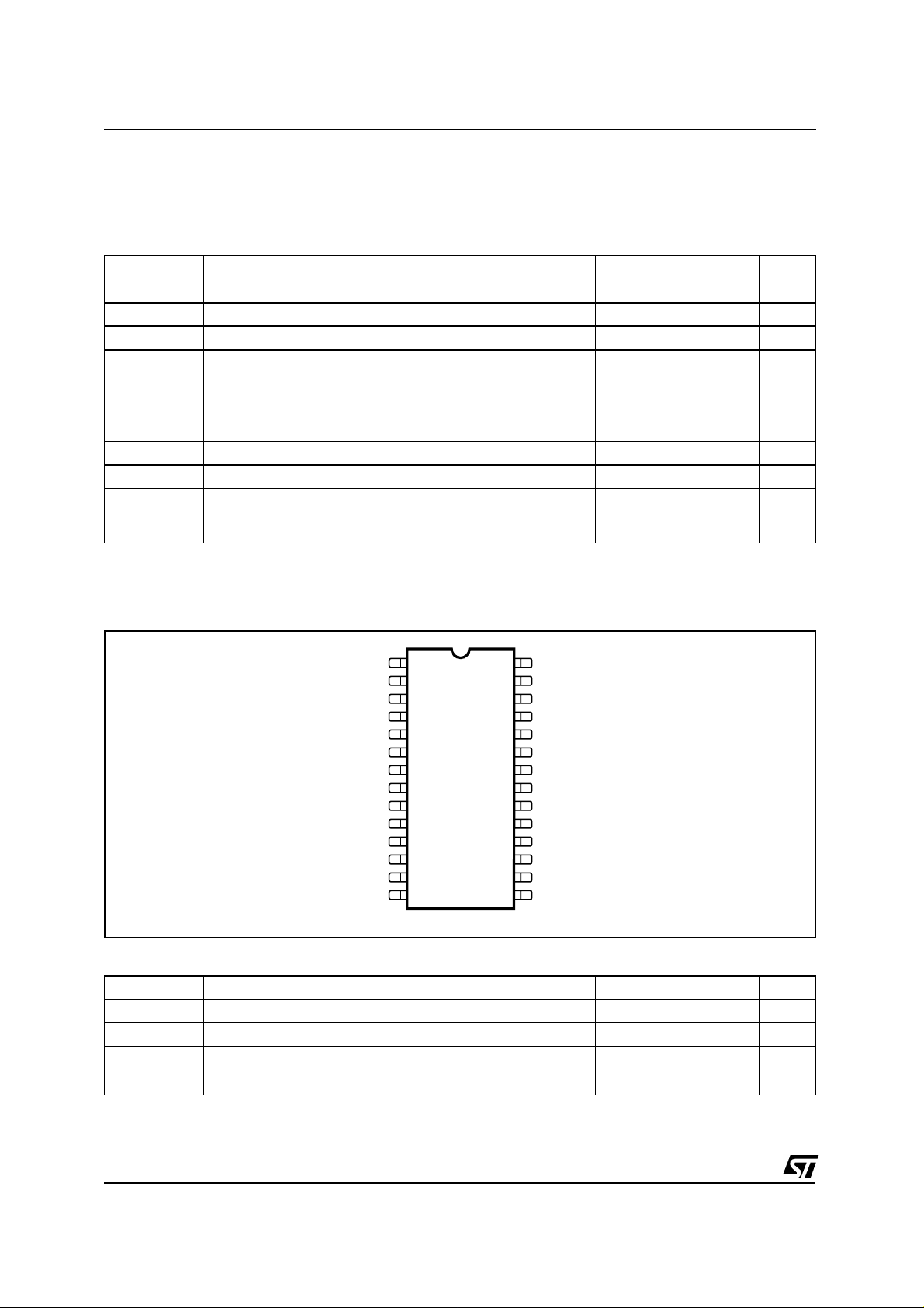
PIN CONNECTION
PGND
IN1
EN1
N.C.
N.C.
OUT1
GND
GND
OUT3 VS2
N.C. N.C.
N.C.
EN2
IN3 IN4
2
3
4
5
6
7
8
9
10
12
13
D88AT424
28
27
26
25
24
23
22
21
20
19
18
17
16
1514PGND N.C.
N.C.1
IN2
OUT2
N.C.
N.C.
VS1
GND
GND
N.C.11
OUT4
THERMAL DATA
Symbol Parameter Value Unit
T
jTS
T
jTSH
R
th j-amb
R
th j-pins
(2)
With 6cm2 on board heat sink area
Thermal Shut-down junction temperature min. 150 °C
Thermal Shut-down thereshold hysteresis typ. 25 °C
Thermal Resistance Junction-ambient
(2)
50 °C/W
Thermal Resistance Junction-pins 15 °C/W
2/9

PIN FUNCTIONS
N. Name Function
1 PGND1 Ground for DMOS sources in bridge 1
2 IN1 Digital Input from motor controller for bridge 1
3 EN1 Logic enable/disable for bridge 1 (active high)
4, 5 NC No connect
6 OUT1 Output of one half of bridge 1
7, 8 GND Ground
9 OUT3 Output of one half of bridge 2
10, 11 NC No connect
12 EN2 Logic enable/disable for bridge 2 (active high)
13 IN3 Digital Input from motor controller for bridge 2
14 PGND2 Ground for DMOS sources in bridge 2
15 NC No connect
16 IN4 Digital Input from motor controller for bridge 2
17 OUT4 Output of one half of bridge 2
18, 19 NC No connect
20 VS2 Supply Voltage for bridge 2
21, 22 GND Ground
23 VS1 Supply Voltage for bridge 1
24, 25 NC No connect
26 OUT2 Output of one half of bridge 1
27 IN2 Digital Input from motor controller for bridge 1
28 NC No connect
L9925
ELECTRICAL CHARACTERISTICS
S
= 9 to 16V; Tj = -40 to 150°C
(V
(3)
, unless otherwise specified.)
Symbol Parameter Test Condition Min. Typ. Max. Unit
T
T
T
R
d-on
d-SB
d-off
t
rise
t
IL
I
S
ds
fall
Quiescent Current EN1 = EN2 =0V; Tj = 85°C 200
EN1 = EN2 =5V; I
= 0A 5 12 mA
load
Switch on Resistance Tj = 25°C; VS = 14V; Io =300mA 0.75 0.8
T
= 125°C; VS = 6V; Io =300mA 1.5 1.9
j
Turn-on delay See Fig 1 10 50
Standby setting time See Fig 1 50 200
Turn-off delay See Fig 1 10 50
Output rise time (10 to 90%) See Fig 1 0.5 5 20
Output fall time (90 to 10%) See Fig 1 0.5 5 20
Output leakage current EN = 0V; Vo =VS or GND -10 10 mA
o
INx, ENx Logic Input Low voltage -0.3 1.5 V
Logic Input High voltage 3.5 6 V
Hysteresis 0.5 1.0 2.0 V
Ibias Input bias current -50 300
The voltage refered to GND and currents are assumed positive, when the current flows into the pin.
(3) Tested up to 125°C, parameter guaranted by correlation up to 150°C
A
µ
Ω
Ω
s
µ
s
µ
s
µ
s
µ
s
µ
A
µ
3/9
 Loading...