

■
OPERATING SU PPLY VOLTAGE 8V TO 28V,
OVERVOLTAGE MAX. 40V
■
OPER ATING SUPPLY VOLTAGE 6V WITH
IMPLEMENTED STEPUP CONVERTER
■
QUIESCENT CURRENT IN STANDBY MODE
LESS THAN 50µA
■
ISO 9141 COMPATIBLE INTERFACE
■
CHARGE PUMP FOR DRIVING A POWER
MOS AS REVERSE BATTERY PROTECTION
■
PWM OPERATION FREQUENCY UP TO
30KHZ
■
PROGRAMMABLE CROSS CONDUCTION
PROTECTION TIME
■
OVERVOLTAGE, UNDERVOLTAGE, SHORT
CIRCUIT AND THERMAL PROTECTION
■
REAL TIME DIAGN OS TIC
L9904
MOTOR BRIDGE CONTROLLER
PRODUCT PREVIEW
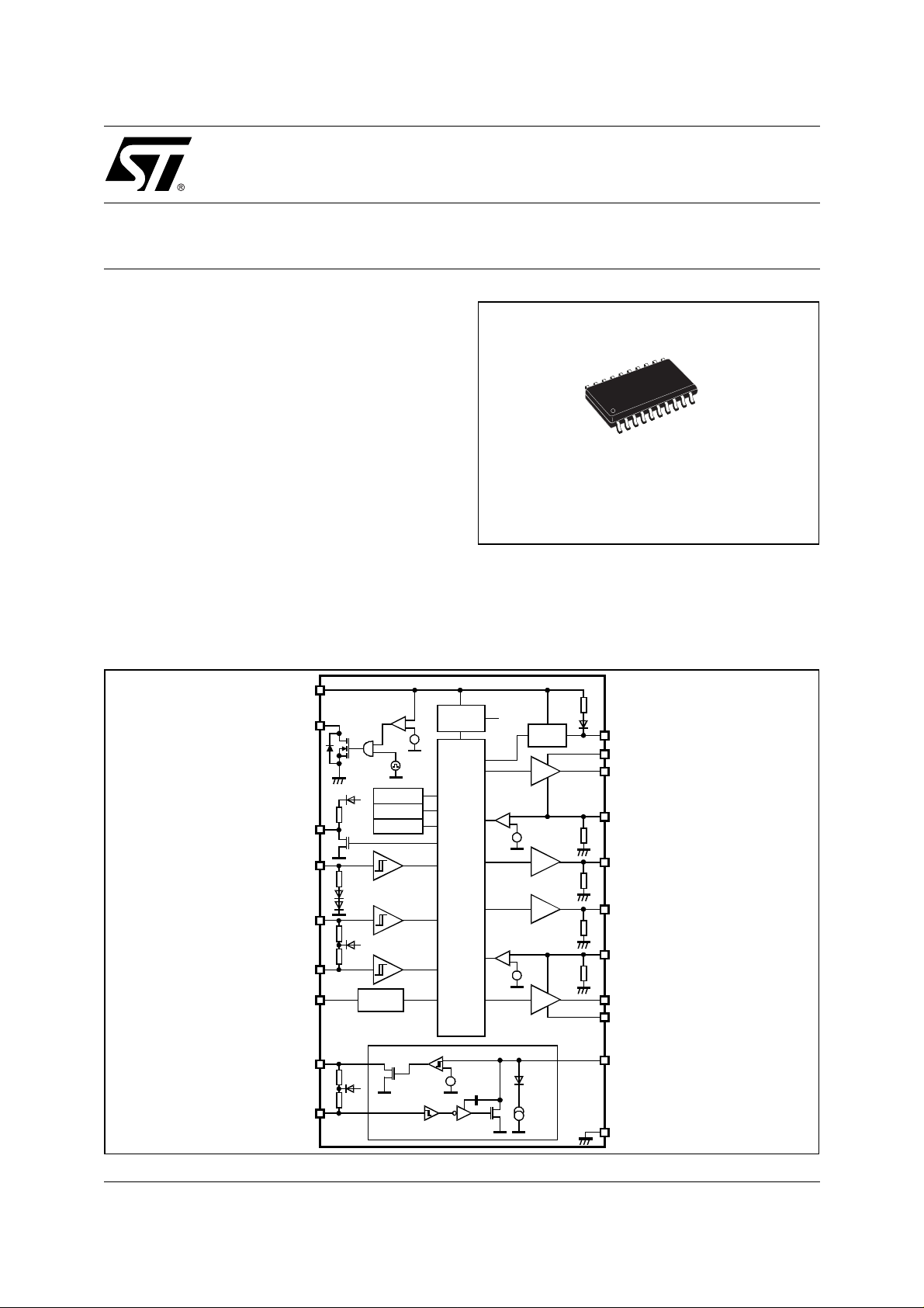
SO20
ORDERING NUMBER: L9904
DESCRIPTION
Control circuit for power MOS bridge driver in automotive applications with ISO 9141bus interface.
BLOCK DIAGRAM
PWM
DIR
10
VS
R
Reference
=
V
STH
f
ST
ISO-Interface
=
VCC
VCC
+
Overvolt age
Undervo ltage
Thermal shutdown
Timer
1
ST
R
DG
2
DG
4
EN
R
EN
5
R
DIR
R
PWM
3
6
PR
7
RX
R
RX
VCC
R
TX
8
TX
BIAS
0.5 • V
VCC
Charge
pump
=
V
S1TH
Control L ogi c
=
V
S2TH
VS
I
KH
CP
11
CP
13
CB1
12
GH1
14
S1
R
S1
19
GL1
R
GL1
18
GL2
R
GL2
17
S2
R
S2
15
GH2
16
CB2
9
K
20
GND
October 2002
This is preliminary information on a new product now in development. Details are subject to change without notice.
1/17
L9904
PIN FUNCTION
N° Pin Description
1 ST Open Drain Switch for Stepup converter
2 DG Open drain diagnostic output
3 PWM PWM input for H-bridge control
4 EN Enable input
5 DIR Direction select input for H-bridge control
6 PR Programmable cross conduction protection time
7 RX ISO 9141 interface, receiver output
8 TX ISO 9141 interface, transmitter input
9 K ISO 9141 Interface, bidirectional communication K-line
10 VS Supply voltage
11 CP Charge pump for driving a power MOS as reverse battery protection
12 GH1 Gate driver for power MOS highside switch in halfbridge 1
13 CB1 External bootstrap capacitor
14 S1 Source/drain of halfbridge 1
15 GH2 Gate driver for power MOS highside switch in halfbridge 2
16 CB2 External bootstrap capacitor
17 S2 Source/drain of halfbridge 2
18 GL2 Gate driver for power MOS lowside switch in halfbridge 2
19 GL1 Gate driver for power MOS lowside switch in halfbridge 1
20 GND Ground
PIN CONNECTION
2/17
(Top view)
ST
DG
PWM
EN
DIR
PR
RX
TX
K GH1
VS CP
2
3
4
5
6
7
8
9
10
SO20
20
19
18
17
16
15
14
13
12
11
GND1
GL1
GL2
S2
CB2
GH2
S1
CB1

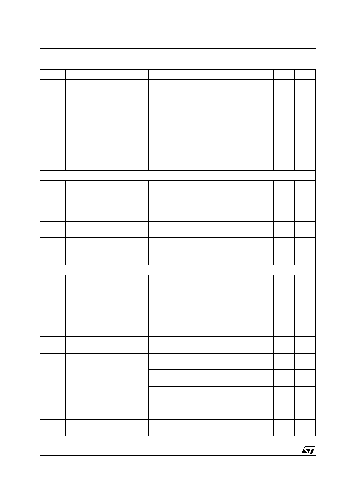
ABSOLUTE MAXIMUM RATINGS
Symbol Parameter Value Unit
V
I
CB1
CB1
, V
, I
Bootstrap voltage -0.3 to 40 V
CB2
Bootstrap current -100 mA
CB2
L9904
V
I
CP
V
DIR
,V
PWM ,VTX
I
DIR
,I
PWM ,ITX
VDG ,V
CP
,V
,I
Charge pump voltage -0.3 to 40 V
Charge pump current -1 mA
Logic input voltage -0.3 to 7 V
EN
Logic input current ±1 mA
EN
Logic output voltage -0.3 to 7 V
RX
IDG ,IRX Logic output current -1 mA
V
GH1
I
GH1
V
GL1
I
GL1
V
VS1 , V
, V
, I
V
I
PR
, V
, I
PR
Gate driver voltage -0.3 to VSX + 10 V
GH2
Gate driver current -1 mA
GH2
Gate driver voltage -0.3 to 10 V
GL2
Gate driver current -10 mA
GL2
K-line voltage -20 to V
K
S
Programming input voltage -0.3 to 7 V
Programming input current -1 mA
Source/drain voltage -2 to VVS + 2 V
S2
V
I
S1
V
, I
V
ST
I
ST
VSDC
V
VSP
I
VS
Source/drain current -10 mA
S2
Output voltage -0.3 to 40 V
Step up output current -1 mA
DC supply voltage -0.3 to 28 V
Pulse supply voltage (T < 500ms) 40 V
DC supply current -100 mA
For externally applied voltages or currents exceeding these limits damage of the device may occur!
All pins of the IC are protected against ESD. The verification is performed according to MIL883C, human body
Ω
model with R=1.5k
, C=100pF and discharge voltage ±2kV, cor responding to a max imum dis charge ener gy of
0.2mJ.
3/17
L9904
THERMAL DATA
Symbol Parameter Value Unit
T
T
JSD
T
JSDH
R
th j-amb
1. see application note 110 for SO packa ges.
ELECT RICAL CH ARACTER ISTCS
Operating junction temperature -40 to 150 °C
J
Junction temperature thermal shutdown threshold min 150 °C
Junction thermal shutdown hysteresis typ 15 °C
Thermal resistance junction to ambient
1)
85 °C/W
(8V < VVS < 20V, VEN = HIG H, -40 °C ≤ TJ ≤ 150°C, unless otherwise spec-
ified. The voltages are refered to GND and currents are assumed positive, when current flows into the pin.
Symbol Parameter Test Condition Min. Typ. Max. Unit
Supply (VS)
V
VS OVH
Overvoltage disable HIGH
threshold
V
VS OVh
V
VS UVH
Overvoltage threshold hysteresis
Undervoltage disable HIGH
threshold
V
VS UVh
I
VSL
I
VSH
I
VSD
Undervoltage threshold
hysteresis
2)
Supply current VEN = 0 ; VVS = 13.5V; TJ< 85°C 50 µA
Supply current, pwm-mode VVS= 13.5V; VEN= HIGH;
Supply current, dc-mode VVS= 13.5V; VEN= HIGH;
Enable input (EN)
V
V
V
R
Low level 1.5 V
ENL
High level 3.5 V
ENH
ENh
Hysteresis threshold
Input pull down resistance VEN = 5V 16 50 100 kΩ
EN
2)
H-bridge control inputs (DIR, PWM)
V
V
PWML
V
DIRH
V
PWMH
V
V
PWMh
DIRL
DIRh
Input low level 1.5 V
Input high level 3.5 V
Input threshold hysteresis
2)
V
= LOW; S1 = S2 = GND
DIR
f
= 20kHz; C
PWM
= 4.7nF; C
C
GLX
R
= 10kΩ; C
PR
V
= LOW; S1 = S2 = GND
DIR
V
= LOW; C
PWM
= 10kΩ; C
R
PR
2)
CBX
GHX
= 150pF
PR
GHX
= 150pF
PR
= 0.1µF;
= 4.7nF;
= 4.7nF
28 33 36 V
1.6 V
67V
0.66 V
8.1 13 mA
5.8 10 mA
1V
1V
4/17
L9904
ELECTRICAL CHARACTERISTICS
(continued)
Symbol Parameter Test Condition Min. Typ. Max. Unit
R
R
PWM
Internal pull up resistance
DIR
to internal VCC
V
= 0; V
3)
DIR
= 0 16 50 100 kΩ
PWM
DIAGNOSTIC output (DG)
V
R
Programmable cross conduction protection
N
I
Output drop IDG = 1mA 0.6 V
DG
Internal pull up resistance
DG
to internal VCC
Threshold voltage ratio V
PR
V
PRL
Current capability
PR
3)
PRH
VDG = 0V 10 20 40 kΩ
4)
R
V
PR
PR
= 10kΩ
= 2V
1.8 2 2.2
-0.5 mA
/
ISO interface, transmission input (TX)
V
V
V
R
Input low level 1.5 V
TXL
Input high level 3.5 V
TXH
Input hysteresis voltage 2) 1 V
TXh
Internal pull up resistance to
TX
VTX = 0 10 20 40 kΩ
internal VCC 3)
ISO interface, receiver output (RX)
V
RXL
R
RX
R
RXON
t
RXH
t
RXL
Output voltage high stage
Internal pull up resistance
to internal VCC
3)
TX = HIGH; IRX = 0; V
TX = HIGH;
= 0V
V
RX
ON resistance to ground TX = LOW;
= 1mA
I
RX
Output high delay time Fig. 1 0.5 µs
Output low delay time 0.5 µs
= V
K
VS
4.5 5.5 V
51020kΩ
40 90 Ω
ISO interface, K-line (K)
R
V
V
V
I
I
KSC
Input low level -20V 0.45 ·
KL
Input high level
KH
Input hysteresis voltage 2) 0.025·
Kh
Input current VTX = HIGH -5 25 µA
KH
ON resistance to ground VTX = LOW; IK=10mA 10 30 Ω
KON
0.55 ·
V
VS
V
VS
Short circuit current VTX = LOW 40 130 mA
f
Transmission frequency 60 100 kHz
K
2. not tested in production: guaranteed by design and veri fied in charac terization
3. Internal V
4. see page 18 fo r calculation of programmable cross conduction protection time
is 4.5V ... 5.5V
VCC
V
VS
V
VS
0.8V
5/17
L9904
ELECTRICAL CHARACTERISTICS
(continued)
Symbol Parameter Test Condition Min. Typ. Max. Unit
t
Rise time VVS = 13.5V; Fig. 1
Kr
26µs
External loads at K-line:
= 510Ω pull up
R
K
to V
VS
C
= 2.2nF to GND
K
t
Fall time 26µs
Kf
t
t
t
Switch high delay time 4 17 µs
KH
Switch low delay time 4 17 µs
KL
Short circuit detection time VVS = 13.5V;
SH
10 40 µs
TX = LOW
> 0.55 · V
V
K
VS
Charge pump
V
I
t
Charge pump voltage VVS = 8V
CP
Charging current
CP
CP
= VVS + 8V
V
CP
Charging time
2)
VCP= VVS + 8V
= 13.5V
V
VS
= 20V
V
VS
V
= 13.5V -50 -75 µA
VS
V
= 13.5V
VS
C
= 10nF
CP
V
7V
V
10V
V
10V
VS
VS
VS
+
+
+
1.2 4 ms
VVS+
14V
V
VS
14V
V
VS
+14V
+
f
Charge pump frequency VVS = 13.5V 250 500 750 kHz
CP
Drivers for external highside power MOS
V
V
R
R
R
GH1H
R
GH2H
V
GH1H
V
GH2H
R
R
R
R
GH1L
GH2L
Bootstrap voltage VVS = 8V; I
CB1
CB2
ON-resistance of SINK stage
ON-resistance of SOURCE stage I
Gate ON voltage (SOURCE) VVS= VSX = 8V; I
Gate discharge resistance EN = LOW 10 100 kΩ
GH1
GH2
Sink resistance 10 100 kΩ
S1
S2
VVS =13.5V; I
VVS = 20V; I
V
CBX
I
GHX
V
CBX
I
GHX
GHX
I
GHX
C
CBX
V
= VSX = 13.5V; I
VS
C
CBX
V
= VSX = 20V; I
VS
C
CBX
CBX
CBX
CBX
= 8V; VSX = 0
= 50mA; T
= 8V; VSX = 0
= 50mA; T
= -50mA; TJ = 25°C
= -50mA; TJ = 125°C
= 0.1µF
= 0.1µF
= 0.1µF
= 0; VSX = 0
= 0; VSX = 0
= 0; VSX = 0
= 25°C
J
= 125°C
J
= 0;
GHX
= 0;
GHX
= 0;
GHX
7.5
10
10
V
VS
+6.5V
VVS+
10V
V
VS
+10V
14
14
14
10 Ω
20 Ω
10
20
V
VS
+14V
V
VS
+14V
V
VS
+14V
V
V
V
Ω
Ω
6/17

L9904
ELECTRICAL CHARACTERISTICS
(continued)
Symbol Parameter Test Condition Min. Typ. Max. Unit
Drivers for external lowside power MOS
R
GL1L
R
GL2L
R
GL1H,
R
GL2H
V
GL1H,
V
GL2H
R
R
2. not tested in producti on: guaranteed by design an d verified in characterizat i on
ON-resistance of SINK stage I
ON-resistance of SOURCE stage I
Gate ON voltage (SOURCE) VVS = 8V; I
Gate discharge resistance EN = LOW 10 100 kΩ
GL1
GL2
= 50mA; TJ = 25°C
GLX
I
= 50mA; TJ = 125°C
GLX
= -50mA; TJ = 25°C
GLX
I
= -50mA; TJ = 125°C
GLX
= 0
V
VS
VVS = 20V; I
GLX
= 13.5V; I
GLX
GLX
= 0
= 0
7V
10V
10V
10
20
10
20
V
VS
V
VS
14V
Timing of the drivers
t
GH1LH
t
GH2LH
Propagation delay time Fig. 2
V
VS
= 13.5V
500 ns
VS1 = VS2 =0
C
= 0.1µF
CBX
RPR= 10kW
t
GH1LH
t
GH2LH
t
GH1HL
t
GH2HL
Propagation delay time including
cross conduction protection time
t
CCP
Propagation delay time 500 ns
Fig. 2
= 13.5V
V
VS
VS1 = VS2 =0
C
= 0.1µF
CBX
= 150pF;
C
PR
0.7 1 1.3 µs
RPR= 10kΩ;
5)
t
GL1LH
t
GL2LH
Propagation delay time Fig. 2
V
VS
V
S1
C
CBX
= 13.5V
= VS2 =0
= 0.1µF
500 ns
Ω
Ω
Ω
Ω
t
GL1LH
t
GL2LH
t
GL1HL
t
GL2HL
t
GH1r
t
GH2r
t
GH1f
t
GH2f
t
GL1r
t
GL2r
t
GL1f
t
GL2f
= 10kΩ
R
PR
Propagation delay time including
cross conduction protection time
t
CCP
Propagation delay time 500 ns
Fig. 2
= 13.5V
V
VS
VS1 = VS2 =0
C
= 0.1µF
CBX
= 150pF;
C
PR
R
= 10kΩ;
PR
0.7 1 1.3 µs
5)
Rise time Fig. 2
= 13.5V
V
VS
V
= VS2 =0
Fall time 1µs
Rise time 1µs
C
C
C
S1
CBX
GHX
GLX
= 0.1µF
= 4.7nF
= 4.7nF
1µs
RPR= 10kΩ;
Fall time 1µs
7/17

L9904
ELECTRICAL CHARACTERISTICS
(continued)
Symbol Parameter Test Condition Min. Typ. Max. Unit
Short Circuit Detection
V
S1TH
V
S2TH
t
SCd
Step up converter (ST) (5.2V ≤ V
V
V
R
DSON
f
Threshold voltage 4 V
Detection time 5 10 15 µs
< 10V)
VS
ST disable HIGH threshold 10 V
STH
ST disable threshold hysteresis
STh
voltage
Open drain ON resistance
Clock frequency 50 100 149 kHz
ST
2. not tested in productio n: g uaranteed by des i gn and verified in characterization
5. tested wit h di ffered values in producti on but guaran teed by design and verified in characterization
2)
= 5.2V;
V
VS
= 50mA
I
ST
12V
20 Ω
8/17

Figure 1. Timin g of the IS O-interface
V
TX
0.3 • V
VCC
t
V
K
KL
t
Kf
0.7 • V
t
KH
t
Kr
VCC
0.3 • V
L9904
VCC
t
0.55 • V
0.45 • V
V
open drain
transistor at
K-pin
ON
OFF
RX
VS
VS
t
RXL
0.3 • V
VCC
20%
80%
t
RXH
0.7 • V
VCC
IK> I
t
SH
KSC
Figure 2. Tim in g of t he dri v ers for the external MOS regard in g t he in puts DIR and PWM
PWM
or
DIR
50%
t
t
GHX
GLX
80%
20%
80%
20%
t
GHXLHtGHXr
t
GLXHLtGLXf
t
GHXHL
t
GLXLH
t
GHXf
t
GLXr
t
t
t
9/17

L9904
g
y
(
y
gy
Figure 3. I(V) characteristics of the K-Line for TX = HIGH and VVS=13.5V
IK [mA]
0.2
Figure 4. Dri vin g s equence
0.1
0.0
-0.1
-0.2
-0.3
-0.4
-0.5
-20 -10 0 10 20
Ω
~50k
VK [V]
EN
Ω
~50k
≈
Note:
Befo r e standb
mode
EN=low) a braking phase
is mandator
the stored ener
to discharge
of the
motor.
DIR
PWM
GL2
GH2
GL1
GH1
≈
brakin
≈≈
≈
10/17

L9904
Figure 5. Charging time of an external capacitor of 10nF connected to CP pin at VVS=8V and
VVS=13.5V
voltage [V]
30
25
20
15
10
5
0
01234
Figure 6. Application Circuit Diagram
V
BAT
D1
VS
10
C
C
S2
Voltage
Regulator
µC
V
GND
CC
S1
ST
1
VCC
Overv oltage
Undervo ltage
R
DG
DG
EN
DIR
PWM
PR
C
R
PR
PR
RX
TX
Thermal shut down
2
4
R
EN
5
R
DIR
VCC
R
PWM
3
6
Timer
7
R
RX
VCC
R
TX
8
Charging time of a 10nF load at CP
CP for VS=13.5V
CP for VS=8V
EN
time [ms]
R
Reference
+
V
=
STH
f
ST
VCC
BIAS
Charge
pump
V
=
S1TH
Control Logic
V
=
S2TH
ISO-Interface
0.5•V
=
VS
I
KH
CP
CP
11
CB1
13
GH1
12
S1
14
R
S1
GL1
19
R
GL1
GL2
18
R
GL2
S2
17
R
S2
GH2
15
CB2
16
K
9
GND
20
R
C
B1
C1
M
R
R
C
B2
R
K-Line
11/17

L9904
FUNCTIONAL DESCRIPTION
General
The L9904 integrated circuit (IC) is designed to control four external N-channel MOS transistors in H-Bridge configuration for DC-motor driving in automoti ve application s. It includes an ISO9141 compatibl e interface. A typical
application is shown in fig.6.
Voltage supply
The IC is supplied via an external reverse battery protection diode to the VVS pin. The typical operating voltage
range is down to 8V.
The supply current consumption of the IC composes of static and a dynamic part. The static current is typically
5.8mA. The dynamical current I
of the external power mos transistor. The current can be estimated by the expression:
An external power transistor with a gate charge of Q
quires a dynamical supply current of I
The total supply current consumption is I
Extended supply voltage range (ST)
The operating battery voltage range can be extended down to 6V using the additional components shown in
fig.7. A small inductor of L~150µH (I
with the switching open drain output ST. The switching frequency is typical 100kHz with a fixed duty cycle of
50%. The step up converter starts below V
at V
> 10V to avoid EME at nominal battery voltage. The diode D2 in s eries w ith the ST pin is neces sar y onl y
VS
for systems with negative battery voltage. No additional load can be driven by the step up converter.
is depending of the PWM frequency f
dyn
= 2 · f
I
dyn
= 6.4mA.
dyn
= 5.8mA + 6.4mA = 12.2mA.
VS
~500mA) in series to the battery supply builts up a step up converter
peak
< 8V, increases the supply voltage at the VS pin and switches off
VS
· Q
PWM
Gate
Gate
= 160nC and a PWM frequency of f
and the required gate charge Q
PWM
PWM
Gate
= 20kHz re-
Figure 7.
V
BAT
L1 D1
D2
C1 C2
VS
ST
L9904
-
+
V
=
STH
f
ST
12/17

L9904
FUNCTIONAL DESCRIPTION
(continued)
Control inputs (EN, DIR, PWM)
The cmos level inputs drive the device as shown in fig.4 and described in the truth table.
The device is ac tivated with ena ble input HIGH si gnal. For enable input fl oating (not c onnected) or VE N=0V the
device is in standby mode. When activating the device a w ake-up time of 50µs is recommended to stabilize the
internal supplies.
The DIR and PWM inputs control the driver of the external H-Bridge transistors. The motor direction can be
choosen with the DIR input, the duty cycle and frequency with the PWM input. Unconnected inputs are defined
by internal pull up resistors. D uring wak e-up and braking and befor e dis activ ating the IC via enable both i nputs
should be driven HIGH.
Truth table:
Status Control inputs Device status
EN DIR
1 0xxxxxxRRRR T standby mode
2 1xx1000LLLL L thermal
3 1xx0100LLLL L overvoltage
4 1xx0010LLLL L undervoltage
PWM
TS OV UV SC GH1 GL1 GH2 GL2 DG
Driver stage for external
power MOS
Diagnostic Comment
shutdown
6)
6)
6)
5 1xx0001
6 1000000LHHL H
7 1x10000LHLH H braking mode
8 1100000HLLH H
X
X
X
6
X
L
short circuit
Symbols: x Don't care R:Resistive output TS:Thermal shutdown
0: Logic LOW or not active L: Output in sink condition OV:Overvoltage
1: Logic HIGH or active H: Output in source condition UV:Undervoltage
T: Tristate SC:Short Circuit
6. Only those external MOS transistors of the H-Bridge which are in short circuit condition are switched off. All others remain driven
by DIR and PWM.
Thermal shutdown
When the junction temperature exceeds T
the diagnostic DG is LOW until the junction temperature drops below T
all driver are switched in si nk condition ( L), the K- output is off and
JSD
JSD
- T
JHYST
.
Overvoltage Shutdown
When the supply voltage VVS exceeds the overvoltage threshold V
all driver are switched in sink condi-
VSOVH
tion (L), the K- output is off and the diagnostic DG is LOW.
6)
13/17

L9904
FUNCTIONAL DESCRIPTION
Undervoltage Shutdown
(continued)
For supply voltages below the undervoltage disable threshold the gate driver remains in sink condition (L) and
the diagnostic DG is low.
Short Circuit Detection
The output voltage at the S1 and S2 pin of the H-Bridge is monitored by comparators to detect shorts to ground
or battery. The activated ex ternal highside MOS transistor will be s witched off i f the vol t age drop remai ns below
the comparator threshold voltage V
S1TH
and V
for longer than the short current detection time t
S2TH
SCd
. The
transistor remains in off condition, the diagnostic output goes LOW until the DIR or PWM input status will be
changed. The status doesn' t chang e for the other MOS transis tors. The exter nal lowside MOS tr ansi stor will be
switched off if the voltage drop passes over the comparator threshold voltage V
the short current detection time t
. The transistor remains in off condition, the diagnostic output goes LOW
SCd
S1TH
and V
for longer than
S2TH
until the DIR or PWM input status will be changed. The status doesn't change for the other MOS transistors.
Diagnostic Output (DG)
The diagnostic output provides a real time error detection, if monitors the following error stacks: Thermal shutdown, overvoltage shutdown , undervoltage shutdown and short circuit shutdown. The open drain output with
internal pull up resistor is LOW if an error is occuring.
Bootstrap capacitor (CB1,CB2)
To ensure, that the external power MOS transistors reach the required R
, a minimum gate source voltage
DSON
of 5V for logic lev el and 10V for standard power MOS tr ansistors has to be guaranteed. The highside transi stors
require a gate voltage higher than the supply voltage. This is achieved with the internal chargepump circuit in
combination with the boots trap capacitor . The bootstrap capac itor is char ged, when the highsi de MOS trans istor
is OFF and the lowside is ON. When the lowside is switched OFF, the charged bootstrap capacitor is able to
supply the gate driver of the highside power MOS transistor. For effective charging the values of the bootstrap
capacitors should be larger than the gate-source capacitance of the power MOS and respect the required PWM
ratio.
Chargepump circuit (CP)
The reverse battery protection can be obtained with an external N-channel MOS transistor as shown in fig.6. In
this case its drain-bulk diode provides the protection. The output CP is intended to drive the gate of this transistor above the battery voltage to s witch on the MOS and to bypas s the dr ain-bulk diode with the R
CP has a connection to VS through an internal diode and a 20k
Ω
resistor.
DSON
. The
Gate drivers for the external N-channel power MOS transistors (GH1, GH2, GL1, GL2)
High level at EN activates the driver of the external MOS under control of the DIR and PWM inputs (see truth
table and driving sequence fig.4). The external power MOS gates are connected via series resistors to the device to reduce electro m agnetic emi ssion (EME ) of the s ystem. The res istor s i nfluence the swi tching beha viour.
They have to be choosen carefully. Too large res istors enl arge the char ging and dis charging time of the power
MOS gate and can generate cross current in the halfbridges. The driver assures a longer switching delay time
from source to sink stage in order to prevent the cross conduction.
The gate source voltage is limited to 14V. The charge/discharge current is limited by the R
of the driver.
DSON
The drivers are not protected against shorts.
14/17

L9904
K
FUNCTIONAL DESCRIPTION
(continued)
Programmable cross conduction protection
The external power MOS transistors in H-Bridge ( two half bridges) configuration are switched on with an additional delay time t
t
is determined by the external c apacitor CPR and resistor RPR at the PR pin. The capacitor CPR is charged
CCP
up to the voltage limit V
ternal MOS transistor and the charging source at the PR pin. The resistor R
to prevent cross conduction in the halfbridge. The cross conduction protection time
CCP
. A level change on the control inputs DIR and PWM switches off the concerned ex-
PRH
discharges the capacitor CPR.
PR
The concerned external power MOS transistor will be switched on again when the voltage at PR reaches the
value of V
and 1nF. The resistor R
. After that the CPR will be charged again. The capacitor CPR should be choosen between 100pF
PRL
t
CCP
t
CCP
should be higher than 7kW. The delay time can be expressed as follows:
PR
= RPR · CPR · ln NPR with NPR= V
PRH
/ V
PRL
= 2
= 0.69 · RPR · CPR
ISO-Interface
The ISO-Interface provides the communication between the micro controller and a serial bus with a baud rate
up to 60kbit/s via a single wire which is V
the open drain K-output. The K output can be connected to a serial bus with a pull up resistor to V
pin is protected against overvoltage, s hort to GND and VS and can be driven beyond V
of V
or GND the output shows high impedance characteristic. The open drain output RX with an internal pull
VS
and GND compatible. The logic level transmissi on input TX driv es
BAT
and GND. During lack
VS
BAT
. The K-
up resistor monitors the status at the K-pin to read the received data and control the transmitted data. Short
circuit condition at K-pin is recognized if the internal open drain transistor isn't able to pull the voltage potential
at K-pin below the threshold of 0.45·V
. Then the RX stays in high condition. A timer starts and switches the
VS
open drain transistor after ty p. 20µs off . A next l ow at the TX input resets the ti mer and the open drain tr ansistor
switches on again.
Figure 8. Functional schematic of the ISO-interface
RX
R
RX
V
CC
R
TX
TX
R
Q
S
0.5 •V
=
R
delay
T
SH
VS
I
KH
15/17

L9904
DIM.
MIN. TYP. MAX. MIN. TYP. MAX.
A 2.35 2 .65 0.093 0.104
A1 0.1 0.3 0.004 0.012
B 0.33 0 .51 0.013 0.020
C 0.23 0.32 0.009 0.013
D 12.6 13 0.496 0.512
E 7.4 7.6 0.291 0.299
e 1.27 0.050
H 10 10.65 0.394 0.419
h 0.25 0.75 0.010 0.030
L 0.4 1.27 0.016 0.050
K 0˚ (m in.)8˚ (m ax.)
mm inch
OUTLINE AND
MECHANICAL DATA
SO20
B
e
D
1120
110
L
h x 45˚
A
K
A1
C
H
E
SO20MEC
16/17

L9904
Information furnished is believed to be accurate and reliable. However, STMicroelectronics assumes no responsibility for the consequences
of use of such information nor for any infringement of patents or other rights of third parties which may result from its use. No license is granted
by implic ation or oth erwise unde r any patent or patent r i ghts of STMi croelectroni cs. Speci fications me ntioned in this publication are s ubj ect
to change without notice. This publication supersedes and replaces all information previously supplied. STMicroelectronics products are not
authorized for use as crit i cal components in life support devices or sy st em s without express writt en approval of STM i croelectronics.
The ST logo is a registered trademark of STMicroelectronics
© 2002 STMic roelectronic s - All Rights Reserved
STMicroelectronics GROUP OF COMPANIES
Australia - Brazil - Canada - Chi na - F i nl and - France - Germany - Hong Kong - India - Israel - Italy - Japan -Malaysia - Malta - Morocco -
Singapore - Spain - Sweden - Switzerland - United Kingdom - United States
http://www.st.com
17/17
 Loading...