

Features
■ High voltage rail up to 160 V
■ dV/dt immunity ±50 V/nsec in full temperature
range
■ Driver current capability:
500 mA source,
500 mA sink
■ Switching times 100 ns rise/fall with 2.5 nF load
■ CMOS/TTL Schmitt trigger inputs with
hysteresis
■ Under voltage lock out
■ Clamping on V
■ Loading circuit for external Bootstrap capacitor
■ Inverting input
■ Reset circuitry
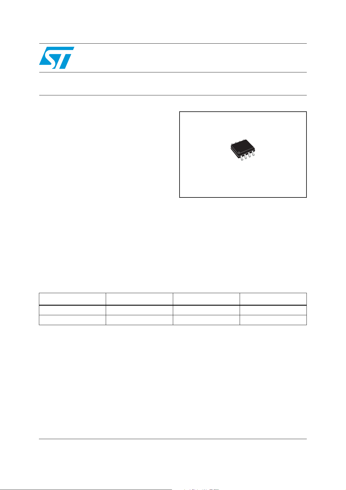
■ SO-8 package
Table 1. Device summary
CC
L9856
High voltage high-side driver
SO-8
Description
The L9856 is an high voltage device,
manufactured with the BCD "OFF-LINE"
technology.
It has the capability of driving N-Channel Power
MOS transistors. The upper (floating) section is
enabled to work with voltage rail up to 160 V. The
logic Inputs are CMOS/TTL compatible for ease
of interfacing with controlling devices.
Order code Operating temp range, °CPackage Packing
L9856 -40 to +125 SO-8 Tube
L9856TR -40 to +125 SO-8 Tape and Reel
May 2008 Rev 2 1/14
www.st.com
1

Contents L9856
Contents
1 Block diagram andpin description . . . . . . . . . . . . . . . . . . . . . . . . . . . . . . . . 5
1.1 Block diagram . . . . . . . . . . . . . . . . . . . . . . . . . . . . . . . . . . . . . . . . . . . . . . . . . 5
1.2 Pin description . . . . . . . . . . . . . . . . . . . . . . . . . . . . . . . . . . . . . . . . . . . . . . . . 5
2 Electrical specifications . . . . . . . . . . . . . . . . . . . . . . . . . . . . . . . . . . . . . . . . 6
2.1 Thermal data . . . . . . . . . . . . . . . . . . . . . . . . . . . . . . . . . . . . . . . . . . . . . . . . . . 6
2.2 Absolute maximum ratings . . . . . . . . . . . . . . . . . . . . . . . . . . . . . . . . . . . . . . . 6
2.3 Recommended operating conditions . . . . . . . . . . . . . . . . . . . . . . . . . . . . . . . 7
2.4 Electrical characteristics . . . . . . . . . . . . . . . . . . . . . . . . . . . . . . . . . . . . . . . . . 7
2.5 Logic table . . . . . . . . . . . . . . . . . . . . . . . . . . . . . . . . . . . . . . . . . . . . . . . . . . . 10
3 Timing diagrams . . . . . . . . . . . . . . . . . . . . . . . . . . . . . . . . . . . . . . . . . . . . . 11
4 Package information . . . . . . . . . . . . . . . . . . . . . . . . . . . . . . . . . . . . . . . . . . 12
5 Revision history . . . . . . . . . . . . . . . . . . . . . . . . . . . . . . . . . . . . . . . . . . . . . . 13
2/14

L9856 List of tables
List of tables
Table 1. Device summary . . . . . . . . . . . . . . . . . . . . . . . . . . . . . . . . . . . . . . . . . . . . . . . . . . . . . . . . . . 1
Table 2. Pin function . . . . . . . . . . . . . . . . . . . . . . . . . . . . . . . . . . . . . . . . . . . . . . . . . . . . . . . . . . . . . . 5
Table 3. Thermal data. . . . . . . . . . . . . . . . . . . . . . . . . . . . . . . . . . . . . . . . . . . . . . . . . . . . . . . . . . . . . 6
Table 4. Absolute maximum ratings . . . . . . . . . . . . . . . . . . . . . . . . . . . . . . . . . . . . . . . . . . . . . . . . . . 6
Table 5. Recommended operating conditions . . . . . . . . . . . . . . . . . . . . . . . . . . . . . . . . . . . . . . . . . . 7
Table 6. Electrical characteristics . . . . . . . . . . . . . . . . . . . . . . . . . . . . . . . . . . . . . . . . . . . . . . . . . . . . 7
Table 7. Logic table . . . . . . . . . . . . . . . . . . . . . . . . . . . . . . . . . . . . . . . . . . . . . . . . . . . . . . . . . . . . . 10
Table 8. Document revision history . . . . . . . . . . . . . . . . . . . . . . . . . . . . . . . . . . . . . . . . . . . . . . . . . 13
3/14

List of figures L9856
List of figures
Figure 1. Block diagram . . . . . . . . . . . . . . . . . . . . . . . . . . . . . . . . . . . . . . . . . . . . . . . . . . . . . . . . . . . . 5
Figure 2. Pin connection (top view) . . . . . . . . . . . . . . . . . . . . . . . . . . . . . . . . . . . . . . . . . . . . . . . . . . . 5
Figure 3. Input/output timing diagram . . . . . . . . . . . . . . . . . . . . . . . . . . . . . . . . . . . . . . . . . . . . . . . . 11
Figure 4. Reset timing diagram . . . . . . . . . . . . . . . . . . . . . . . . . . . . . . . . . . . . . . . . . . . . . . . . . . . . . 11
Figure 5. SO-8 mechanical data and package dimensions . . . . . . . . . . . . . . . . . . . . . . . . . . . . . . . . 12
4/14
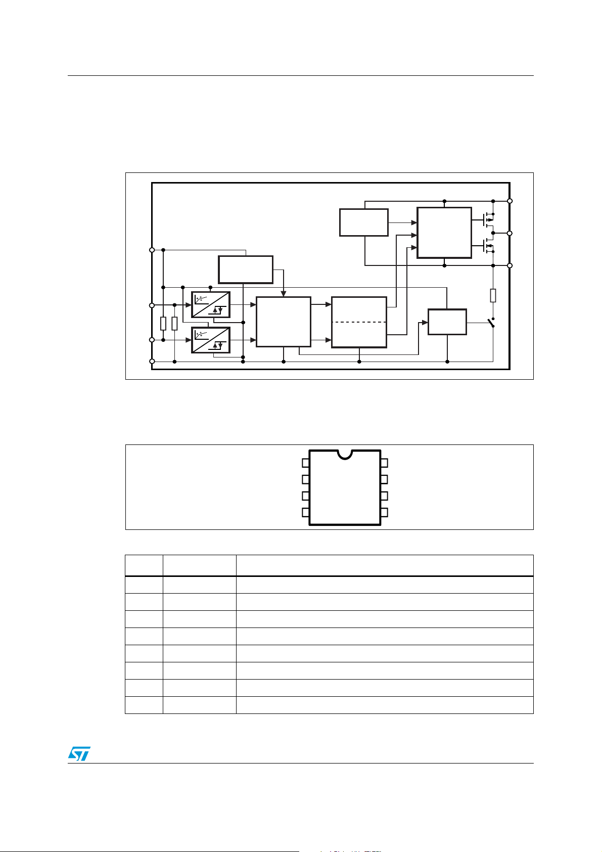
L9856 Block diagram andpin description
1 Block diagram andpin description
1.1 Block diagram
Figure 1. Block diagram
V
B
Undervoltage
RESET
VB to VS
V
CC
Undervoltage
RESET VCC
to GND
Pulse Filter
FLIP FLOP
Break before
Make
H
V
S
O
RES-
IN-
GND
1.2 Pin description
Figure 2. Pin connection (top view)
Table 2. Pin function
Pin # Pin name Description
1V
2 IN- Driver control signal input (negative logic)
3 GND Ground
4 RESET- Driver enable signal input (negative logic)
CC
Logic
Pulse Filter
V
IN-
GND
RESET-
1
CC
2
3
4V
Driver supply, typical 5V
Level Shifter
"ON"
Level Shifter
"OFF"
8
7
6
5
V
B
H
O
NC
S
Delay
Recharge path
5VSMOSFET source connection
6 NC No connection (no bondwire)
7H
8V
O
B
MOSFET gate connection
Driver output stage supply
5/14

Electrical specifications L9856
2 Electrical specifications
2.1 Thermal data
Table 3. Thermal data
Symbol Parameter Value Unit
R
Thermal resistance junction to ambient Max. 150 °C/W
th(j-amb)
2.2 Absolute maximum ratings
Absolute maximum ratings indicate sustained limits beyond which damage to the device may
occur. All voltage parameters are absolute voltages referenced to GND, all currents are defined
positive into any lead. An operation above the absolute maximum limit is not implied and can
damage the part.
Table 4. Absolute maximum ratings
Symbol Parameter
V
BS
V
V
V
HO
V
CC
V
I
IN
V
RES
V
esd
V
CDM
dV/dt Allowable offset voltage slew rate. -50 50 V/nsec
T
T
stg
T
High side floating supply voltage. -0.3 20 V
High side driver output stage voltage
B
transient: 0.5 ms, external MOSFET off.
High side floating supply offset voltage neg.
transient 0.1 µs, repetitive pulse over lifetime at
S
every switching event.
Output voltage gate connection. VS - 0.3 VB + 0.3 V
Supply voltage. -0.3 20 V
Input voltage. -0.3 VCC + 0.3 V
IN
Input injection current. Full function, no latchup; (guaranteed by design). Test at 5 V and 7 V
on Eng. Samples.
Reset input voltage. -0.3 VCC + 0.3 V
Electrostatic discharge voltage (human body
model).
Charge device model CDM, EOS/ESD Ass.
Std 5.3. Number of discharges per pin: 6.
Junction temperature. -55 150
J
Storage temperature. -55 150
Lead temperature (Soldering, 10 seconds) 3
times Bosch soldering profile acc. to Bosch
L
soldering conditions, Gen. Spec.
neg.
Val ue
Units
Min. Max.
-5 166 V
-8 150 V
--- +1 mA
2k V
500 V
°C
- 300
6/14

L9856 Electrical specifications
2.3 Recommended operating conditions
For proper operations the device should be used within the recommended conditions.
(1)
B
S
HO
CC
IN
RES
Val ue
Units
Min. Max.
High side driver output stage voltage VS+4.4 VS+18 V
High side floating supply offset voltage
(25°C)
(125°C)
-3.2
-2.9
150
150
V
Output voltage gate connection VS VBV
Supply voltage 4.4 6.5 V
Input voltage 0 V
Reset input voltage 0 V
(2)
Allowable offset voltage slew rate -50 50 V/nsec
S
Switching frequency 200 kHz
CC
CC
V
V
Table 5. Recommended operating conditions
Symbol Parameter
V
V
V
V
V
V
dV/dt
F
1. Reset-Logic functional for VBS > 2V, independent from VCC-level.
2. Guaranteed by design.
2.4 Electrical characteristics
Table 6. Electrical characteristics
Symbol Parameter Test condition Min. Typ. Max. Unit
V
supply
CC
V
CCUV+
V
CCUV-
V
CCUVHYS
td
UVCC
I
QCC
Unless otherwise specified, V
= 5 V, VBS = 7 V, VS = 0 V, IN = 0 V, RES = 5 V,
CC
load R = 50 Ω, C = 2.5 nF. Unless otherwise noted, these specifications apply for an
operating ambient temperature range of -40 °C < T
VCC supply undervoltage
positive going threshold
VCC supply undervoltage
negative going threshold
VCC supply undervoltage lockout
hysteresis
Undervoltage lockout response
time
VCC supply current 400 µA
rising from 0 V 4.3
V
CC
dropping from 5 V 2.8
V
CC
steps either from 6.5 V
V
CC
to 2.7 V or from 2.7 V to
6.5 V
amb
< 125 °C.
0.02 0.3 0.6
0.5 20 μs
V
7/14

Electrical specifications L9856
Table 6. Electrical characteristics (continued)
Unless otherwise specified, V
= 5 V, VBS = 7 V, VS = 0 V, IN = 0 V, RES = 5 V,
CC
load R = 50 Ω, C = 2.5 nF. Unless otherwise noted, these specifications apply for an
operating ambient temperature range of -40 °C < T
Symbol Parameter Test condition Min. Typ. Max. Unit
VBS supply
amb
< 125 °C.
V
BSUV+
V
BSUV-
V
BSUVHYS
td
UVBS
I
QBS1
VBS supply undervoltage positive
going threshold
VBS supply undervoltage negative
going threshold
VBS supply undervoltage lockout
hysteresis
Undervoltage lockout response
time
VBS supply current
I
QBS2
ΔV
VBS drop due to output turn-on
BS
Gate driver characteristics
I
PKSo1
I
PKSo2
I
PKSo3
I
PKSo4
I
HO,off
t
t
t
t
I
PKSi1
I
PKSi2
Peak output source current
HO off state leakage current guaranteed by design 1 µA
r1
r2
Output rise time
r3
r4
Peak output sink current
I
PKSi3
I
PKSi4
t
f1
t
f2
Output fall time
t
f3
rising from 0 V 4.3 V
V
CC
dropping from 5 V 2.8
V
CC
0.02 0.3 0.4
VBS
steps either from 6.5 V
to 2.7 V or from 2.7 V to 6.5V
static mode,
IN = 0 V or 5 V
static mode, VBS = 16 V,
IN = 0 V or 5 V
C
= 1 µF,
BS
= 3μs, t
td
IG-IN
= 25 °C 120 250
T
j
TEST
= 100μs
0.5 20 µs
100 µA
200 µA
210 mV
70 150
VBS = 16V , Tj = 25 °C 250 500
VBS = 16 V 150 300
= 25 °C 0.2 0.4
T
j
0.3 0.5
VBS = 16 V, Tj = 25 °C 0.1 0.2
VBS = 16 V 0.15 0.3
IN = 5 V, T
= 25 °C 120 250
j
IN = 5 V 70 150
IN = 5 V, Tj = 25 °C
= 16 V
V
BS
250 500
IN = 5 V, VBS = 16 V 150 300
IN = 5 V, T
= 25 °C 0.2 0.4
j
IN = 5 V, 0.3 0.5
VBS = 16 V, IN = 5 V,
Tj = 25 °C
0.1 0.2
V
mA
μs
mA
µs
t
f4
VBS = 16 V, IN = 5 V, 0.15 0.3
8/14

L9856 Electrical specifications
Table 6. Electrical characteristics (continued)
Unless otherwise specified, V
= 5 V, VBS = 7 V, VS = 0 V, IN = 0 V, RES = 5 V,
CC
load R = 50 Ω, C = 2.5 nF. Unless otherwise noted, these specifications apply for an
operating ambient temperature range of -40 °C < T
Symbol Parameter Test condition Min. Typ. Max. Unit
Input-to-output turn-on
t
plhi
t
phli
t
plhr
t
phlr
Input characteristics
propagation delay (50 % input
level to 10 % output level)
Input-to-output turn-off
propagation delay (50 % input
level to 90 % output level)
RES-to-output turn-on
propagation delay (50 % input
level to 10% output level)
RES-to-output turn-off
propagation delay (50 % input
level to 90 % output level)
amb
< 125 °C.
0.1 0.35
0.1 0.4
µs
0.1 0.4
0.1 0.4
V
V
R
V
RESH
V
RESL
R
I
RES
INH
INL
I
IN
RES
High logic level input threshold
Low logic level input threshold
High logic level input resistance 60 100 250 kΩ
IN
High logic level input current VIN = V
High logic level RES input
threshold
Low logic level RES input
threshold
High logic level RES Input
resistance
Low logic level input current V
Recharge characteristics
t
on_rech
t
off_rech
V
RECH
Recharge transistor turn-on
propagation delay
Recharge transistor turn-off
propagation delay
Recharge output transistor onstate voltage drop
Deadtime characteristics
0.6 V
CC
V
= 5V
CC
CC
0.6 V
CC
= 5V
V
CC
0.28
V
CC
5µA
0.28
V
CC
60 100 250 kΩ
= 0 5 µA
RES
V
= 5V 3 6 9 µs
S
0.1 0.5 µs
1 mA forced on recharge
path on
0.5 1.2 V
V
DT
DT
HOFF
HON
High side turn-off to recharge gate
turn-on
Recharge gate turn-off to high
side turn-on
369
= 5 V
V
CC
µs
0.1 0.4 0.7
9/14

Electrical specifications L9856
2.5 Logic table
Table 7. Logic table
Supply voltages
and thresholds
< V
V
cc
CCUV-
V
BS
XX XOFFON
RESET- IN-
XXLOWXOFF ON
X X X HIGH OFF ON
> V
> V
CCUV+
CCUV+
> V
< VB
BSUV+
SUV-
Note: X means independent from signal.
Signals
Output
Ho
Recharge
path
HIGH LOW ON OFF
HIGH LOW OFF OFF
10/14

L9856 Timing diagrams
3 Timing diagrams
Figure 3. Input/output timing diagram
IN
IN
RES
RES
90%
t
t
90%
fx
fx
10%
10%
Vs
Vs
HO
HO
t
t
plhi
plhi
DT
DT
HON
HON
OFF ON
Recharge
Recharge
t
t
OFF ON
off-rech
off-rech
Figure 4. Reset timing diagram
90%
90%
10%
10%
t
t
t
t
phli
phli
DT
DT
HOFF
HOFF
t
t
on-rech
on-rech
rx
rx
IN
IN
RES
RES
HO
HO
t
t
plhr
plhr
t
t
phlr
phlr
11/14

Package information L9856
4 Package information
In order to meet environmental requirements, ST (also) offers these devices in ECOPACK®
packages. ECOPACK
®
packages are lead-free. The category of second Level Interconnect
is marked on the package and on the inner box label, in compliance with JEDEC Standard
JESD97. The maximum ratings related to soldering conditions are also marked on the inner
box label.
ECOPACK is an ST trademark. ECOPACK specifications are available at: www.st.com.
Figure 5. SO-8 mechanical data and package dimensions
DIM.
A 1.750 0.0689
A1 0.100 0.250 0.0039 0.0098
A2 1.250 0.0492
b 0.280 0.480 0.0110 0.0189
c 0.170 0.230 0.0067 0.0091
(1)
D
E 5.800 6.000 6.200 0.2283 0.2362 0.2441
(2)
E1
e 1.270 0.0500
h 0.250 0.500 0.0098 0.0197
L 0.400 1.270 0.0157 0.0500
L1 1.040 0.0409
k0˚8˚0˚8˚
ccc 0.100 0.0039
Notes: 1. Dimensions D does not include mold flash,
2. Dimension “E1” does not include interlead flash
mm inch
MIN. TYP. MAX. MIN. TYP. MAX.
4.800 4.900 5.000 0.1890 0.1929 0.1969
3.800 3.900 4.000 0.1496 0.1535 0.1575
protrusions or gate burrs.
Mold flash, potr usions or gate b urrs shall not
exceed 0.15mm in total (bot h side).
or protrusions. Interlead flash or protrusions shall
not exceed 0.25m m per side.
OUTLINE AND
MECHANICAL DATA
SO-8
12/14
0016023 D

L9856 Revision history
5 Revision history
Table 8. Document revision history
Date Revision Changes
29-Jun-2007 1 Initial release.
Update Features section on page 1.
30-May-2008 2
Updated Table 4: Absolute maximum ratings on page 6.
Updated Table 5: Recommended operating conditions on page 7.
13/14

L9856
Please Read Carefully:
Information in this document is provided solely in connection with ST products. STMicroelectronics NV and its subsidiaries (“ST”) reserve the
right to make changes, corrections, modifications or improvements, to this document, and the products and services described herein at any
time, without notice.
All ST products are sold pursuant to ST’s terms and conditions of sale.
Purchasers are solely responsible for the choice, selection and use of the ST products and services described herein, and ST assumes no
liability whatsoever relating to the choice, selection or use of the ST products and services described herein.
No license, express or implied, by estoppel or otherwise, to any intellectual property rights is granted under this document. If any part of this
document refers to any third party products or services it shall not be deemed a license grant by ST for the use of such third party products
or services, or any intellectual property contained therein or considered as a warranty covering the use in any manner whatsoever of such
third party products or services or any intellectual property contained therein.
UNLESS OTHERWISE SET FORTH IN ST’S TERMS AND CONDITIONS OF SALE ST DISCLAIMS ANY EXPRESS OR IMPLIED
WARRANTY WITH RESPECT TO THE USE AND/OR SALE OF ST PRODUCTS INCLUDING WITHOUT LIMITATION IMPLIED
WARRANTIES OF MERCHANTABILITY, FITNESS FOR A PARTICULAR PURPOSE (AND THEIR EQUIVALENTS UNDER THE LAWS
OF ANY JURISDICTION), OR INFRINGEMENT OF ANY PATENT, COPYRIGHT OR OTHER INTELLECTUAL PROPERTY RIGHT.
UNLESS EXPRESSLY APPROVED IN WRITING BY AN AUTHORIZED ST REPRESENTATIVE, ST PRODUCTS ARE NOT
RECOMMENDED, AUTHORIZED OR WARRANTED FOR USE IN MILITARY, AIR CRAFT, SPACE, LIFE SAVING, OR LIFE SUSTAINING
APPLICATIONS, NOR IN PRODUCTS OR SYSTEMS WHERE FAILURE OR MALFUNCTION MAY RESULT IN PERSONAL INJURY,
DEATH, OR SEVERE PROPERTY OR ENVIRONMENTAL DAMAGE. ST PRODUCTS WHICH ARE NOT SPECIFIED AS "AUTOMOTIVE
GRADE" MAY ONLY BE USED IN AUTOMOTIVE APPLICATIONS AT USER’S OWN RISK.
Resale of ST products with provisions different from the statements and/or technical features set forth in this document shall immediately void
any warranty granted by ST for the ST product or service described herein and shall not create or extend in any manner whatsoever, any
liability of ST.
ST and the ST logo are trademarks or registered trademarks of ST in various countries.
Information in this document supersedes and replaces all information previously supplied.
The ST logo is a registered trademark of STMicroelectronics. All other names are the property of their respective owners.
© 2008 STMicroelectronics - All rights reserved
STMicroelectronics group of companies
Australia - Belgium - Brazil - Canada - China - Czech Republic - Finland - France - Germany - Hong Kong - India - Israel - Italy - Japan -
Malaysia - Malta - Morocco - Singapore - Spain - Sweden - Switzerland - United Kingdom - United States of America
www.st.com
14/14
 Loading...