

L9805E
Super smart power motor driver with 8-Bit MCU,
RAM, EEPROM, ADC, WDG, Timers, PWM and H-bridge driver
Features
■ 6.4-18V Supply Operating Range
■ 16 MHz Maximum Oscillator Frequency
■ 8 MHz Maximum Internal Clock Frequency
■ Oscillator Supervisor
■ Fully Static operation
■ -40°C to + 150°C Temperature Range
■ User EPROM/OTP: 16 Kbytes
■ Data RAM: 256 bytes
■ Data EEPROM: 128 bytes
■ 64 pin HiQUAD64 package
■ 10 multifunctional bidirectional I/O lines
■ Two 16-bit Timers, each featuring:
– 2 Input Captures
– 2 Output Compares
– External Clock input (on Timer 1)
– PWM and Pulse Generator modes
■ Two Programmable 16-bit PWM generator
modules.
■ CAN peripheral including Bus line interface
according 2A/B passive specifications
■ 10-bit Analog-to-Digital Converter
■ Software Watchdog for system integrity
■ Master Reset, Power-On Reset, Low Voltage
Reset
■ 90mΩ DMOS H-bridge.
■ 8-bit Data Manipulation
■ 63 basic Instructions and 17 main Addressing
Modes
■ 8 x 8 Unsigned Multiply Instruction
■ True Bit Manipulation
■ Complete Development Support on
DOS/WINDOWS
■ Full Software Package on DOS/WINDOWS™
(C-Compiler, Cross-Assembler, Debugger).
HiQUAD64
TM
Real-Time Emulator
Order codes
Part number Package Packing
L9805E HiQUAD64 Tray
June 2006 Rev 2 1/127
www.st.com
1

Contents L9805E
Contents
1 General description . . . . . . . . . . . . . . . . . . . . . . . . . . . . . . . . . . . . . . . . . . 9
1.1 Introduction . . . . . . . . . . . . . . . . . . . . . . . . . . . . . . . . . . . . . . . . . . . . . . . . 9
1.2 OTP, ROM and EPROM devices . . . . . . . . . . . . . . . . . . . . . . . . . . . . . . . . 9
1.3 Pin out . . . . . . . . . . . . . . . . . . . . . . . . . . . . . . . . . . . . . . . . . . . . . . . . . . . 11
1.4 Pin Description . . . . . . . . . . . . . . . . . . . . . . . . . . . . . . . . . . . . . . . . . . . . . 11
1.5 Register & Memory Map . . . . . . . . . . . . . . . . . . . . . . . . . . . . . . . . . . . . . 12
2 Central Processing Unit . . . . . . . . . . . . . . . . . . . . . . . . . . . . . . . . . . . . . 16
2.1 Introduction . . . . . . . . . . . . . . . . . . . . . . . . . . . . . . . . . . . . . . . . . . . . . . . 16
2.2 CPU registers . . . . . . . . . . . . . . . . . . . . . . . . . . . . . . . . . . . . . . . . . . . . . . 16
3 Clocks, Reset, Interrupts & Power saving modes . . . . . . . . . . . . . . . . 19
3.1 Clock system . . . . . . . . . . . . . . . . . . . . . . . . . . . . . . . . . . . . . . . . . . . . . . 19
3.1.1 General Description . . . . . . . . . . . . . . . . . . . . . . . . . . . . . . . . . . . . . . . . 19
3.1.2 External Clock . . . . . . . . . . . . . . . . . . . . . . . . . . . . . . . . . . . . . . . . . . . . 20
3.2 Oscillator safeguard . . . . . . . . . . . . . . . . . . . . . . . . . . . . . . . . . . . . . . . . . 21
3.2.1 Dedicated Control Status Register . . . . . . . . . . . . . . . . . . . . . . . . . . . . 21
3.3 Watchdog system (WDG) . . . . . . . . . . . . . . . . . . . . . . . . . . . . . . . . . . . . . 22
3.3.1 Introduction . . . . . . . . . . . . . . . . . . . . . . . . . . . . . . . . . . . . . . . . . . . . . . 22
3.3.2 Main Features . . . . . . . . . . . . . . . . . . . . . . . . . . . . . . . . . . . . . . . . . . . . 22
3.3.3 Functional Description . . . . . . . . . . . . . . . . . . . . . . . . . . . . . . . . . . . . . . 22
3.3.4 Register Description . . . . . . . . . . . . . . . . . . . . . . . . . . . . . . . . . . . . . . . 24
3.4 Miscellaneous Register . . . . . . . . . . . . . . . . . . . . . . . . . . . . . . . . . . . . . . 24
3.5 Reset . . . . . . . . . . . . . . . . . . . . . . . . . . . . . . . . . . . . . . . . . . . . . . . . . . . . 25
3.5.1 Introduction . . . . . . . . . . . . . . . . . . . . . . . . . . . . . . . . . . . . . . . . . . . . . . 25
3.5.2 External Reset . . . . . . . . . . . . . . . . . . . . . . . . . . . . . . . . . . . . . . . . . . . . 26
3.5.3 Reset Operation . . . . . . . . . . . . . . . . . . . . . . . . . . . . . . . . . . . . . . . . . . . 26
3.5.4 Power-on Reset - Low Voltage Detection . . . . . . . . . . . . . . . . . . . . . . . 26
3.6 Interrupts . . . . . . . . . . . . . . . . . . . . . . . . . . . . . . . . . . . . . . . . . . . . . . . . . 28
3.7 Power Saving Modes . . . . . . . . . . . . . . . . . . . . . . . . . . . . . . . . . . . . . . . . 30
3.7.1 Introduction . . . . . . . . . . . . . . . . . . . . . . . . . . . . . . . . . . . . . . . . . . . . . . 30
3.7.2 Slow Mode . . . . . . . . . . . . . . . . . . . . . . . . . . . . . . . . . . . . . . . . . . . . . . . 30
3.7.3 Wait Mode . . . . . . . . . . . . . . . . . . . . . . . . . . . . . . . . . . . . . . . . . . . . . . . 30
2/127

L9805E Contents
3.7.4 Halt Mode . . . . . . . . . . . . . . . . . . . . . . . . . . . . . . . . . . . . . . . . . . . . . . . 31
4 Voltage Regulator . . . . . . . . . . . . . . . . . . . . . . . . . . . . . . . . . . . . . . . . . . 32
4.1 Introduction . . . . . . . . . . . . . . . . . . . . . . . . . . . . . . . . . . . . . . . . . . . . . . . 32
4.1.1 Functional Description . . . . . . . . . . . . . . . . . . . . . . . . . . . . . . . . . . . . . . 32
4.2 Digital Section Power Supply . . . . . . . . . . . . . . . . . . . . . . . . . . . . . . . . . . 33
4.2.1 VDD Short Circuit Protection . . . . . . . . . . . . . . . . . . . . . . . . . . . . . . . . . 33
4.3 Analog Section Power Supply . . . . . . . . . . . . . . . . . . . . . . . . . . . . . . . . . 33
4.3.1 VCC Short Circuit Protection . . . . . . . . . . . . . . . . . . . . . . . . . . . . . . . . . 33
5 On-Chip Peripherals . . . . . . . . . . . . . . . . . . . . . . . . . . . . . . . . . . . . . . . . 34
5.1 I/O Ports . . . . . . . . . . . . . . . . . . . . . . . . . . . . . . . . . . . . . . . . . . . . . . . . . . 34
5.1.1 Introduction . . . . . . . . . . . . . . . . . . . . . . . . . . . . . . . . . . . . . . . . . . . . . . 34
5.1.2 Functional Description . . . . . . . . . . . . . . . . . . . . . . . . . . . . . . . . . . . . . . 34
5.1.3 Register Description . . . . . . . . . . . . . . . . . . . . . . . . . . . . . . . . . . . . . . . 41
5.2 16-Bit Timer . . . . . . . . . . . . . . . . . . . . . . . . . . . . . . . . . . . . . . . . . . . . . . . 42
5.2.1 Introduction . . . . . . . . . . . . . . . . . . . . . . . . . . . . . . . . . . . . . . . . . . . . . . 42
5.2.2 Main Features . . . . . . . . . . . . . . . . . . . . . . . . . . . . . . . . . . . . . . . . . . . . 43
5.2.3 Functional Description . . . . . . . . . . . . . . . . . . . . . . . . . . . . . . . . . . . . . . 43
5.2.4 Register Description . . . . . . . . . . . . . . . . . . . . . . . . . . . . . . . . . . . . . . . 54
5.3 PWM Generator . . . . . . . . . . . . . . . . . . . . . . . . . . . . . . . . . . . . . . . . . . . . 62
5.3.1 Introduction . . . . . . . . . . . . . . . . . . . . . . . . . . . . . . . . . . . . . . . . . . . . . . 62
5.3.2 Functional Description . . . . . . . . . . . . . . . . . . . . . . . . . . . . . . . . . . . . . . 63
5.3.3 Register Description . . . . . . . . . . . . . . . . . . . . . . . . . . . . . . . . . . . . . . . 64
5.4 PWM I/O . . . . . . . . . . . . . . . . . . . . . . . . . . . . . . . . . . . . . . . . . . . . . . . . . . 68
5.4.1 Introduction . . . . . . . . . . . . . . . . . . . . . . . . . . . . . . . . . . . . . . . . . . . . . . 68
5.4.2 PWMO . . . . . . . . . . . . . . . . . . . . . . . . . . . . . . . . . . . . . . . . . . . . . . . . . . 68
5.4.3 PWMI . . . . . . . . . . . . . . . . . . . . . . . . . . . . . . . . . . . . . . . . . . . . . . . . . . . 69
5.5 10-BIT A/D Converter (AD10) . . . . . . . . . . . . . . . . . . . . . . . . . . . . . . . . . 70
5.5.1 Introduction . . . . . . . . . . . . . . . . . . . . . . . . . . . . . . . . . . . . . . . . . . . . . . 70
5.5.2 Functional Description . . . . . . . . . . . . . . . . . . . . . . . . . . . . . . . . . . . . . . 70
5.5.3 Input Selections and Sampling . . . . . . . . . . . . . . . . . . . . . . . . . . . . . . . 71
5.5.4 Interrupt Management . . . . . . . . . . . . . . . . . . . . . . . . . . . . . . . . . . . . . . 71
5.5.5 Temperature Sensing . . . . . . . . . . . . . . . . . . . . . . . . . . . . . . . . . . . . . . . 71
5.5.6 Precise Temperature Measurement . . . . . . . . . . . . . . . . . . . . . . . . . . . . 72
5.5.7 Register Description . . . . . . . . . . . . . . . . . . . . . . . . . . . . . . . . . . . . . . . 73
3/127

Contents L9805E
5.6 Controller Area Network (CAN) . . . . . . . . . . . . . . . . . . . . . . . . . . . . . . . . 75
5.6.1 Introduction . . . . . . . . . . . . . . . . . . . . . . . . . . . . . . . . . . . . . . . . . . . . . . 75
5.6.2 Main Features . . . . . . . . . . . . . . . . . . . . . . . . . . . . . . . . . . . . . . . . . . . . 76
5.6.3 Functional Description . . . . . . . . . . . . . . . . . . . . . . . . . . . . . . . . . . . . . . 76
5.6.4 Register Description . . . . . . . . . . . . . . . . . . . . . . . . . . . . . . . . . . . . . . . 82
5.7 CAN BUS TRANSCEIVER . . . . . . . . . . . . . . . . . . . . . . . . . . . . . . . . . . . . 93
5.7.1 Introduction . . . . . . . . . . . . . . . . . . . . . . . . . . . . . . . . . . . . . . . . . . . . . . 93
5.7.2 Main Features . . . . . . . . . . . . . . . . . . . . . . . . . . . . . . . . . . . . . . . . . . . . 93
5.7.3 Functional Description . . . . . . . . . . . . . . . . . . . . . . . . . . . . . . . . . . . . . . 94
5.7.4 CAN Transceiver Disabling function . . . . . . . . . . . . . . . . . . . . . . . . . . . . 94
5.8 Power Bridge . . . . . . . . . . . . . . . . . . . . . . . . . . . . . . . . . . . . . . . . . . . . . . 94
5.8.1 Introduction . . . . . . . . . . . . . . . . . . . . . . . . . . . . . . . . . . . . . . . . . . . . . . 94
5.8.2 Main Features . . . . . . . . . . . . . . . . . . . . . . . . . . . . . . . . . . . . . . . . . . . . 95
5.8.3 Functional Description . . . . . . . . . . . . . . . . . . . . . . . . . . . . . . . . . . . . . . 95
5.8.4 Interrupt generation . . . . . . . . . . . . . . . . . . . . . . . . . . . . . . . . . . . . . . . . 97
5.8.5 Operating Modes . . . . . . . . . . . . . . . . . . . . . . . . . . . . . . . . . . . . . . . . . . 97
5.8.6 Register Description . . . . . . . . . . . . . . . . . . . . . . . . . . . . . . . . . . . . . . 100
5.9 EEPROM (EEP) . . . . . . . . . . . . . . . . . . . . . . . . . . . . . . . . . . . . . . . . . . . 101
5.9.1 Introduction . . . . . . . . . . . . . . . . . . . . . . . . . . . . . . . . . . . . . . . . . . . . . 101
5.9.2 Functional description . . . . . . . . . . . . . . . . . . . . . . . . . . . . . . . . . . . . . 102
5.9.3 Register Description . . . . . . . . . . . . . . . . . . . . . . . . . . . . . . . . . . . . . . 104
6 Instruction Set . . . . . . . . . . . . . . . . . . . . . . . . . . . . . . . . . . . . . . . . . . . . 106
6.1 ST7 Addressing Modes . . . . . . . . . . . . . . . . . . . . . . . . . . . . . . . . . . . . . 106
6.2 Instruction groups . . . . . . . . . . . . . . . . . . . . . . . . . . . . . . . . . . . . . . . . . . 112
7 Electrical Characteristics . . . . . . . . . . . . . . . . . . . . . . . . . . . . . . . . . . . 115
7.1 Absolute Maximum Ratings . . . . . . . . . . . . . . . . . . . . . . . . . . . . . . . . . . 115
7.2 Power considerations . . . . . . . . . . . . . . . . . . . . . . . . . . . . . . . . . . . . . . . 116
7.3 Application diagram example . . . . . . . . . . . . . . . . . . . . . . . . . . . . . . . . . 118
7.4 DC Electrical Characteristics . . . . . . . . . . . . . . . . . . . . . . . . . . . . . . . . . 119
7.5 Control Timing . . . . . . . . . . . . . . . . . . . . . . . . . . . . . . . . . . . . . . . . . . . . 120
7.6 Operating block electrical characteristics . . . . . . . . . . . . . . . . . . . . . . . . 121
8 Package information . . . . . . . . . . . . . . . . . . . . . . . . . . . . . . . . . . . . . . . 125
4/127

L9805E Contents
9 Revision history . . . . . . . . . . . . . . . . . . . . . . . . . . . . . . . . . . . . . . . . . . 126
5/127

List of tables L9805E
List of tables
Table 1. Memory Map. . . . . . . . . . . . . . . . . . . . . . . . . . . . . . . . . . . . . . . . . . . . . . . . . . . . . . . . . . . . 13
Table 2. Recommended Values for 16 MHz Crystal Resonator . . . . . . . . . . . . . . . . . . . . . . . . . . . . 19
Table 3. Watchdog Timing (fOSC = 16 MHz) . . . . . . . . . . . . . . . . . . . . . . . . . . . . . . . . . . . . . . . . . . 23
Table 4. Interrupt Mapping . . . . . . . . . . . . . . . . . . . . . . . . . . . . . . . . . . . . . . . . . . . . . . . . . . . . . . . . 28
Table 5. I/O Port Mode Options . . . . . . . . . . . . . . . . . . . . . . . . . . . . . . . . . . . . . . . . . . . . . . . . . . . . 36
Table 6. I/O Port Configurations . . . . . . . . . . . . . . . . . . . . . . . . . . . . . . . . . . . . . . . . . . . . . . . . . . . . 37
Table 7. Port A Configuration . . . . . . . . . . . . . . . . . . . . . . . . . . . . . . . . . . . . . . . . . . . . . . . . . . . . . . 39
Table 8. Port B Configuration . . . . . . . . . . . . . . . . . . . . . . . . . . . . . . . . . . . . . . . . . . . . . . . . . . . . . . 39
Table 9. Clock Control Bits . . . . . . . . . . . . . . . . . . . . . . . . . . . . . . . . . . . . . . . . . . . . . . . . . . . . . . . . 56
Table 10. 16-Bit Timer Register Map and Reset Values . . . . . . . . . . . . . . . . . . . . . . . . . . . . . . . . . . 61
Table 11. PWM Timing (fCPU = 8MHz) . . . . . . . . . . . . . . . . . . . . . . . . . . . . . . . . . . . . . . . . . . . . . . . 67
Table 12. ADC Channel Selection Table . . . . . . . . . . . . . . . . . . . . . . . . . . . . . . . . . . . . . . . . . . . . . . 74
Table 13. CAN Register Map and Reset Values . . . . . . . . . . . . . . . . . . . . . . . . . . . . . . . . . . . . . . . . 92
Table 14. Functional Description Table . . . . . . . . . . . . . . . . . . . . . . . . . . . . . . . . . . . . . . . . . . . . . . . 98
Table 15. ST7 Addressing Mode Overview: . . . . . . . . . . . . . . . . . . . . . . . . . . . . . . . . . . . . . . . . . . . 106
Table 16. Absolute Maximum Ratings (Voltage Referenced to GND) . . . . . . . . . . . . . . . . . . . . . . . 115
Table 17. Thermal Characteristics (VB=18V, TJ = 150°C, ILOAD = 2A) . . . . . . . . . . . . . . . . . . . . . 116
Table 18. DC Electrical Characteristics . . . . . . . . . . . . . . . . . . . . . . . . . . . . . . . . . . . . . . . . . . . . . . 119
Table 19. Control Timing . . . . . . . . . . . . . . . . . . . . . . . . . . . . . . . . . . . . . . . . . . . . . . . . . . . . . . . . . 120
Table 20. A/D converter . . . . . . . . . . . . . . . . . . . . . . . . . . . . . . . . . . . . . . . . . . . . . . . . . . . . . . . . . . 121
Table 21. POWER Bridge. . . . . . . . . . . . . . . . . . . . . . . . . . . . . . . . . . . . . . . . . . . . . . . . . . . . . . . . . 121
Table 22. EEPROM . . . . . . . . . . . . . . . . . . . . . . . . . . . . . . . . . . . . . . . . . . . . . . . . . . . . . . . . . . . . . 122
Table 23. PWM OUTPUT . . . . . . . . . . . . . . . . . . . . . . . . . . . . . . . . . . . . . . . . . . . . . . . . . . . . . . . . . 122
Table 24. PWM INPUT . . . . . . . . . . . . . . . . . . . . . . . . . . . . . . . . . . . . . . . . . . . . . . . . . . . . . . . . . . . 122
Table 25. Oscillator Safeguard . . . . . . . . . . . . . . . . . . . . . . . . . . . . . . . . . . . . . . . . . . . . . . . . . . . . . 122
Table 26. CAN Transceiver . . . . . . . . . . . . . . . . . . . . . . . . . . . . . . . . . . . . . . . . . . . . . . . . . . . . . . . 123
Table 27. Power on/low voltage reset. . . . . . . . . . . . . . . . . . . . . . . . . . . . . . . . . . . . . . . . . . . . . . . . 124
Table 28. Document revision history . . . . . . . . . . . . . . . . . . . . . . . . . . . . . . . . . . . . . . . . . . . . . . . . 126
6/127

L9805E List of figures
List of figures
Figure 1. L9805E Block Diagram . . . . . . . . . . . . . . . . . . . . . . . . . . . . . . . . . . . . . . . . . . . . . . . . . . . . 10
Figure 2. Pin out. . . . . . . . . . . . . . . . . . . . . . . . . . . . . . . . . . . . . . . . . . . . . . . . . . . . . . . . . . . . . . . . . 11
Figure 3. Organization of Internal CPU Registers . . . . . . . . . . . . . . . . . . . . . . . . . . . . . . . . . . . . . . . 16
Figure 4. Stack Manipulation on Interrupt . . . . . . . . . . . . . . . . . . . . . . . . . . . . . . . . . . . . . . . . . . . . . 18
Figure 5. External Clock Source Connections . . . . . . . . . . . . . . . . . . . . . . . . . . . . . . . . . . . . . . . . . . 19
Figure 6. Crystal/Ceramic Resonator. . . . . . . . . . . . . . . . . . . . . . . . . . . . . . . . . . . . . . . . . . . . . . . . . 20
Figure 7. Clock Prescaler Block Diagram . . . . . . . . . . . . . . . . . . . . . . . . . . . . . . . . . . . . . . . . . . . . . 20
Figure 8. Timing Diagram for Internal CPU Clock Frequency transitions . . . . . . . . . . . . . . . . . . . . . 21
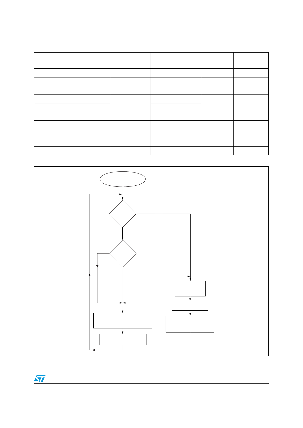
Figure 9. Functional Description . . . . . . . . . . . . . . . . . . . . . . . . . . . . . . . . . . . . . . . . . . . . . . . . . . . . 23
Figure 10. Power Up/Down behaviour . . . . . . . . . . . . . . . . . . . . . . . . . . . . . . . . . . . . . . . . . . . . . . . . . 27
Figure 11. Reset Block Diagram . . . . . . . . . . . . . . . . . . . . . . . . . . . . . . . . . . . . . . . . . . . . . . . . . . . . . 27
Figure 12. Interrupt Processing Flowchart . . . . . . . . . . . . . . . . . . . . . . . . . . . . . . . . . . . . . . . . . . . . . . 29
Figure 13. Wait Mode Flow Chart . . . . . . . . . . . . . . . . . . . . . . . . . . . . . . . . . . . . . . . . . . . . . . . . . . . . 30
Figure 14. Halt Mode Flow Chart . . . . . . . . . . . . . . . . . . . . . . . . . . . . . . . . . . . . . . . . . . . . . . . . . . . . . 31
Figure 15. Voltage regulation block diagram . . . . . . . . . . . . . . . . . . . . . . . . . . . . . . . . . . . . . . . . . . . . 32
Figure 16. I/O Port General Block Diagram . . . . . . . . . . . . . . . . . . . . . . . . . . . . . . . . . . . . . . . . . . . . . 36
Figure 17. Interrupt I/O Port State Transitions . . . . . . . . . . . . . . . . . . . . . . . . . . . . . . . . . . . . . . . . . . . 38
Figure 18. Ports PA0-PA7, PB0-PB1I . . . . . . . . . . . . . . . . . . . . . . . . . . . . . . . . . . . . . . . . . . . . . . . . . 40
Figure 19. Timer Block Diagram . . . . . . . . . . . . . . . . . . . . . . . . . . . . . . . . . . . . . . . . . . . . . . . . . . . . . 44
Figure 20. Counter Timing Diagram, internal clock divided by 2 . . . . . . . . . . . . . . . . . . . . . . . . . . . . . 46
Figure 21. Counter Timing Diagram, internal clock divided by 4 . . . . . . . . . . . . . . . . . . . . . . . . . . . . . 46
Figure 22. Counter Timing Diagram, internal clock divided by 8 . . . . . . . . . . . . . . . . . . . . . . . . . . . . . 46
Figure 23. Input Capture Block Diagram . . . . . . . . . . . . . . . . . . . . . . . . . . . . . . . . . . . . . . . . . . . . . . . 48
Figure 24. Input Capture Timing Diagram . . . . . . . . . . . . . . . . . . . . . . . . . . . . . . . . . . . . . . . . . . . . . . 48
Figure 25. Output Compare Block Diagram . . . . . . . . . . . . . . . . . . . . . . . . . . . . . . . . . . . . . . . . . . . . . 50
Figure 26. Output Compare Timing Diagram, Internal Clock Divided by 2 . . . . . . . . . . . . . . . . . . . . . 50
Figure 27. One Pulse Mode Timing . . . . . . . . . . . . . . . . . . . . . . . . . . . . . . . . . . . . . . . . . . . . . . . . . . . 52
Figure 28. Pulse Width Modulation Mode Timing . . . . . . . . . . . . . . . . . . . . . . . . . . . . . . . . . . . . . . . . 54
Figure 29. PWM Cycle . . . . . . . . . . . . . . . . . . . . . . . . . . . . . . . . . . . . . . . . . . . . . . . . . . . . . . . . . . . . . 64
Figure 30. PWM Generation . . . . . . . . . . . . . . . . . . . . . . . . . . . . . . . . . . . . . . . . . . . . . . . . . . . . . . . . 64
Figure 31. PWM Block Diagram. . . . . . . . . . . . . . . . . . . . . . . . . . . . . . . . . . . . . . . . . . . . . . . . . . . . . . 67
Figure 32. PWM I/O Block Diagram . . . . . . . . . . . . . . . . . . . . . . . . . . . . . . . . . . . . . . . . . . . . . . . . . . . 68
Figure 33. Impedance at PWMO/I pin . . . . . . . . . . . . . . . . . . . . . . . . . . . . . . . . . . . . . . . . . . . . . . . . . 69
Figure 34. PWMI function . . . . . . . . . . . . . . . . . . . . . . . . . . . . . . . . . . . . . . . . . . . . . . . . . . . . . . . . . . 69
Figure 35. Block diagram of the Analog to Digital Converter . . . . . . . . . . . . . . . . . . . . . . . . . . . . . . . . 71
Figure 36. Temperature Sensor output . . . . . . . . . . . . . . . . . . . . . . . . . . . . . . . . . . . . . . . . . . . . . . . . 72
Figure 37. CAN Block Diagram . . . . . . . . . . . . . . . . . . . . . . . . . . . . . . . . . . . . . . . . . . . . . . . . . . . . . . 75
Figure 38. CAN Frames . . . . . . . . . . . . . . . . . . . . . . . . . . . . . . . . . . . . . . . . . . . . . . . . . . . . . . . . . . . . 78
Figure 39. CAN Controller State Diagram . . . . . . . . . . . . . . . . . . . . . . . . . . . . . . . . . . . . . . . . . . . . . . 79
Figure 40. CAN Error State Diagram . . . . . . . . . . . . . . . . . . . . . . . . . . . . . . . . . . . . . . . . . . . . . . . . . . 81
Figure 41. Bit Timing . . . . . . . . . . . . . . . . . . . . . . . . . . . . . . . . . . . . . . . . . . . . . . . . . . . . . . . . . . . . . . 82
Figure 42. CAN Register Map . . . . . . . . . . . . . . . . . . . . . . . . . . . . . . . . . . . . . . . . . . . . . . . . . . . . . . . 91
Figure 43. Page Maps . . . . . . . . . . . . . . . . . . . . . . . . . . . . . . . . . . . . . . . . . . . . . . . . . . . . . . . . . . . . . 92
Figure 44. Can Bus Transceiver Block Diagram . . . . . . . . . . . . . . . . . . . . . . . . . . . . . . . . . . . . . . . . . 94
Figure 45. Power Bridge Schematic . . . . . . . . . . . . . . . . . . . . . . . . . . . . . . . . . . . . . . . . . . . . . . . . . . 96
Figure 46. Example - Power Bridge Waveform, PWM Up Brake Driving Mode. . . . . . . . . . . . . . . . . 100
Figure 47. EEPROM Block Diagram . . . . . . . . . . . . . . . . . . . . . . . . . . . . . . . . . . . . . . . . . . . . . . . . . 102
Figure 48. Data EEPROM Programming Cycle . . . . . . . . . . . . . . . . . . . . . . . . . . . . . . . . . . . . . . . . . 103
7/127

List of figures L9805E
Figure 49. EEPROM Programming Flowchart . . . . . . . . . . . . . . . . . . . . . . . . . . . . . . . . . . . . . . . . . . 103
Figure 50. HiQUAD-64: qJA. . . . . . . . . . . . . . . . . . . . . . . . . . . . . . . . . . . . . . . . . . . . . . . . . . . . . . . . 117
Figure 51. HiQUAD-64: Thermal impedance . . . . . . . . . . . . . . . . . . . . . . . . . . . . . . . . . . . . . . . . . . . 117
Figure 52. Application diagram example . . . . . . . . . . . . . . . . . . . . . . . . . . . . . . . . . . . . . . . . . . . . . . 118
Figure 53. HiQUAD-64 Mechanical Data & Package Dimensions. . . . . . . . . . . . . . . . . . . . . . . . . . . 125
8/127

L9805E General description
1 General description
1.1 Introduction
The L9805E is a Super Smart Power device suited to drive resistive and inductive loads
under software control. It includes a ST7 microcontroller and some pheripherals. The
microcontroller can execute the software contained in the program EPROM/ROM and drive,
through dedicated registers, the power bridge.
The internal voltage regulators rated to the automotive environment, PWM modules, CAN
transceiver and controller, timers, temperature sensor and the AtoD converter allow the
device to realize by itself a complete application, in line with the most common mechatronic
requirements.
1.2 OTP, ROM and EPROM devices
For development purposes the device is available in plastic HiQuad package without window
rating in the OTP class.
Mass production is supported by means of ROM devices.
Engineering samples could be assembled using window packages. These are generally
referenced as “EPROM devices”.
EPROM devices are erased by exposure to high intensity UV light admitted through the
transparent window. This exposure discharges the floating gate to its initial state through
induced photo current.
It is recommended to keep the L9805E device out of direct sunlight, since the UV content of
sunlight can be sufficient to cause functional failure. Extended exposure to room level
fluorescent lighting may also cause erasure.
An opaque coating (paint, tape, label, etc...) should be placed over the package window if
the product is to be operated under these lighting conditions. Covering the window also
reduces I
An Ultraviolet source of wave length 2537 Å yielding a total integrated dosage of 15 Wattsec/cm
such a UV lamp with a 12mW/cm
without any interposed filters.
OTP and EPROM devices can be programmed by a dedicated Eprom Programming Board
and software that are part of the development tool-set.
in power-saving modes due to photo-diode leakage currents.
DD
2
is required to erase the EPROM. The device will be erased in 40 to 45minutes if
2
power rating is placed 1 inch from the device window
9/127
General description L9805E
Figure 1. L9805E Block Diagram
OSCIN
OSCOUT
NRESET
VPP/TM
CAN_H
CAN_L
OSC
OSC SAFEGUARD
CONTROL
8-BIT CORE
ALU
ROM/OTP/EPROM
16K
RAM 256B
EEPROM 128B
WATCHDOG
CAN
CONTROLLER
RX TX
CAN
TRANSCEIVER
Internal
CLOCK
PREREGULATOR
POWER
SUPPLY
POWER
BRIDGE
ADDRESS AND DATA BUS
TEMP SENSOR
10-bit ADC
PWM 1
PWM 2
PWMO
VB1
VB2
V
DD
V
CC
GND
AGND
VBR
VBL
OUTR
OUTL
PGND
AD2
AD3
AD4
PWMO
PWMI
PORT B
TIMER 2
PORT A
TIMER 1
PWMI
PB0 -> PB1
PA0 -> PA7
10/127
L9805E General description
1.3 Pin out
Figure 2. Pin out
VCC
AGND
AD4
PA2/ICAP2_1
PA3/ICAP1_1
PGND
PGND
PA4/EXTCLK_1
PA5/OCMP2_2
PA6/OCMP1_2
PA7/ICAP2_2
PB0/ICAP1_2
NU
NU
NU
AD3
AD2
PA1/OCMP1_1
PA0/OCMP2_1
VPP/TM
VDD
OSCIN
OSCOUT
GND
NU
VBL
VBL
VBL
NU
NU
NU
NU
64 63 62 61 60 59 58 57 56 55 54 53
1
2
3
4
5
6
7
8
9
10
11
12
13
14
15
16
17
18
19
20
21 22 23 24
NU
NU
25 26
OUTL
OUTL
OUTL
PGND
27 28
PGND
29 30 31 32
OUTR
OUTR
NU
52
PB1/EXTCLK_2
51
NU
50
NU
49
PWMO
48
PWMI
47
45
44
43
42
41
40
39
38
37
36
35
34
33
NRESET
CAN_H
CAN_L
GND
VDD
VB2
VB1
VBR
VBR
VBR
NU
NU
NU
NU
46
NU
NU
OUTR
1.4 Pin Description
AD2-AD4: Analog input to ADC.
PA0/OCMP2_1-PA1/OCMP1_1: I/Os or Output compares on Timer 1. Alternate function
software selectable (by setting OC2E or OC1E in CR2 register: bit 6 or 7 at 0031h). When
used as an alternate function, this pin is a push-pull output as requested by Timer 1.
Otherwise, this pin is a triggered floating input or a push-pull output.
PA2/ICAP2_1-PA3/ICAP1_1: I/Os or Input captures on Timer 1. Before using this I/O as
alternate inputs, they must be configured by software in input mode (DDR=0). In this case,
these pins are a triggered floating input. Otherwise (I/O function), these pin are triggered
floating inputs or push-pull outputs.
PA4/EXTCLK_1: PA4 I/O or External Clock on Timer 1. Before using this I/O as alternate
input, it must be configured by software in input mode (DDR=0). In this case, this pin is a
triggered floating input. Otherwise (I/O function), this pin is a triggered floating input or a
push-pull output.
11/127

General description L9805E
PA5/OCMP2_2-PA6/OCMP1_2: I/Os or Output Compares on Timer 2. Alternate function
software selectable (by setting OC2E or OC1E in CR2 register: bit 6 or 7 at 0041h). When
used as alternate functions, these pins are push-pull outputs as requested by Timer 2.
Otherwise, these pins are triggered floating inputs or push-pull outputs.
PA7/ICAP2_2-PB0/ICAP1_2: I/Os or Input Captures on Timer 2. Before using these I/Os as
alternate inputs, they must be configured by software in input mode (DDR=0). In this case,
these pins are triggered floating inputs. Otherwise (I/O function), these pins are triggered
floating inputs or push-pull outputs.
PB1/EXTCLK_2: PB1 I/O or External Clock on Timer 2. Before using this I/O as alternate
input, it must be configured by software in input mode (DDR=0). In this case, this pin is a
triggered floating input. Otherwise (I/O function), this pin is a triggered floating input or a
push-pull output.
VPP/TM: Input. This pin must be held low during normal operating modes.
VDD: Output. 5V Power supply for digital circuits, from internal voltage regulator.
OSCIN: Input Oscillator pin.
OSCOUT: Output Oscillator pin.
GND: Ground for digital circuits.
VBR: Power supply for Right half-bridge.
OUTR: Output of Left half-bridge.
PGND: Ground for power transistor.
OUTL: Output of Right half-bridge.
VBL: Power supply for Left half-bridge.
VB1: Power supply for voltage regulators.
VB2: Pre-regulated voltage for analog circuits.
CAN_L: Low side CAN bus output.
CAN_H: High side CAN bus input.
NRESET: Bidirectional. This active low signal forces the initialization of the MCU. This event
is the top priority non maskable interrupt. It can be used to reset external peripherals.
PWMI: PWM input. Directly connected to Input Capture 2 on Timer 2.
PWMO: PWM output. Connected to the output of PWM2 module.
AGND: Ground for all analog circuitry (except power bridge).
VCC: Output. 5V power supply for analog circuits, from internal voltage regulator.
1.5 Register & Memory Map
As shown in the Ta bl e 1 , the MCU is capable of addressing 64K bytes of memories and I/O
registers. In this MCU, 63742 of these bytes are user accessible.
The available memory locations consist of 128 bytes of I/O registers, 256 bytes of RAM, 128
bytes of EEPROM and 16Kbytes of user EPROM/ROM. The RAM space includes 64bytes
for the stack from 0140h to 017Fh.
12/127
L9805E General description
The highest address bytes contain the user reset and interrupt vectors.
Table 1. Memory Map
Address Block
0000h
0001h
0002h
Port A
0003h
0004h
0005h
0006h
Port B
0007h
0008h to
000Fh
0010h
0011h
0012h
0013h
PWM1
0014h
0015h
0016h
Register
Label
PADR ..
PADDR ..
PAOR ..
PBDR ..
PBDDR ..
PBOR ..
P1CYRH ..
P1CYRL ..
P1DRH ..
P1DRL ..
P1CR ..
P1CTH ..
P1CTL ..
Register name
Data Register
Data Direction Register
Option Register
Not Used
Data Register
Data Direction Register
Option Register
Not Used
RESERVED
PWM1 Cycle Register High
PWM1 Cycle Register Low
PWM1 Duty Register High
PWM1 Duty Register Low
PWM1 Control Register
PWM1 Counter Register High
PWM1 Counter Register Low
0017h RESERVED
0018h
0019h
001Ah
001Bh
001Ch
001Dh
001Eh
PWM2
P2CYRH ..
P2CYRL ..
P2DRH ..
P2DRL ..
P2CR ..
P2CTH ..
P2CTL ..
PWM2 Cycle Register High
PWM2 Cycle Register Low
PWM2 Duty Register High
PWM2 Duty Register Low
PWM2 Control Register
PWM2 Counter Register High
PWM2 Counter Register Low
001Fh RESERVED
Reset
Status
00h
00h
00h
00h
00h
00h
00h
00h
00h
00h
00h
00h
00h
00h
00h
00h
00h
00h
00h
00h
Remarks
R/W
R/W
R/W
Absent
R/W
R/W
R/W
Absent
R/W
R/W
R/W
R/W
R/W
Read Only
Read Only
R/W
R/W
R/W
R/W
R/W
Read Only
Read Only
0020h MISCR .. Miscellaneous Register 00h see Section 3.4
0021h
Power
Bridge
PBCSR .. Bridge Control Status Register 00h R/W
0022h DCSR .. Dedicated Control Status Register 00h R/W
0023h to
0029h
002Ah
002Bh
WDG
WDGCR ..
WDGSR ..
Watchdog Control Register
Watchdog Status Register
RESERVED
7Fh
00h
R/W
R/W
002Ch EEPROM EECR .. EEPROM Control register 00h R/W
002Dh
002Eh
002Fh
0030h
EPROM
CRC
ECR1
ECR2
CRCL
CRCH
EPROM Control register 1
EPROM Control register 2
CRCL Test Register
CRCH Test Register
ST INTERNAL
USE ONLY
ST INTERNAL
USE ONLY
13/127

General description L9805E
Table 1. Memory Map (continued)
Address Block
0031h
0032h
0033h
0034h-0035h
0036h-0037h
0038h-0039h
003Ah-003Bh
003Ch-003Dh
003Eh-003Fh
0040h Reserved: Write Forbidden
0041h
0042h
0043h
0044h-0045h
0046h-0047h
0048h-0049h
004Ah-004Bh
004Ch-004Dh
004Eh-004Fh
0050h to
0059h
005Ah
005Bh
005Ch
005Dh
005Eh
005Fh
0060h to
006Fh
TIM1
TIM2
CAN
Register
Label
T1CR2 ..
T1CR1 ..
T1SR ..
T1IC1HR ..
T1IC1LR ..
T1OC1HR ..
T1OC1LR ..
T1CHR ..
T1CLR ..
T1ACHR ..
T1ACLR ..
T1IC2HR ..
T1IC2LR ..
T1OC2HR ..
T1OC2LR ..
T2CR2 ..
T2CR1 ..
T2SR ..
T2IC1HR ..
T2IC1LR ..
T2OC1HR ..
T2OC1LR ..
T2CHR ..
T2CLR ..
T2ACHR ..
T2ACLR ..
T2IC2HR ..
T2IC2LR ..
T2OC2HR ..
T2OC2LR ..
CANISR ..
CANICR ..
CANCSR ..
CANBRPR ..
CANBTR ..
CANPSR ..
Register name
Timer 1 Control Register2
Timer 1 Control Register1
Timer 1 Status Register
Timer 1 Input Capture1 High Register
Timer 1 Input Capture1 Low Register
Timer 1 Output Compare1 High Register
Timer 1 Output Compare1 Low Register
Timer 1 Counter High Register
Timer 1 Counter Low Register
Timer 1 Alternate Counter High Register
Timer 1 Alternate Counter Low RegisteR
Timer 1 Input Capture2 High Register
Timer 1 Input Capture2 Low Register
Timer 1 Output Compare2 High Register
Timer 1 Output Compare2 Low Register
Timer 2 Control Register2
Timer 2 Control Register1
Timer 2 Status Register
Timer 2 Input Capture1 High Register
Timer 2 Input Capture1 Low Register
Timer 2 Output Compare1 High Register
Timer 2 Output Compare1 Low Register
Timer 2 Counter High Register
Timer 2 Counter Low Register
Timer 2 Alternate Counter High Register
Timer 2 Alternate Counter Low Register
Timer 2 Input Capture2 High Register
Timer 2 Input Capture2 Low Register
Timer 2 Output Compare2 High Register
Timer 2 Output Compare2 Low Register
RESERVED
CAN Interrupt Status Register
CAN Interrupt Control Register
CAN Control/Status Register
CAN Baud Rate Prescaler
CAN Bit Timing Register
CAN Page Selection
CAN First address to
last address of PAGE X
Reset
Status
00h
00h
xxh
xxh
xxh
xxh
xxh
FFh
FCh
FFh
FCh
xxh
xxh
xxh
xxh
00h
00h
xxh
xxh
xxh
xxh
xxh
FFh
FCh
00h
00h
xxh
xxh
xxh
xxh
00h
00h
00h
00h
23h
00h
--
Remarks
R/W
R/W
Read Only
Read Only
Read Only
R/W
R/W
Read Only
Read Only
Read Only
Read Only
Read Only
Read Only
R/W
R/W
R/W
R/W
Read Only
Read Only
Read Only
R/W
R/W
Read Only
Read Only
Read Only
Read Only
Read Only
Read Only
R/W
R/W
R/W
R/W
R/W
R/W
R/W
R/W
see page
mapping and
register
description
0070h
0071h
0072h
14/127
ADC
ADCDRH ..
ADCDRL ..
ADCCSR ..
ADC Data Register High
ADC Data Register Low
ADC Control/Status Register
00h
00h
20h
Read Only
Read Only
R/W
L9805E General description
Address Block Description
0080h to
013Fh
0140h to
017Fh
0180h to
0BFFh
0C00h to
0C7Fh
0C80h to
BFFFh
C000 to
FFDFh
FFE0h to
FFFFh
RAM 256
Bytes
including
STACK 64
bytes (0140h
to 017Fh)
EEPROM 128
bytes
EPROM 16K
bytes
(16384 bytes)
User variables and subroutine nesting
RESERVED
including 4 bytes reserved for temperature sensor trimming (see Section 5.5.6)
0C7CH: T0H
0C7DH: T0L
0C7EH: VT0H
0C7FH: VT0L
RESERVED
User application code and data
Interrupt and Reset Vectors
15/127

Central Processing Unit L9805E
2 Central Processing Unit
2.1 Introduction
The CPU has a full 8-bit architecture. Six internal registers allow efficient 8-bit data
manipulation. The CPU is capable of executing 63 basic instructions and features 17 main
addressing modes.
2.2 CPU registers
The 6 CPU registers are shown in the programming model in Figure 3. Following an
interrupt, all registers except Y are pushed onto the stack in the order shown in Figure 4.
They are popped from stack in the reverse order.
The Y register is not affected by these automatic procedures. The interrupt routine must
therefore handle Y, if needed, through the PUSH and POP instructions.
Accumulator (A). The Accumulator is an 8-bit general purpose register used to hold
operands and the results of the arithmetic and logic calculations as well as data
manipulations.
Index Registers (X and Y). These 8-bit registers are used to create effective addresses or
as temporary storage areas for data manipulation. The Cross-Assembler generates a
PRECEDE instruction (PRE) to indicate that the following instruction refers to the Y register.
Program Counter (PC). The program counter is a 16-bit register containing the address of
the next instruction to be executed by the CPU.
Figure 3. Organization of Internal CPU Registers
70
ACCUMULATOR:
X INDEX REGISTER:
Y INDEX REGISTER:
PROGRAM COUNTER:
STACK POINTER:
15
RESET VALUE = RESET VECTOR @ FFFEh-FFFFh
15
01000000
RESET VALUE =0 0 0 0 0 0 0 1 0 1 1 1 1 1 1 1
RESET VALUE:
XXXXXXXX
70
RESET VALUE:
XXXXXXXX
70
RESET VALUE:
XXXXXXXX
70
70
CONDITION CODE REGISTER:
X = Undefined
16/127
70
1C11HI NZ
RESET VALUE:
1X11X1 XX

L9805E Central Processing Unit
Stack Pointer (SP) The Stack Pointer is a 16-bit register. Since the stack is 64 bytes deep,
the most significant bits are forced as indicated in Figure 3 in order to address the stack as it
is mapped in memory.
Following an MCU Reset, or after a Reset Stack Pointer instruction (RSP), the Stack Pointer
is set to point to the next free location in the stack. It is then decremented after data has
been pushed onto the stack and incremented before data is popped from the stack.
Note: When the lower limit is exceeded, the Stack Pointer wraps around to the stack upper
limit, without indicating the stack overflow. The previously stored information is then
overwritten and therefore lost.
The upper and lower limits of the stack area are shown in the Memory Map.
The stack is used to save the CPU context during subroutine calls or interrupts. The user
may also directly manipulate the stack by means of the PUSH and POP instructions. In the
case of an interrupt (refer to Figure 4), the PCL is stored at the first location pointed to by the
SP. Then the other registers are stored in the next locations.
When an interrupt is received, the SP is decremented and the context is pushed on the
stack.
On return from interrupt, the SP is incremented and the context is popped from the stack.
A subroutine call occupies two locations and an interrupt five locations in the stack area.
Condition Code Register (CC) The Condition Code register is a 5-bit register which
indicates the result of the instruction just executed as well as the state of the processor.
These bits can be individually tested by a program and specified action taken as a result of
their state. The following paragraphs describe each bit of the CC register in turn.
Half carry bit (H) The H bit is set to 1 when a carry occurs between bits 3 and 4 of the ALU
during an ADD or ADC instruction. The H bit is useful in BCD arithmetic subroutines.
Interrupt mask (I) When the I bit is set to 1, all interrupts except the TRAP software
interrupt are disabled. Clearing this bit enables interrupts to be passed to the processor
core. Interrupts requested while I is set are latched and can be processed when I is cleared
(only one interrupt request per interrupt enable flag can be latched).
Negative (N) When set to 1, this bit indicates that the result of the last arithmetic, logical or
data manipulation is negative (i.e. the most significant bit is a logic 1).
Zero (Z) When set to 1, this bit indicates that the result of the last arithmetic, logical or data
manipulation is zero.
Carry/Borrow (C) When set, C indicates that a carry or borrow out of the ALU occured
during the last arithmetic operation. This bit is also affected during execution of bit test,
branch, shift, rotate and store instructions.
17/127
Central Processing Unit L9805E
Figure 4. Stack Manipulation on Interrupt
CONTEXT SAVED
ON INTERRUPT
7
111
ACCUMULATOR
X INDEX REGISTER
CONDITION CODE
PCH
0
LOWER ADDRESS
CONTEXT RESTORED
ON RETURN
PCL
HIGHER ADDRESS
18/127
L9805E Clocks, Reset, Interrupts & Power saving modes
3 Clocks, Reset, Interrupts & Power saving modes
3.1 Clock system
3.1.1 General Description
The MCU accepts either a Crystal or Ceramic resonator, or an external clock signal to drive
the internal oscillator. The internal clock (f
frequency (f
The external Oscillator clock is first divided by 2, and an additional division
OSC).
factor of 2, 4, 8, or 16 can be applied, in Slow Mode, to reduce the frequency of the f
this clock signal is also routed to the on-chip peripherals (except the CAN). The CPU clock
signal consists of a square wave with a duty cycle of 50%.
The internal oscillator is designed to operate with an AT-cut parallel resonant quartz crystal
resonator in the frequency range specified for f
recommended when using a crystal, and Ta bl e 2 lists the recommended capacitance and
feedback resistance values. The crystal and associated components should be mounted as
close as possible to the input pins in order to minimize output distortion and start-up
stabilisation time.
Use of an external CMOS oscillator is recommended when crystals outside the specified
frequency ranges are to be used.
) is derived from the external oscillator
CPU
. The circuit shown in Figure 6 is
osc
CPU
;
Note: R
Table 2. Recommended Values for 16 MHz Crystal Resonator
R
SMAX
C
OSCIN
C
OSCOUT
R
P
is the equivalent serial resistor of the crystal (see crystal specification).
SMAX
C
OSCIN,COSCOUT
: Maximum total capacitances on pins OSCIN and OSCOUT (the value
40 Ω 60 Ω 150 Ω
56pF 47pF 22pF
56pF 47pF 22pF
1-10 MΩ 1-10 MΩ 1-10 MΩ
includes the external capacitance tied to the pin plus the parasitic capacitance of the board
and of the device).
Rp: External shunt resistance. Recommended value for oscillator stability is 1M
Ω
.
Figure 5. External Clock Source Connections
OSC
in
EXTERNAL
CLOCK
OSC
NC
out
19/127
Clocks, Reset, Interrupts & Power saving modes L9805E
Figure 6. Crystal/Ceramic Resonator
OSC
in
R
P
C
OSCin
Figure 7. Clock Prescaler Block Diagram
OSC
R
P
out
C
OSCout
C
OSCin
OSC
in
OSC
out
C
OSCout
%2 %2,4,8,16
CPUCLK
to CPU and
Peripherals
to CAN
3.1.2 External Clock
An external clock may be applied to the OSCIN input with the OSCOUT pin not connected,
as shown on Figure 5. The t
input. The equivalent specification of the external clock source should be used instead of
t
.
OXOV
20/127
specifications does not apply when using an external clock
OXOV
L9805E Clocks, Reset, Interrupts & Power saving modes
Figure 8. Timing Diagram for Internal CPU Clock Frequency transitions
OSC/2
OSC/4
OSC/8
CPU CLK
b1 : b2
MISCELLANEOUS REGISTER
b0
00
1
New frequency
requested
3.2 Oscillator safeguard
The L9805E contains an oscillator safe guard function.
This function provides a real time check of the crystal oscillator generating a reset condition
when the clock frequency has anomalous value.
If f
OSC<flow
If f
OSC>fhigh,
A flag in the Dedicated Control Status Register indicates if the last reset is a safeguard
reset.
At the output of reset state the safeguard is disable. To activate the safeguard SFGEN bit
must be set.
, a reset is generated.
a reset is generated.
01
New frequency
active when
osc/4 & osc/8 = 0
1
Normal mode
requested
0
Normal mode active
(osc/4 - osc/8 stopped)
VR02062B
Note: Following a reset, the safeguard is disabled. Once activated it cannot be disabled, except by
a reset.
3.2.1 Dedicated Control Status Register
DCSR
Address 0022h - Read/Write
Reset Value:xx00 0000 (00h)
SGFL SGFH SFGEN CANDS b3 b2 b1 PIEN
b6 = SGFH: Safeguard high flag. Set by an Oscillator Safeguard Reset generated for
frequency too high, cleared by software (writing zero) or Power On / Low Voltage Reset.
21/127

Clocks, Reset, Interrupts & Power saving modes L9805E
This flag is useful for distinguishing Safeguard Reset, Power On / Low Voltage Reset and
Watchdog Reset.
b7 = SGFL: Safeguard low flag. Set by an Oscillator Safeguard Reset generated for
frequency too low, cleared by software (writing zero) or Power On / Low Voltage Reset. This
flag is useful for distinguishing Safeguard Reset, Power On / Low Voltage Reset and
Watchdog Reset.
b5 = SFGEN: Safeguard enable when set. It’s cleared only by hardware after a reset.
b4 = CANDS: CAN Transceiver disable. When this bit is set the CAN transceiver goes in
Power Down Mode and does not work until this bit is reset. CANDS is 0 after reset so the
standard condition is with the transceiver enabled. This bit can be used by application
requiring low power consumption (see Section 5.8 for details).
b3,b2,b1 = not used
b0 = PIEN: PWMI input enable. When set, the PWMI input line is connected to Input
Capture 2 of Timer 2. Otherwise, ICAP2_2 is the alternate function of PA7. See Figure 34 for
the explanation of this function.
3.3 Watchdog system (WDG)
3.3.1 Introduction
The Watchdog is used to detect the occurrence of a software fault, usually generated by
external interference or by unforeseen logical conditions, which causes the application
program to give up its normal sequence. The Watchdog circuit generates an MCU reset on
expiry of a programmed time period, unless the program refreshes the counter’s contents
before it is decremented to zero.
3.3.2 Main Features
– Programmable Timer (64 increments of 12,288 CPU clock)
– Programmable Reset
– reset (if watchdog activated) after an HALT instruction or when bit timer MSB
reaches zero
– Watchdog Reset indicated by status flag.
3.3.3 Functional Description
The counter value stored in the CR register (bits T6:T0), is decremented every 12,288
machine cycles, and the length of the timeout period can be programmed by the user in 64
increments.
If the watchdog is activated (the WDGA bit is set) and when the 7-bit timer (bits T6:T0) rolls
over from 40h to 3Fh (T6 becomes cleared), it initiates a reset cycle pulling low the reset pin
for typically 500ns.
22/127
L9805E Clocks, Reset, Interrupts & Power saving modes
The application program must write in the CR register at regular intervals during normal
operation to prevent an MCU reset. The value to be stored in the CR register must be
between FFh and C0h (see Table 1):
– The WDGA bit is set (watchdog enabled)
– The T6 bit is set to prevent generating an immediate reset
– The T5:T0 bit contain the number of increments which represents the time delay
before the watchdog produces a reset.
Table 3. Watchdog Timing (f
= 16 MHz)
OSC
WDG Register initial value WDG timeout period (ms)
FFh 98.3
C0h 1.54
Note: Following a reset, the watchdog is disabled. Once activated it cannot be disabled, except by
a reset.
The T6 bit can be used to generate a software reset (the WDGA bit is set and the T6 bit is
cleared).
If the watchdog is activated, the HALT instruction will generate a Reset.
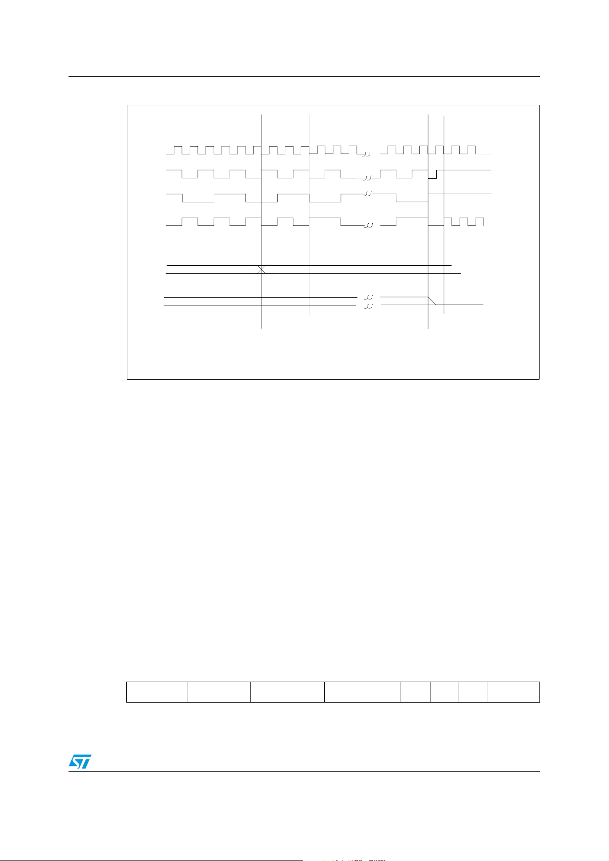
Figure 9. Functional Description
WATCHDOG STATUS REGISTER (WDGSR)
f
CPU
RESET
WATCHDOG CONTROL REGISTER (WDGCR)
MSB
WDGA
7-BIT DOWNCOUNTER
CLOCK DIVIDER
÷12288
LSB
WDGF
The Watchdog delay time is defined by bits 5-0 of the Watchdog register; bit 6 must always
be set in order to avoid generating an immediate reset. Conversely, this can be used to
generate a software reset (bit 7 = 1, bit 6 = 0).
The Watchdog must be reloaded before bit 6 is decremented to “0” to avoid a Reset.
Following a Reset, the Watchdog register will contain 7Fh (bits 0-7).
If the circuit is not used as a Watchdog (i.e. bit 7 is never set), bits 6 to 0 may be used as a
simple 7-bit timer, for instance as a real time clock. Since no reset will be generated under
these conditions, the Watchdog control register must be monitored by software.
23/127

Clocks, Reset, Interrupts & Power saving modes L9805E
A flag in the watchdog status register indicates if the last reset is a watchdog reset or not,
before clearing by a write of this register.
3.3.4 Register Description
Watchdog Control Register
(WDGCR)
Register Address: 002Ah — Read/Write
Reset Value: 0111 1111 (7Fh)
7 0
WDGA T6 T5 T4 T3 T2 T1 T0
b7 = WDGA: Activation bit.
This bit is set by software and only cleared by hardware after a reset. When WDGA = 1, the
watchdog can generate a reset.
0: Watchdog disabled
1: Watchdog enabled.
b6-0 =T6-T0: 7 bit timer (Msb to Lsb)
These bits contain the decremented value. A reset is produced when it rolls over from 40h to
3Fh (T6 become cleared).
Watchdog Status Register
(WDGSR)
Register Address: 002Bh — Read/Write
Reset Value
7 0
-- ----- WDGF
(*)
: 0000 0000 (00h)
b7-1 = not used
b0 = WDGF: Watchdog flag. Set by a Watchdog Reset, cleared by software (writing zero) or
Power On / Low Voltage Reset. This flag is useful for distinguishing Power On / Low Voltage
Reset and Watchdog Reset.
(*): Except in the case of Watchdog Reset.
3.4 Miscellaneous Register
(MISCR)
The Miscellaneous register allows the user to select the Slow operating mode and to set the
clock division prescaler factor. Bits 3, 4 determine the signal conditions which will trigger an
interrupt request on I/O pins having interrupt capability.
Register Address: 0020h — Read/Write
24/127
L9805E Clocks, Reset, Interrupts & Power saving modes
Reset Value:0000 0000 (00h)
- - - b4b3 b2 b1b0
b0 - Slow Mode Select
0- Normal mode - Oscillator frequency / 2 (Reset state)
1- Slow mode (Bits b1 and b2 define the prescaler factor)
b1, b2 - CPU clock prescaler for Slow Mode
b2 b1 Option
0 0 Oscillator frequency / 4
1 0 Oscillator frequency / 8
0 1 Oscillator frequency / 16
1 1 Oscillator frequency / 32
b3, b4 - External Interrupt Option
b4 b3 Option
0 0 Falling edge and low level (Reset state)
1 0 Falling edge only
0 1 Rising edge only
1 1 Rising and Falling edge
The selection issued from b3/b4 combination is applied to PA[0]..PA[7],PB0,PB1 external
interrupt. The selection can be made only if I bit in CC register is reset (interrupt enabled).
b3, b4 can be written only when the Interrupt Mask (I) of the CC (Condition Code) register is
set to 1.
b5,b6,b7 = not used
3.5 Reset
3.5.1 Introduction
There are four sources of Reset:
– NRESET pin (external source)
– Power-On Reset / Low Voltage Detection (Internal source)
– WATCHDOG (Internal Source)
– SAFEGUARD (Internal source)
The Reset Service Routine vector is located at address FFFEh-FFFFh.
25/127

Clocks, Reset, Interrupts & Power saving modes L9805E
3.5.2 External Reset
The NRESET pin is both an input and an open-drain output with integrated pull-up resistor.
When one of the internal Reset sources is active, the Reset pin is driven low to reset the
whole application.
3.5.3 Reset Operation
The duration of the Reset condition, which is also reflected on the output pin, is fixed at 4096
internal CPU Clock cycles. A Reset signal originating from an external source must have a
duration of at least 1.5 internal CPU Clock cycles in order to be recognised. At the end of the
Power-On Reset cycle, the MCU may be held in the Reset condition by an External Reset
signal. The NRESET pin may thus be used to ensure V
has risen to a point where the
DD
MCU can operate correctly before the user program is run. Following a Power-On Reset
event, or after exiting Halt mode, a 4096 CPU Clock cycle delay period is initiated in order to
allow the oscillator to stabilise and to ensure that recovery has taken place from the Reset
state.
During the Reset cycle, the device Reset pin acts as an output that is pulsed low. In its high
state, an internal pull-up resistor of about 300KΩ is connected to the Reset pin. This resistor
can be pulled low by external circuitry to reset the device.
3.5.4 Power-on Reset - Low Voltage Detection
The POR/LVD function generates a static reset when the supply voltage is below a
reference value. In this way, the Power-On Reset and Low Voltage Reset function are
provided, in order to keep the system in safe condition when the voltage is too low.
The Power-Up and Power-Down thresholds are different, in order to avoid spurious reset
when the MCU starts running and sinks current from the supply.
The LVD reset circuitry generates a reset when V
–V
ResetON
–V
ResetOFF
when V
DD
is rising
when VDD is falling
is below:
DD
The POR/LVD function is explained in Figure 11.
Power-On Reset activates the reset pull up transistor performing a complete chip reset. In
the same way a reset can be triggered by the watchdog, by the safeguard or by external low
level at NRESET pin. An external capacitor connected between NRESET and ground can
extend the power on reset period if required.
26/127
L9805E Clocks, Reset, Interrupts & Power saving modes
Figure 10. Power Up/Down behaviour
V
DD
5V
V
Reset ON
V
Reset OFF
V
Reset UD
t
POR/LVD
5V
Figure 11. Reset Block Diagram
V
DD
NRESET
Oscillator
Signal
300K
= undefined value
to ST7
CLK
Reset
t
Internal
RESET
RESET
Counter
Watchdog Reset
Safeguard Reset
POR/LVD Reset
27/127
Clocks, Reset, Interrupts & Power saving modes L9805E
3.6 Interrupts
A list of interrupt sources is given in Tab le 4 below, together with relevant details for each
source. Interrupts are serviced according to their order of priority, starting with I0, which has
the highest priority, and so to I12, which has the lowest priority.
The following list describes the origins for each interrupt level:
– I0 connected to Ports PA0-PA7, PB0-PB1
– I1 connected to CAN
– I2 connected to Power Diagnostics
– I3 connected to Output Compare of Timer 1
– I4 connected to Input Capture of TImer 1
– I5 connected to Timer 1 Overflow
– I6 connected to Output Compare of Timer 2
– I7 connected to Input Capture of TImer 2
– I8 connected to Timer 2 Overflow
– I9 connected to ADC End Of Conversion
– I10 connected to PWM 1 Overflow
– I11 connected to PWM 2 Overflow
– I12 connected to EEPROM
Exit from Halt mode may only be triggered by an External Interrupt on one of the following
ports: PA0-PA7 (I0), PB0-PB1 (I0), or by an Internal Interrupt coming from CAN peripheral
(I1).
If more than one input pin of a group connected to the same interrupt line are selected
simultaneously, the OR of this signals generates the interrupt.
Table 4. Interrupt Mapping
Reset N/A N/A - FFFEh-FFFFh
Software N/A N/A - FFFCh-FFFDh
Ext. Interrupt (Ports PA0-PA7, PB0PB1)
Receive Interrupt Flag
Error Interrupt Pending EPND
Power Bridge Short Circuit
Overtemperature OVT
Output Compare 1
Output Compare 2 OCF2_1
Input Capture 1
Input Capture 2 ICF2_1
Interrupts Register Flag name
N/A N/A I0 FFFAh-FFFBh
RXIFi
CAN Status
Bridge Control
Status
Timer 1 Status
Timer 1 Status
SC
OCF1_1
ICF1_1
Interrupt
source
I1 FFF8h-FFF9hTransmit Interrupt Flag TXIF
I2 FFF6h-FFF7h
I3 FFF4h-FFF5h
I4 FFF2h-FFF3h
Vector
Address
28/127
L9805E Clocks, Reset, Interrupts & Power saving modes
Table 4. Interrupt Mapping (continued)
Interrupts Register Flag name
Interrupt
source
Vector
Address
Timer Overflow Timer 1 Status TOF_1 I5 FFF0h-FFF1h
Output Compare 1
Timer 2 Status
OCF1_2
I6 FFEEh-FFEFh
Output Compare 2 OCF2_2
Input Capture 1
Timer 2 Status
ICF1_2
I7 FFECh-FFEDh
Input Capture 2 ICF2_2
Timer Overflow Timer 2 Status TOF_2 I8 FFEAh-FFEBh
ADC End Of Conversion ADC Control EOC I9 FFE8h-FFE9h
PWM 1 Overflow N/A N/A I10 FFE6h-FFE7h
PWM 2 Overflow N/A N/A I11 FFE4h-FFE5h
EEPROM Programming EEPROM Control E2ITE I12 FFE2h-FFE3h
Figure 12. Interrupt Processing Flowchart
INTERRUPT
TRAP
Y
I BIT = 1
FETCH NEXT INSTRUCTION
OF APPROPRIATE INTERRUPT
SERVICE ROUTINE
EXECUTE INSTRUCTION
Y
N
PUSH
PC,X,A,CC
ONTO STACK
SET I BIT TO 1
LOAD PC
WUTH APPROPRIATE
INTERRUPT VECTOR
(1)
Note: 1 See Ta bl e 4
29/127
Clocks, Reset, Interrupts & Power saving modes L9805E
3.7 Power Saving Modes
3.7.1 Introduction
There are three Power Saving modes. The Slow Mode may be selected by setting the
relevant bits in the Miscellaneous register as detailed in Section 3.4. Wait and Halt modes
may be entered using the WFI and HALT instructions.
3.7.2 Slow Mode
In Slow mode, the oscillator frequency can be divided by 4, 8, 16 or 32 rather than by 2. The
CPU and peripherals (except CAN, see Note) are clocked at this lower frequency. Slow
mode is used to reduce power consumption.
Note: Before entering Slow mode and to guarantee low power operations, the CAN Controller
must be placed by software in STANDBY mode.
3.7.3 Wait Mode
Wait mode places the MCU in a low power consumption mode by stopping the CPU. All
peripherals remain active. During Wait mode, the I bit (CC Register) is cleared, so as to
enable all interrupts. All other registers and memory remain unchanged. The MCU will
remain in Wait mode until an Interrupt or Reset occurs, whereupon the Program Counter
branches to the starting address of the Interrupt or Reset Service Routine.
The MCU will remain in Wait mode until a Reset or an Interrupt (coming from CAN, Timers 1
& 2, EEPROM, ADC, PWM 1 & 2, I/O ports peripherals and Power Bridge) occurs, causing
its wake-up.
Refer to Figure 12 below.
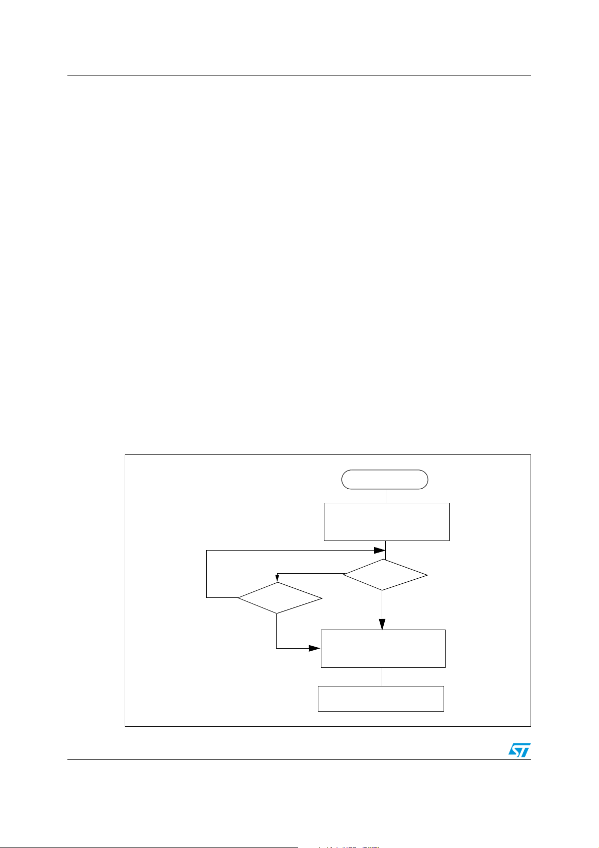
Figure 13. Wait Mode Flow Chart
N
INTERRUPT
WAIT INSTRUCTION
OSCILLATOR
PERIPH. CLOCK
CPU CLOCK
I-BIT
N
Y
OSCILLATOR
PERIPH. CLOCK
CPU CLOCK
I-BIT
FETCH RESET VECTOR
OR SERVICE INTERRUPT
RESET
Y
ON
ON
ON
OFF
CLEARED
ON
ON
SET
30/127

L9805E Clocks, Reset, Interrupts & Power saving modes
3.7.4 Halt Mode
The Halt mode is the MCU lowest power consumption mode. The Halt mode is entered by
executing the HALT instruction. The internal oscillator is then turned off, causing all internal
processing to be stopped, including the operation of the on-chip peripherals.
When entering Halt mode, the I bit in the CC Register is cleared so as to enable External
Interrupts. If an interrupt occurs, the CPU becomes active.
The MCU can exit the Halt mode upon reception of either an external interrupt (I0), a
internal interrupt coming from the CAN peripheral (I1) or a reset. The oscillator is then
turned on and a stabilisation time is provided before releasing CPU operation. The
stabilisation time is 4096 CPU clock cycles.
After the start up delay, the CPU continues operation by servicing the interrupt which wakes
it up or by fetching the reset vector if a reset wakes it up.
Note: The Halt mode cannot be used when the watchdog or the Safeguard are enabled, if the
HALT instruction is executed while the watchdog or safeguard system are enabled, a reset is
automatically generated thus resetting the entire MCU.
Halt Mode affects only the digital section of the device. All the analog circuit remain in their
status, including ADC, voltage regulators, bus transceivers and power bridge.
Figure 14. Halt Mode Flow Chart
N
EXTERNAL
INTERRUPT
Y
N
HALT INSTRUCTION
OSCILLATOR
PERIPH. CLOCK
CPU CLOCK
I-BIT
OSCILLATOR
PERIPH. CLOCK
CPU CLOCK
I-BIT
4096 CPU CLOCK
CYCLES DELAY
FETCH RESET VECTOR
OR SERVICE INTERRUPT
RESET
Y
OFF
OFF
OFF
CLEARED
ON
ON
ON
SET
31/127

Voltage Regulator L9805E
4 Voltage Regulator
4.1 Introduction
The on chip voltage regulator provides two regulated voltage, nominally 5V both. VCC
supplies ADC and the analog periphery and VDD supplies the microcontroller and logic
parts. These voltage are available at pins VDD and VCC to supply external components and
connects a capacitors to optimize EMI performance. A pre-regulator circuit allows to connect
external tantalum capacitors to a lower (10V) voltage (VB2 pin).
4.1.1 Functional Description
The main supply voltage is taken from VB1 pin. A voltage pre-regulator provides the
regulated voltage on pin VB2. VB2 is the supply for the digital and analog regulators. The
block diagram shows the connections between the regulators and the external pins.
In order to prevent negative spikes on the battery line to propagate on the internal supply
generating spurious reset, a series diode supply VB1 pin is recommended.
Figure 15. Voltage regulation block diagram
Battery
VB1
VB2
PRE-REGULATOR
ANALOG
VOLTAGE
REGULATOR
DIGITAL
VOLTAGE
REGULATOR
ADC
force
sense
VCC
AGND
VDD
GND
32/127

L9805E Voltage Regulator
4.2 Digital Section Power Supply
The digital supply voltage VDD is available at pin number 42 and 9. The digital ground GND
is available at pin number 43 and 12.
Pin 42 and 43 are the actual voltage regulator output and external loads must be supply by
these pin. The 100nF compensation capacitor should be connected as close as possible to
pin 42 and 43.
Pin number 9 and 12 provide an external access to the internal oscillator supply.
Resonator’s capacitors should be grounded on pin 12.
The application board can improve noise reduction in the chip connecting directly pin 42 to
pin 9 and pin 43 to pin 12 using traces as short as possible. An additional capacitor mounted
close to pin 9 and 12 can lead additional improvement.
4.2.1 VDD Short Circuit Protection
The output current of the digital voltage regulator is controlled by a circuit that limits it to a
maximum value (I
starts falling down. External loads must be chosen taking in account this maximum current
capability of the regulator.
MAXVDD
). When the output current exceeds this value the VDD voltage
4.3 Analog Section Power Supply
The analog supply voltage is available on VCC pin. The external 100nF compensation
capacitor should be placed as close as possible to this pin and AGND pin.
VCC is the reference voltage for the AD conversion and must be used to supply ratiometric
sensors feeding AD inputs. Any voltage drop between VCC pin and the sensor supply pin on
the application board, will cause the ADC to be inaccurate when reading the sensor’s
output.
4.3.1 VCC Short Circuit Protection
The output current of the analog voltage regulator is controlled by a circuit that limits it to a
maximum value (I
starts falling down. External loads must be chosen taking in account this maximum current
capability of the regulator.
Warning: The pin VB2 is not short circuit protected so a short circuit
MAXVCC
). When the output current exceeds this value the VCC voltage
on this pin will destroy the device.
33/127

On-Chip Peripherals L9805E
5 On-Chip Peripherals
5.1 I/O Ports
5.1.1 Introduction
The internal I/O ports allow the transfer of data through digital inputs and outputs, the
interrupt generation coming from an I/O and for specific pins, the input/output of alternate
signals for the on-chip peripherals (TIMERS...).
Each pin can be programmed independently as digital input (with or without interrupt
generation) or digital output.
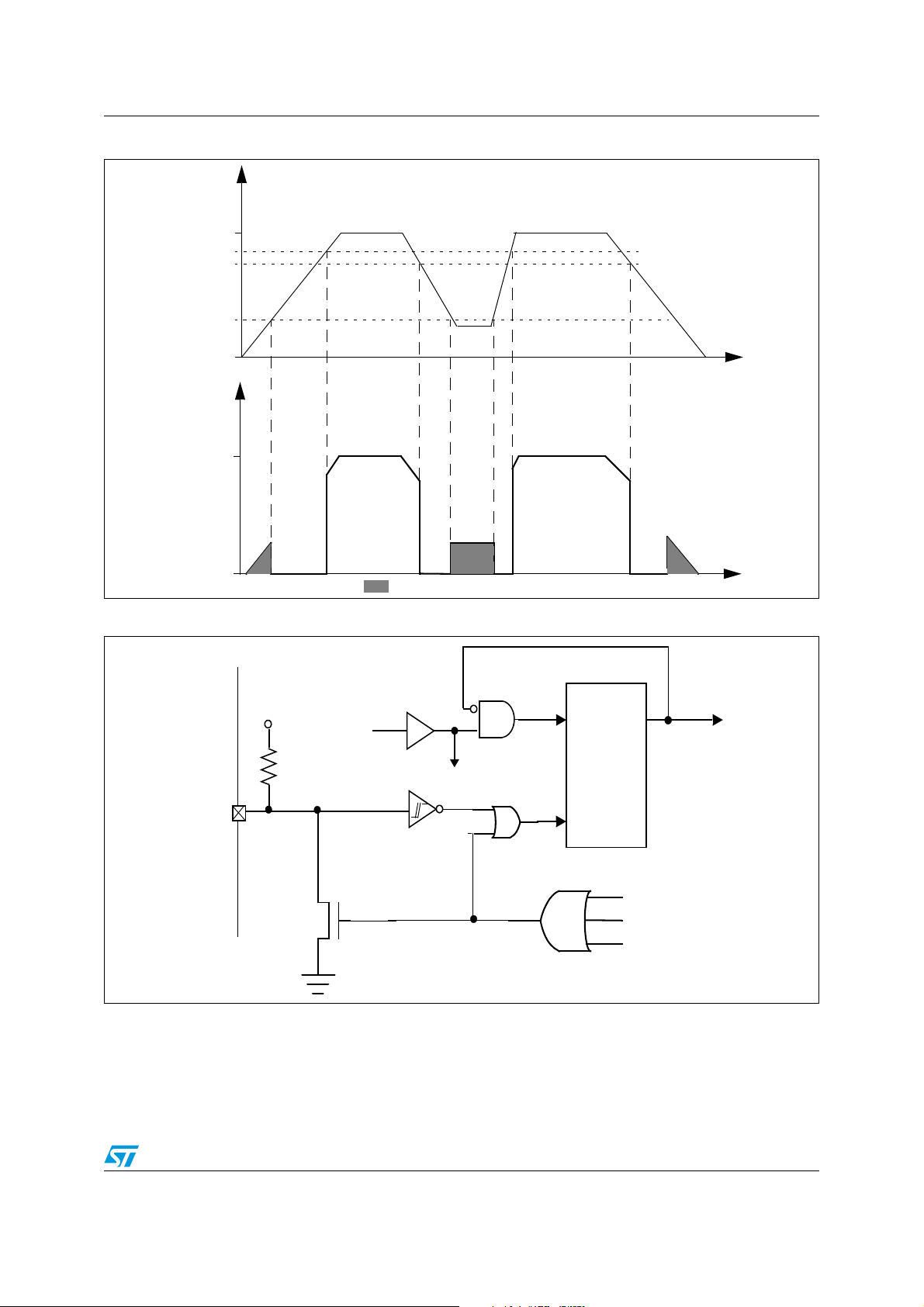
5.1.2 Functional Description
Each port has 2 main registers:
– Data Register (DR)
– Data Direction Register (DDR)
and one optional register:
– Option Register (OR)
Each I/O pin may be programmed using the corresponding register bits in the DDR and OR
registers: bit X corresponding to pin X of the port. The same correspondence is used for the
DR register.
The following description takes into account the OR register, (for specific ports which do not
provide this register refer to the I/O Port Implementation section). The generic I/O block
diagram is shown in Figure 16.
Input Modes
The input configuration is selected by clearing the corresponding DDR register bit.
In this case, reading the DR register returns the digital value applied to the external I/O pin.
Different input modes can be selected by software through the OR register.
Note: 1 1. Writing the DR register modifies the latch value but does not affect the pin status.
2 2. When switching from input to output mode, the DR register has to be written first to drive
the correct level on the pin as soon as the port is configured as an output.
3 3. Do not use read/modify/write instructions (BSET or BRES) to modify the DR register
External interrupt function
When an I/O is configured as Input with Interrupt, an event on this I/O can generate an
external interrupt request to the CPU.
Each pin can independently generate an interrupt request. The interrupt sensitivity is
independently programmable using the sensitivity bits in the Miscellaneous register.
Each external interrupt vector is linked to a dedicated group of I/O port pins (see pinout
description and interrupt section). If several input pins are selected simultaneously as
interrupt source, these are logically NANDed. For this reason if one of the interrupt pins is
tied low, it masks the other ones.
34/127

L9805E On-Chip Peripherals
In case of a floating input with interrupt configuration, special care must be taken when
changing the configuration (see Figure 17).
The external interrupts are hardware interrupts, which means that the request latch (not
accessible directly by the application) is automatically cleared when the corresponding
interrupt vector is fetched. To clear an unwanted pending interrupt by software, the
sensitivity bits in the Miscellaneous register must be modified.
Output Mode
The output configuration is selected by setting the corresponding DDR register bit. In this
case, writing the DR register applies this digital value to the I/O pin through the latch. Then
reading the DR register returns the previously stored value.
Two different output modes can be selected by software through the OR register: Output
push-pull and open-drain.
DR register value and output pin status:
DR Push-Pull Open-drain
0 Vss Vss
1 V
DD Floating
Alternate function
When an on-chip peripheral is configured to use a pin, the alternate function is automatically
selected.
This alternate function takes priority over the standard I/O programming.
When the signal is coming from an on-chip peripheral, the I/O pin is automatically
configured in output mode (push-pull or open drain according to the peripheral).
When the signal is going to an on-chip peripheral, the I/O pin must be configured in input
mode. In this case, the pin state is also digitally readable by addressing the DR register.
Note: Input pull-up configuration can cause unexpected value at the input of the alternate
peripheral input. When an on-chip peripheral use a pin as input and output, this pin has to
be configured in input floating mode.
35/127

On-Chip Peripherals L9805E
Figure 16. I/O Port General Block Diagram
REGISTER
ACCESS
DATA BUS
OR SEL
DDR SEL
DR SEL
EXTERNAL
INTERRUPT
SOURCE (eix)
DR
DDR
OR
POLARITY
SELECTION
ALTERNATE
OUTPUT
ALTERNATE
ENABLE
If implemented
1
0
FROM
OTHER
BITS
1
0
PULL-UP
CONFIGURATION
N-BUFFER
V
CMOS
SCHMITT
TRIGGER
DD
P-BUFFER
(see table below)
PULL-UP
(see table below)
V
DD
PAD
DIODES
(see table below)
ANALOG
INPUT
ALTERNATE
INPUT
Table 5. I/O Port Mode Options
Configuration Mode Pull-Up P-Buffer
Floating with/without Interrupt Off
Input
Pull-up with/without Interrupt On
Push-pull
Output
Open Drain (logic level) Off
True Open Drain NI NI NI (see note)
Legend: NI - not implemented
Off - implemented not activated
On - implemented and activated
Note: The diode to V
the pad and V
Diodes
to V
to VSS
DD
Off
On
On
On
Off
is not implemented in the true open drain pads. A local protection between
DD
is implemented to protect the device against positive stress.
SS
36/127

L9805E On-Chip Peripherals
Table 6. I/O Port Configurations
Hardware Configuration
NOT IMPLEMENTED IN
TRUE OPEN DRAIN
I/O PORTS
1)
INPUT
PAD
V
DD
R
PU
PULL-UP
CONFIGURATION
INTERRUPT
CONFIGURATION
FROM
OTHER
PINS
DR REGISTER ACCESS
DR
REGISTER
POLARITY
SELECTION
W
R
DATA BUS
ALTERNATE INPUT
EXTERNAL INTERRUPT
SOURCE (ei
ANALOG INPUT
)
x
NOT IMPLEMENTED IN
TRUE OPEN DRAIN
2)
I/O PORTS
OPEN-DRAIN OUTPUT
NOT IMPLEMENTED IN
TRUE OPEN DRAIN
2)
I/O PORTS
PUSH-PULL OUTPUT
PAD
PAD
V
DD
R
PU
ENABLE OUTPUT
V
DD
R
PU
ENABLE OUTPUT
DR REGIST ER ACCESS
DR
REGISTER
ALTERNATEALTERNATE
DR REGIST ER ACCESS
DR
REGISTER
ALTERNATEALTERNATE
R/W
R/W
DATA BUS
DATA BUS
Note: 1 1. When the I/O port is in input configuration and the associated alternate function is
enabled as an output, reading the DR register will read the alternate function output status.
2 2. When the I/O port is in output configuration and the associated alternate function is
enabled as an input, the alternate function reads the pin status given by the DR register
content.
Caution: The alternate function must not be activated as long as the pin is configured as input with
interrupt, in order to avoid generating spurious interrupts.
Warning: The analog input voltage level must be within the limits
stated in the absolute maximum ratings.
The hardware implementation on each I/O port depends on the settings in the DDR and OR
registers and specific feature of the I/O port.Switching these I/O ports from one state to
another should be done in a sequence that prevents unwanted side effects. Recommended
safe transitions are illustrated in Figure 17. Other transitions are potentially risky and should
37/127

On-Chip Peripherals L9805E
be avoided, since they are likely to present unwanted side-effects such as spurious
interrupt generation.
Figure 17. Interrupt I/O Port State Transitions
01
INPUT
floating/pull-up
interrupt
00
INPUT
floating
(reset state)
10
OUTPUT
open-drain
XX
11
OUTPUT
push-pull
= DDR, OR
I/O Port Implementation
The I/O port register configurations are resumed as following.
Port PA(7:0), Port PB(2:0)
DDR OR MODE
00
01
no interrupt (pull-up enabled)
interrupt (pull-up enabled)
1 0 Open-Drain output
1 1 Push-Pull output
RESET status: DR=0, DDR=0 and OR=0 (Input mode, no interrupt).
These ports offer interrupt capabilities.
input
input
38/127

L9805E On-Chip Peripherals
Dedicated Configurations
Table 7. Port A Configuration
PORT A
I / O Function
Input Output Alternate Interrupt
PA0 triggered with pull-up push-pull/open drain
PA1 triggered with pull-up push-pull/open drain
PA2 triggered with pull-up push-pull/open drain
PA3 triggered with pull-up push-pull/open drain
PA4 triggered with pull-up push-pull/open drain
PA5 triggered with pull-up push-pull/open drain
PA6 triggered with pull-up push-pull/open drain
PA7 triggered with pull-up push-pull/open drain
Table 8. Port B Configuration
.
I / O Function
PORT B
Input Output Alternate Interrupt
PB0 triggered with pull-up push-pull/open drain
OCMP2_1: Output Compare
#2 Timer 1
OCMP1_1: Output Compare
#1 Timer 1
ICAP2_1: Input Capture #2
Timer 1
ICAP1_1: Input Capture #1
Timer 1
EXTCLK_1: External Clock
Timer 1
OCMP2_2: Output Compare
#2 Timer 2
OCMP1_2: Output Compare
#1 Timer 2
ICAP2_2: Input Capture #2
Timer 2
ICAP1_2: Input Capture #1
Timer 2
wake-up interrupt
(I0)
wake-up interrupt
(I0)
wake-up interrupt
(I0)
wake-up interrupt
(I0)
wake-up interrupt
(I0)
wake-up interrupt
(I0)
wake-up interrupt
(I0)
wake-up interrupt
(I0)
wake-up interrupt
(I0)
PB1 triggered with pull-up push-pull/open drain
(1)
PB2
1. The PB2 bit is not connected to the external. It must be configured as an Input without interrupt, to be used only as an
alternate function.
Not connected to pad Not connected to pad PWMI: PWM input
EXTCLK_2: External Clock
Timer 2
wake-up interrupt
(I0)
39/127

On-Chip Peripherals L9805E
Figure 18. Ports PA0-PA7, PB0-PB1I
Alternate enable
Alternate
output
1
M
U
X
0
VDD
P-BUFFER
Data Bus
Alternate input
DR
latch
DDR
latch
OR
latch
OR SEL
DDR SEL
DR SEL
Alternate
enable
Pull-up
condition
PAD
N-BUFFER
1
M
U
X
0
Alternate
enable
digital enable
GND
Interrupt
from
other
bits
40/127

L9805E On-Chip Peripherals
5.1.3 Register Description
Data registers
(PADR)
Port A: 0000h
Read/Write
Reset Value: 0000 0000 (00h)
7 0
MSB LSB
(PBDR)
Port B: 0004h
Read/Write
Reset Value: 0000 0000 (00h)
7 0
MSB 0 0 0 0 LSB
Data direction registers
(PADDR)
Port A: 0001h
Read/Write
Reset Value: 0000 0000 (00h) (input mode)
7 0
MSB LSB
(PBDDR)
Port B: 0005h
Read/Write
Reset Value: 0000 0000 (00h) (input mode)
7 0
MSB 0 0 0 0 LSB
41/127

On-Chip Peripherals L9805E
Option registers
(PAOR)
Port A: 0002h
Read/Write
Reset Value: 0000 0000 (00h) (no interrupt)
7 0
MSB LSB
(PBOR)
Port B: 0006h
Read/Write
Reset Value: 0000 0000 (00h) (no interrupt)
7 0
MSB 0 0 0 0 LSB
5.2 16-Bit Timer
5.2.1 Introduction
The timer consists of a 16-bit free-running counter driven by a programmable prescaler.
It may be used for a variety of purposes, including pulse length measurement of up to two
input signals (input capture) or generation of up to two output waveforms (output compare
and PWM).
Pulse lengths and waveform periods can be modulated from a few microseconds to several
milliseconds using the timer prescaler and the CPU clock prescaler.
42/127

L9805E On-Chip Peripherals
5.2.2 Main Features
● Programmable prescaler: f
● Overflow status flag and maskable interrupt
● External clock input (must be at least 4 times slower than the CPU clock speed) with
divided by 2, 4 or 8.
cpu
the choice of active edge
● Output compare functions with
– 2 dedicated 16-bit registers
– 2 dedicated programmable signals
– 2 dedicated status flags
– 1 dedicated maskable interrupt
● Input capture functions with
– 2 dedicated 16-bit registers
– 2 dedicated active edge selection signals
– 2 dedicated status flags
– 1 dedicated maskable interrupt
● Pulse width modulation mode (PWM)
● One pulse mode
● 5 alternate functions on I/O ports
The Block Diagram is shown in Figure 19 on page 44.
Note: Some external pins are not available on all devices. Refer to the device pin out description.
5.2.3 Functional Description
Counter
The main block of the Programmable Timer is a 16-bit free running upcounter and its
associated 16-bit registers. The 16-bit registers are made up of two 8-bit registers called
high & low.
Counter Register (CR):
– Counter High Register (CHR) is the most significant byte (MS Byte).
– Counter Low Register (CLR) is the least significant byte (LS Byte).
Alternate Counter Register (ACR)
– Alternate Counter High Register (ACHR) is the most significant byte (MS Byte).
– Alternate Counter Low Register (ACLR) is the least significant byte (LS Byte).
These two read-only 16-bit registers contain the same value but with the difference that
reading the ACLR register does not clear the TOF bit (Timer overflow flag), located in the
Status register (SR). (See note at the end of paragraph titled 16-bit read sequence).
Writing in the CLR register or ACLR register resets the free running counter to the FFFCh
value.
Both counters have a reset value of FFFCh (this is the only value which is reloaded in the
16-bit timer). The reset value of both counters is also FFFCh in One Pulse mode and PWM
mode.
43/127

On-Chip Peripherals L9805E
The timer clock depends on the clock control bits of the CR2 register, as illustrated in
Table 9: Clock Control Bits. The value in the counter register repeats every 131072, 262144
or 524288 CPU clock cycles depending on the CC[1:0] bits.
The timer frequency can be f
CPU
/2, f
Figure 19. Timer Block Diagram
CPU CLOCK
8-bit
buffer
16 BIT
COUNTER
COUNTER
DETECT
CIRCUIT
8 low
16
16
OUTPUT COMPARE
EXCLK
8 high
EXEDG
1/2
1/4
1/8
CC1 CC0
FREE RUNNING
ALTERNATE
REGISTER
OVERFLOW
/4, f
CPU
/8 or an external frequency.
CPU
ST7 INTERNAL BUS
MCU-PERIPHERAL INTERFACE
8
88 8
high
low
high
low
OUTPUT
COMPARE
REGISTER
1
OUTPUT
COMPARE
REGISTER
2
TIMER INTERNAL BUS
16 16
CIRCUIT
8
high
low
INPUT
CAPTURE
REGISTER
1
EDGE DETECT
8 8 8
high
low
INPUT
CAPTURE
REGISTER
2
16
CIRCUIT1
16
ICAP1
ICF2ICF1 000OCF2OCF1 TOF
TIMER INTERRUPT
SR
CR1
6
OC2E
EDGE DETECT
CIRCUIT2
PWMOC1E
OPMFOLV2ICIE OLVL1IEDG1OLVL2FOLV1OCIE TOIE
LATCH1
LATCH2
ICAP2
OCMP1
OCMP2
EXEDG
IEDG2CC0CC1
CR2
44/127

L9805E On-Chip Peripherals
16-bit read sequence: (from either the Counter Register or the Alternate Counter
Register).
Beginning of the sequence
At t0
At t0 +∆t
Sequence completed
Read MSB
Other
instructions
Read LSB
LSB is buffered
Returns the buffered
LSB value at t0
The user must read the MSB first, then the LSB value is buffered automatically.
This buffered value remains unchanged until the 16-bit read sequence is completed, even if
the user reads the MSB several times.
After a complete reading sequence, if only the CLR register or ACLR register are read, they
return the LSB of the count value at the time of the read.
An overflow occurs when the counter rolls over from FFFFh to 0000h then:
● The TOF bit of the SR register is set.
● A timer interrupt is generated if:
– TOIE bit of the CR1register is set and
– I bit of the CCR register is cleared.
If one of these conditions is false, the interrupt remains pending to be issued as soon as
they are both true.
Clearing the overflow interrupt request is done by:
1. Reading the SR register while the TOF bit is set.
2. An access (read or write) to the CLR register.
Note: The TOF bit is not cleared by accesses to ACLR register. This feature allows simultaneous
use of the overflow function and reads of the free running counter at random times (for
example, to measure elapsed time) without the risk of clearing the TOF bit erroneously.
The timer is not affected by WAIT mode.
In HALT mode, the counter stops counting until the mode is exited. Counting then resumes
from the previous count (MCU awakened by an interrupt) or from the reset count (MCU
awakened by a Reset).
External Clock
The external clock (where available) is selected if CC0=1 and CC1=1 in CR2 register.
The status of the EXEDG bit determines the type of level transition on the external clock pin
EXCLK that will trigger the free running counter.
The counter is synchronised with the falling edge of the internal CPU clock.
At least four falling edges of the CPU clock must occur between two consecutive active
edges of the external clock; thus the external clock frequency must be less than a quarter of
the CPU clock frequency.
45/127

On-Chip Peripherals L9805E
Figure 20. Counter Timing Diagram, internal clock divided by 2
CPU CLOCK
INTERNAL RESET
TIMER CLOCK
COUNTER REGISTER
OVERFLOW FLAG TOF
FFFD FFFE FFFF 0000 0001 0002 0003
Figure 21. Counter Timing Diagram, internal clock divided by 4
CPU CLOCK
INTERNAL RESET
TIMER CLOCK
COUNTER REGISTER
OVERFLOW FLAG TOF
FFFC FFFD 0000 0001
Figure 22. Counter Timing Diagram, internal clock divided by 8
CPU CLOCK
INTERNAL RESET
TIMER CLOCK
COUNTER REGISTER
OVERFLOW FLAG TOF
FFFC FFFD
Input Capture
In this section, the index, i, may be 1 or 2
The two input capture 16-bit registers (ICR1 and ICR2) are used to latch the value of the
free running counter after a transition detected by the ICAPi pin (see figure 5)
.
MS Byte LS Byte
ICRi ICHRi ICLRi
ICRi register is a read-only register.
46/127
0000

L9805E On-Chip Peripherals
The active transition is software programmable through the IEDGi bit of the Control Register
(CRi).
Timing resolution is one count of the free running counter: (
f
CPU/(CC1.CC0)
).
Procedure
To use the input capture function select the following in the CR2 register:
– Select the timer clock (CC1-CC0) (see Table 9: Clock Control Bits).
– Select the edge of the active transition on the ICAP2 pin with the IEDG2 bit.
And select the following in the CR1 register:
– Set the ICIE bit to generate an interrupt after an input capture.
– Select the edge of the active transition on the ICAP1 pin with the IEDG1 bit.
When an input capture occurs:
–ICFi bit is set.
–The ICRi register contains the value of the free running counter on the active
transition on the ICAPi pin (see Figure 23).
– A timer interrupt is generated if the ICIE bit is set and the I bit is cleared in the
CCR register. Otherwise, the interrupt remains pending until both conditions
become true.
Clearing the Input Capture interrupt request is done by:
1. Reading the SR register while the ICFi bit is set.
2. An access (read or write) to the ICLRi register.
Note: After reading the ICHRi register, transfer of input capture data is inhibited until the ICLRi
register is also read.
The ICRi register always contains the free running counter value which corresponds to the
most recent input capture.
During HALT mode, if at least one valid input capture edge occurs on the ICAPi pin, the
input capture detection circuitry is armed. This does not set any timer flags, and does not
“wake-up” the MCU. If the MCU is awoken by an interrupt, the input capture flag will become
active, and data corresponding to the first valid edge during HALT mode will be present.
47/127

On-Chip Peripherals L9805E
Figure 23. Input Capture Block Diagram
ICAP1
ICAP2
EDGE DETECT
CIRCUIT2
ICR2
16-BIT
EDGE DETECT
CIRCUIT1
ICR1
16-BIT FREE RUNNING
COUNTER
Figure 24. Input Capture Timing Diagram
TIMER CLOCK
COUNTER REGISTER
ICAPi PIN
FF01 FF02 FF03
ICIE
(Control Register 1) CR1
IEDG1
(Status Register) SR
ICF2ICF1 000
(Control Register 2) CR2
IEDG2
CC0
CC1
ICAPi FLAG
ICAPi REGISTER
Note: Active edge is rising edge.
FF03
Output Compare
In this section, the index, i, may be 1 or 2 because there are 2 output compare functions in
the 16-bit timer.
This function can be used to control an output waveform or indicate when a period of time
has elapsed.
When a match is found between the Output Compare register and the free running counter,
the output compare function:
– Assigns pins with a programmable value if the OCiE bit is set
– Sets a flag in the status register
– Generates an interrupt if enabled
Two 16-bit registers Output Compare Register 1 (OC1R) and Output Compare Register 2
(OC2R) contain the value to be compared to the counter register each timer clock cycle
48/127

L9805E On-Chip Peripherals
.
MS Byte LS Byte
OCiROCiHR OCiLR
These registers are readable and writable and are not affected by the timer hardware. A
reset event changes the OCiR value to 8000h.
Timing resolution is one count of the free running counter: (
f
CPU/CC[1:0]
).
Procedure
To use the output compare function, select the following in the CR2 register:
– Set the OCiE bit if an output is needed then the OCMPi pin is dedicated to the
output compare i function.
– Select the timer clock (CC[1:0]) (see Table 9: Clock Control Bits).
And select the following in the CR1 register:
– Select the OLVLi bit to applied to the OCMPi pins after the match occurs.
– Set the OCIE bit to generate an interrupt if it is needed.
When a match is found between OCRi register and CR register:
–OCFi bit is set.
–The OCMPi pin takes OLVLi bit value (OCMPi pin latch is forced low during reset).
– A timer interrupt is generated if the OCIE bit is set in the CR1 register and the I bit
is cleared in the CC register (CC).
The OCRi register value required for a specific timing application can be calculated using
the following formula:
∆tf
⋅
∆OCiR
CPU
-----------------------=
PRESC
Where:
∆t = Output compare period (in seconds)
f
= CPU clock frequency (in Hz)
CPU
PRESC = Timer prescaler factor (2, 4 or 8 depending on CC[1:0] bits,
see Table 9: Clock Control Bits)
If the timer clock is an external clock, the formula
is:
∆OCiR = ∆t · f
EXT
Where:
∆t = Output compare period (in seconds)
= External timer clock frequency (in hertz)
f
EXT
Clearing the output compare interrupt request (i.e.clearing the OCFi bit) is done by:
1.
Reading the SR register while the OCFi bit is set.
2. An access (read or write) to the OCiLR register.
49/127

On-Chip Peripherals L9805E
The following procedure is recommended to prevent the OCFi bit from being set between
the time it is read and the write to the OCiR register:
– Write to the OCiHR register (further compares are inhibited).
– Read the SR register (first step of the clearance of the OCFi bit, which may be
already set).
– Write to the OCiLR register (enables the output compare function and clears the
OCFi bit).
Figure 25. Output Compare Block Diagram
16 BIT FREE RUNNING
COUNTER
16-bit
OUTPUT COMPARE
CIRCUIT
16-bit
OC1R Register
16-bit
OC2R Register
OC1E CC0CC1
OC2E
(Control Register 2) CR2
(Control Register 1) CR1
FOLV1
FOLV2
OLVL1OLVL2OCIE
000OCF2OCF1
(Status Register) SR
Latch
1
Latch
2
Figure 26. Output Compare Timing Diagram, Internal Clock Divided by 2
INTERNAL CPU CLOCK
TIMER CLOCK
COUNTER
OUTPUT COMPARE REGISTER
FFFD FFFD FFFE
CPU writes FFFF
FFFF
FFFF
0000FFFC
OCMP1
Pin
OCMP2
Pin
COMPARE REGISTER LATCH
OCFi AND OCMPi PIN (OLVLi=1)
Forced Compare Output capability
When the FOLVi bit is set by software, the OLVLi bit is copied to the OCMPi pin. The OLVi bit
has to be toggled in order to toggle the OCMPi pin when it is enabled (OCiE bit=1). The
OCFi bit is then not set by hardware, and thus no interrupt request is generated.
FOLVLi bits have no effect in either One-Pulse mode or PWM mode.
50/127

L9805E On-Chip Peripherals
One Pulse Mode
One Pulse mode enables the generation of a pulse when an external event occurs. This
mode is selected via the OPM bit in the CR2 register.
The One Pulse mode uses the Input Capture1 function and the Output Compare1 function.
Procedure
To use One Pulse mode:
1. Load the OC1R register with the value corresponding to the length of the pulse (see the
formula in the section).
2. Select the following in the CR1 register:
– Using the OLVL1 bit, select the level to be applied to the OCMP1 pin after the
pulse.
– Using the OLVL2 bit, select the level to be applied to the OCMP1 pin during the
pulse.
– Select the edge of the active transition on the ICAP1 pin with the IEDG1 bit (the
ICAP1 pin must be configured as floating input).
3. Select the following in the CR2 register:
– Set the OC1E bit, the OCMP1 pin is then dedicated to the Output Compare 1
function.
– Set the OPM bit.
– Select the timer clock CC[1:0] (see Table 9: Clock Control Bits).
.
One pulse mode cycle
When
event occurs
on ICAP1
When
Counter
= OCR1
OCMP1 = OLVL2
Counter is reset
to FFFCh
ICF1 bit is set
OCMP1 = OLVL1
Then, on a valid event on the ICAP1 pin, the counter is initialized to FFFCh and the OLVL2
bit is loaded on the OCMP1 pin, the ICF1 bit is set and the value FFFDh is loaded in the
IC1R register.
Because the ICF1 bit is set when an active edge occurs, an interrupt can be generated if the
ICIE bit is set.
Clearing the Input Capture interrupt request (i.e. clearing the ICFi bit) is done in two steps:
1. Reading the SR register while the ICFi bit is set.
2. An access (read or write) to the ICiLR register.
The OC1R register value required for a specific timing application can be calculated using
the following formula:
OCiR Value
tf
----------------------5–=
PRESC
CPU
⋅
Where:
51/127

On-Chip Peripherals L9805E
t = Pulse period (in seconds)
f
= CPU clock frequency (in hertz)
CPU
PRESC = Timer prescaler factor (2, 4 or 8 depending on the CC[1:0] bits,
seeTable 9: Clock Control Bits).
If the timer clock is an external clock the formula is:
Where:
t = Pulse period (in seconds)
f
= External timer clock frequency (in hertz)
EXT
When the value of the counter is equal to the value of the contents of the OC1R register, the
OLVL1 bit is output on the OCMP1 pin (See <Blue HT>Figure 27).
Note: 1 The OCF1 bit cannot be set by hardware in One Pulse mode but the OCF2 bit can generate
an Output Compare interrupt.
2 When the Pulse Width Modulation (PWM) and One Pulse mode (OPM) bits are both set, the
PWM mode is the only active one.
3 If OLVL1=OLVL2 a continuous signal will be seen on the OCMP1 pin.
4 The ICAP1 pin can not be used to perform input capture. The ICAP2 pin can be used to
perform input capture (ICF2 can be set and IC2R can be loaded) but the user must take
care that the counter is reset each time a valid edge occurs on the ICAP1 pin and ICF1 can
also generates interrupt if ICIE is set.
5 When One Pulse mode is used OC1R is dedicated to this mode. Nevertheless OC2R and
OCF2 can be used to indicate that a period of time has elapsed but cannot generate an
output waveform because the OLVL2 level is dedicated to One Pulse mode.
Note: The OCF1 bit cannot be set by hardware in one pulse mode but the OCF2 bit can generate
an Output Compare interrupt.
The ICF1 bit is set when an active edge occurs and can generate an interrupt if the ICIE bit
is set.
When the Pulse Width Modulation (PWM) and One Pulse Mode (OPM) bits are both set, the
PWM mode is the only active one.
Figure 27.
One Pulse Mode Timing
....
COUNTER
ICAP1
OCMP1
Note: IEDG1=1, OCR1=2ED0h, OLVL1=0, OLVL2=1
FFFC FFFD FFFE 2ED0 2ED1 2ED2
OLVL2
compare1
FFFC FFFD
2ED3
OLVL2OLVL1
Pulse Width Modulation Mode
Pulse Width Modulation (PWM) mode enables the generation of a signal with a frequency
and pulse length determined by the value of the OC1R and OC2R registers.
52/127

L9805E On-Chip Peripherals
The Pulse Width Modulation mode uses the complete Output Compare 1 function plus the
OC2R register, and so these functions cannot be used when the PWM mode is activated.
Procedure
To use Pulse Width Modulation mode:
1. Load the OC2R register with the value corresponding to the period of the signal using
the formula in the section.
2. Load the OC1R register with the value corresponding to the period of the pulse if
OLVL1=0 and OLVL2=1, using the formula in the section.
3. Select the following in the CR1 register:
– Using the OLVL1 bit, select the level to be applied to the OCMP1 pin after a
successful comparison with OC1R register.
– Using the OLVL2 bit, select the level to be applied to the OCMP1 pin after a
successful comparison with OC2R register.
4. Select the following in the CR2 register:
– Set OC1E bit: the OCMP1 pin is then dedicated to the output compare 1 function.
– Set the PWM bit.
– Select the timer clock (CC[1:0]) (see Table 9: Clock Control Bits).
If OLVL1=1 and OLVL2=0, the length of the positive pulse is the difference between the
OC2R and OC1R registers.
If OLVL1=OLVL2 a continuous signal will be seen on the OCMP1 pin.
Pulse Width Modulation cycle
When
Counter
= OCR1
When
Counter
= OCR2
OCMP1 = OLVL1
OCMP1 = OLVL2
Counter is reset
to FFFCh
ICF1 bit is set
The OCRi register value required for a specific timing application can be calculated using
the following formula:
tf
⋅
OCiR Value
CPU
--------------------- - 5–=
PRESC
Where:
t = Signal or pulse period (in seconds)
f
= CPU clock frequency (in hertz)
CPU
PRESC = Timer prescaler factor (2, 4 or 8 depending on CC[1:0] bits,
see Table 9: Clock Control Bits
If the timer clock is an external clock the formula is:
OCiR = t · f
EXT
Where:
53/127
-5

On-Chip Peripherals L9805E
t = Signal or pulse period (in seconds)
f
= External timer clock frequency (in hertz)
EXT
The Output Compare 2 event causes the counter to be initialized to FFFCh (See Figure 28
on page 54).
Note: 1 After a write instruction to the OCiHR register, the output compare function is inhibited until
the OCiLR register is also written.
2 The OCF1 and OCF2 bits cannot be set by hardware in PWM mode, therefore the Output
Compare interrupt is inhibited.
3 The ICF1 bit is set by hardware when the counter reaches the OC2R value and can produce
a timer interrupt if the ICIE bit is set and the I bit is cleared.
4 In PWM mode the ICAP1 pin can not be used to perform input capture because it is
disconnected from the timer. The ICAP2 pin can be used to perform input capture (ICF2 can
be set and IC2R can be loaded) but the user must take care that the counter is reset after
each period and ICF1 can also generate an interrupt if ICIE is set.
5 When the Pulse Width Modulation (PWM) and One Pulse mode (OPM) bits are both set, the
PWM mode is the only active one.
Figure 28. Pulse Width Modulation Mode Timing
34E2
COUNTER
OCMP1
FFFC FFFD FFFE 2ED0 2ED1 2ED2 34E2 FFFC
compare2 compare1 compare2
Note: OCR1=2ED0h, OCR2=34E2, OLVL1=0, OLVL2= 1
5.2.4 Register Description
Each Timer is associated with three control and status registers, and with six pairs of data
registers (16-bit values) relating to the two input captures, the two output compares, the
counter and the alternate counter.
CONTROL REGISTER 1 (CR1)
Timer1 Register Address: 0032h
Timer2 Register Address: 0042h
Read/Write
Reset Value: 0000 0000(00h)
7 0
OLVL2
OLVL2OLVL1
ICIE OCIE TOIE FOLV2 FOLV1 OLVL2 IEDG1 OLVL1
54/127

L9805E On-Chip Peripherals
Bit 7 = ICIE Input Capture Interrupt Enable.
0: Interrupt is inhibited.
1: A timer interrupt is generated whenever the ICF1 or ICF2 bits of the SR register are set
Bit 6 = OCIE Output Compare Interrupt Enable.
0: Interrupt is inhibited.
1: A timer interrupt is generated whenever the OCF1 or OCF2 bits of the SR register are
set
Bit 5 = TOIE Timer Overflow Interrupt Enable.
0: Interrupt is inhibited.
1: A timer interrupt is enabled whenever the TOF bit of the SR register is set.
Bit 4 = FOLV2 Forced Output Compare 2.
0: No effect.
1: Forces the OLVL2 bit to be copied to the OCMP2 pin.
Bit 3 = FOLV1 Forced Output Compare 1.
0: No effect.
1: Forces OLVL1 to be copied to the OCMP1 pin.
Bit 2 = OLVL2 Output Level 2.
This bit is copied to the OCMP2 pin whenever a successful comparison occurs with the
OCR2 register. This value is copied to the OCMP1 pin in One Pulse Mode and Pulse Width
Modulation mode.
Bit 1 = IEDG1 Input Edge 1.
This bit determines which type of level transition on the ICAP1 pin will trigger the capture.
0: A falling edge triggers the capture.
1: A rising edge triggers the capture.
Bit 0 = OLVL1 Output Level 1.
The OLVL1 bit is copied to the OCMP1 pin whenever a successful comparison occurs with
the OCR1 register.
CONTROL REGISTER 2 (CR2)
Timer1 Register Address: 0031h
Timer2 Register Address: 0041h
55/127

On-Chip Peripherals L9805E
Read/Write
Reset Value: 0000 0000 (00h)
7 0
OC1E OC2E OPM PWM CC1 CC0 IEDG2 EXEDG
Bit 7 = OC1E Output Compare 1 Enable.
0: Output Compare 1 function is enabled, but the OCMP1 pin is a general I/O.
1: Output Compare 1 function is enabled, the OCMP1 pin is dedicated to the Output
Compare 1 capability of the timer.
Bit 6 = OC2E Output Compare 2 Enable.
0: Output Compare 2 function is enabled, but the OCMP2 pin is a general I/O.
1: Output Compare 2 function is enabled, the OCMP2 pin is dedicated to the Output
Compare 2 capability of the timer.
Bit 5 = OPM One Pulse Mode.
0: One Pulse Mode is not active.
1: One Pulse Mode is active, the ICAP1 pin can be used to trigger one pulse on the
OCMP1 pin; the active transition is given by the IEDG1 bit. The length of the generated
pulse depends on the contents of the OCR1 register.
Bit 4 = PWM Pulse Width Modulation.
0: PWM mode is not active.
1: PWM mode is active, the OCMP1 pin outputs a programmable cyclic signal; the length
of the pulse depends on the value of OCR1 register; the period depends on the value of
OCR2 register.
Bit 3, 2 = CC1-CC0 Clock Control.
The value of the timer clock depends on these bits:
Table 9. Clock Control Bits
CC1 CC0 Timer Clock
00
01
10
1 1 External Clock where available
f
CPU
f
CPU
f
CPU
/ 4
/ 2
/ 8
56/127

L9805E On-Chip Peripherals
Bit 1 = IEDG2 Input Edge 2.
This bit determines which type of level transition on the ICAP2 pin will trigger the capture
0: A falling edge triggers the capture.
1: A rising edge triggers the capture.
Bit 0 = EXEDG External Clock Edge.
This bit determines which type of level transition on the external clock pin EXCLK will trigger
the free running counter.
0: A falling edge triggers the free running counter.
1: A rising edge triggers the free running counter.
STATUS REGISTER (SR)
Timer1 Register Address: 0033h
Timer2 Register Address: 0043h
Read Only
Reset Value: 0000 0000 (00h)
The three least significant bits are not used.
7 0
ICF1 OCF1 TOF ICF2 OCF2
Bit 7 = ICF1 Input Capture Flag 1.
0: No input capture (reset value)
1: An input capture has occurred. To clear this bit, first read the SR register, then read or
write the low byte of the ICR1 (ICLR1) register.
Bit 6 = OCF1 Output Compare Flag 1.
0: No match (reset value)
1: The content of the free running counter has matched the content of the OCR1
register. To clear this bit, first read the SR register, then read or write the low byte of
the OCR1 (OCLR1) register.
Bit 5 = TOF Timer Overflow.
0: No timer overflow (reset value)
1: The free running counter rolled over from FFFFh to 0000h. To clear this bit, first read
the SR register, then read or write the low byte of the CR (CLR) register.
Note: Reading or writing the ACLR register do not clear TOF.
Bit 4 = ICF2 Input Capture Flag 2.
0: No input capture (reset value)
57/127

On-Chip Peripherals L9805E
1: An input capture has occurred.To clear this bit, first read the SR register, then read or
write the low byte of the ICR2 (ICLR2) register.
Bit 3 = OCF2 Output Compare Flag 2.
0: No match (reset value)
1: The content of the free running counter has matched the content of the OCR2 register.
To clear this bit, first read the SR register, then read or write the low byte of the OCR2
(OCLR2) register.
Bit 2-0 = Unused.
INPUT CAPTURE 1 HIGH REGISTER (ICHR1)
Timer1 Register Address: 0034h
Timer2 Register Address: 0044h
Read Only
Reset Value: Undefined
This is an 8-bit read only register that contains the high part of the counter value (transferred
by the input capture 1 event).
7 0
MSB LSB
INPUT CAPTURE 1 LOW REGISTER (ICLR1)
Timer1 Register Address: 0035h
Timer2 Register Address: 0045h
Read Only
Reset Value: Undefined
This is an 8-bit read only register that contains the low part of the counter value (transferred
by the input capture 1 event).
7 0
MSB LSB
58/127

L9805E On-Chip Peripherals
OUTPUT COMPARE 1 HIGH REGISTER (OCHR1)
Timer1 Register Address: 0036h
Timer2 Register Address: 0046h
Read/Write
Reset Value: 1000 0000 (80h)
This is an 8-bit register that contains the high part of the value to be compared to the CHR
register.
7 0
MSB LSB
OUTPUT COMPARE 1 LOW REGISTER (OCLR1)
Timer1 Register Address: 0037h
Timer2 Register Address: 0047h
Read/Write
Reset Value: 0000 0000 (00h)
This is an 8-bit register that contains the low part of the value to be compared to the CLR
register.
7 0
MSB LSB
OUTPUT COMPARE 2 HIGH REGISTER (OCHR2)
Timer1 Register Address: 003Eh
Timer2 Register Address: 004Eh
Read/Write
Reset Value: 1000 0000 (80h)
This is an 8-bit register that contains the high part of the value to be compared to the CHR
register.
.
7 0
MSB LSB
OUTPUT COMPARE 2 LOW REGISTER (OCLR2)
Timer1 Register Address: 003Fh
Timer2 Register Address: 004Fh
Read/Write
Reset Value: 0000 0000 (00h)
This is an 8-bit register that contains the low part of the value to be compared to the CLR register.
.
7 0
MSB LSB
59/127

On-Chip Peripherals L9805E
COUNTER HIGH REGISTER (CHR)
Timer1 Register Address: 0038h
Timer2 Register Address: 0048h
Read Only
Reset Value: 1111 1111 (FFh)
This is an 8-bit register that contains the high part of the counter value.
7 0
MSB LSB
COUNTER LOW REGISTER (CLR)
Timer1 Register Address: 0039h
Timer2 Register Address: 0049h
Read/Write
Reset Value: 1111 1100 (FCh)
This is an 8-bit register that contains the low part of the counter value. A write to this register
resets the counter. An access to this register after accessing the SR register clears the TOF
bit.16-BIT.
7 0
MSB LSB
ALTERNATE COUNTER HIGH REGISTER (ACHR)
Timer1 Register Address: 003Ah
Timer2 Register Address: 004Ah
Read Only
Reset Value: 1111 1111 (FFh)
This is an 8-bit register that contains the high part of the counter value.
.
7 0
MSB LSB
ALTERNATE COUNTER LOW REGISTER (ACLR)
Timer1 Register Address: 003Bh
Timer2 Register Address: 004Bh
Read/Write
Reset Value: 1111 1100 (FCh)
This is an 8-bit register that contains the low part of the counter value. A write to this register
resets the counter. An access to this register after an access to SR register does not clear
the TOF bit in SR register.
60/127

L9805E On-Chip Peripherals
7 0
MSB LSB
INPUT CAPTURE 2 HIGH REGISTER (ICHR2)
Timer1 Register Address: 003Ch
Timer2 Register Address: 004Ch
Read Only
Reset Value: Undefined
This is an 8-bit read only register that contains the high part of the counter value (transferred
by the Input Capture 2 event).
7 0
MSB LSB
INPUT CAPTURE 2 LOW REGISTER (ICLR2)
Timer1 Register Address: 003Dh
Timer2 Register Address: 004Dh
Read Only
Reset Value: Undefined
This is an 8-bit read only register that contains the low part of the counter value (transferred
by the Input Capture 2 event).
7 0
MSB LSB
Table 10. 16-Bit Timer Register Map and Reset Values
Address
(Hex.)
Timer1: 32
Timer2: 42
Timer1: 31
Timer2: 41
Timer1: 33
Timer2: 43SRReset Value
Timer1: 34
Timer2: 44
Timer1: 35
Timer2: 45
Timer1: 36
Timer2: 46
Timer1: 37
Timer2: 47
Register
Name
CR1
Reset Value
CR2
Reset Value
ICHR1
Reset Value
ICLR1
Reset Value
OCHR1
Reset Value
OCLR1
Reset Value
76543210
ICIE
0
OC1E0OC2E
ICF1
0
MSB
-
MSB
-
MSB
-
MSB
-
OCIE
0
0
OCF1
0
TOIE
0
OPM
0
TOF
0
FOLV20FOLV10OLVL20IEDG10OLVL1
PWM
ICF2
------
------
------
------
0
CC1
0
0
OCF2
0
0
CC0
0
-
0
IEDG20EXEDG
0
-
0
-
0
LSB
-
LSB
-
LSB
-
LSB
-
61/127

On-Chip Peripherals L9805E
Table 10. 16-Bit Timer Register Map and Reset Values (continued)
Address
(Hex.)
Timer1: 3E
Timer2: 4E
Timer1: 3F
Timer2: 4F
Timer1: 38
Timer2: 48
Timer1: 39
Timer2: 49
Timer1: 3A
Timer2: 4A
Timer1: 3B
Timer2: 4B
Timer1: 3C
Timer2: 4C
Timer1: 3D
Timer2: 4D
Register
Name
OCHR2
Reset Value
OCLR2
Reset Value
CHR
Reset Value
CLR
Reset Value
ACHR
Reset Value
ACLR
Reset Value
ICHR2
Reset Value
ICLR2
Reset Value
76543210
MSB
-
MSB
-
MSB
1111111
MSB
1111110
MSB
1111111
MSB
1111110
MSB
-
MSB
-
------
------
------
------
LSB
-
LSB
-
LSB
1
LSB
0
LSB
1
LSB
0
LSB
-
LSB
-
5.3 PWM Generator
5.3.1 Introduction
This PWM peripheral includes a 16-bit Pulse Width Modulator (PWM) and a programmable
prescaler able to generate an internal clock with period as long as 128*T
The repetition rate of the 16-Bit PWM output can be defined by a dedicated register
(f
/CYREG); its resolution is defined by the internal clock as per the prescaler
CPU
programming.
Main Features
– Programmable prescaler: f
– 1 control register
– 2 dedicated 16-bit registers for cycle and duty control
– 1 dedicated maskable interrupt
Procedure
To use the pulse width modulation peripheral, the EN_PWM bit in CONREG register must
be set.
Load PS(2:0) in CONREG register to define the programmable prescaler.
Load the CYREG register with the value defining the cycle length (in internal clock periods).
The 16 bits of this register are separated in two registers: CYREGH and CYREGL.
divided by 2, 4, 8, 16, 32, 64 or 128.
CPU
CPU
.
62/127

L9805E On-Chip Peripherals
Load the DUTYREG register with the value corresponding to the pulse length (in internal
cycle periods). The 16 bits of this register are separated in two registers: DUTYREGH and
DUTYREGL.
The counter is reset to zero when EN_PWM bit is reset.
Writing the DUTYREG and CYREG registers has no effect on the current PWM cycle. The
cycle or duty cycle change take place only after the first overflow of the counter.
The suggested procedures to change the PWM parameters are the following:
Duty Cycle control:
– Write the low and high DUTYREG registers.
A writing only on one DUTYREG register has no effect until both registers are written.
The current PWM cycle will be completed. The new duty cycle will be effective at the
following PWM cycle, with respect to the last DUTYREG writing.
Cycle control:
– Write the low and high CYREG register
A writing only on one CYREG register has no effect until both registers are written.
The current PWM cycle will be completed. The new cycle will be effective at the following
PWM cycle, with respect to the last CYREG writing.
Another possible procedure is:
– Reset the EN_PWM bit.
– Write the wanted configuration in CYREG and DUTYREG..
– Set the EN_PWM bit.
If the EN_PWM bit is set after being reset, the current values of DUTYREG and CYREG are
determining the output waveform, no matter if only the low or the high part, or both were
written.
The first time EN_PWM is set, if CYREG and DUTYREG were not previously written, the
output is permanently low, because the default value of the registers is 00h.
Changing the Prescaler ratio writing PS(2:0) in CONREG has immediate effect on the
waveform frequency.
5.3.2 Functional Description
The PWM module consists of a 16-bit counter, a comparator and the cycle generation logic.
PWM Generation
The counter increments continuously, clocked at internal clock generated by prescaler.
Whenever the 16 bits of the counter (defined as the PWM counter) overflow, the output level
is set. The overflow value is defined by CYREG register.
The state of the PWM counter is continuously compared to the PWM binary weight, as
defined in DUTYREG register, and when a match occurs the output level is reset.
63/127

On-Chip Peripherals L9805E
Figure 29. PWM Cycle
Pulse Width Modulation cycle
When
Counter
= DUTYREG
OUT PWM = 0
When
Counter
= CYREG
OUT PWM = 1
Counter is reset
Note: If the CYREG value is minor or equal than DUTYREG value, PWM output remains set. With
a DUTYREG value of 0000h, the PWM output is permanently at low level, no matter of the
value of CYREG. With a DUTYREG value of FFFFh, the PWM output is permanently at high
level.
Interrupt Request
The EN_INT bit in CONREG register must be set to enable the interrupt generation. When
the 16 bits of the counter roll-over CYCLEREG value, interrupt request is set.
The interrupt request is cleared when any of the PWM registers is written.
Figure 30. PWM Generation
COUNTER
CYREG
value
COMPARE
VALUE
Interrupt Generation
000
PWM OUTPUT
T
(INTERNAL CLOCK)
x Cyreg_value
5.3.3 Register Description
The PWM is associated with a 8-bit control registers, and with two 16-bit data registers,
each split in two 8-bit registers.
PWM CYCLE REGISTER LOW (CYREGL)
PWM1 Register Address: 0011h
PWM2 Register Address: 0019h
Read/Write
Reset Value: 0000 0000 (00h)
64/127
t
t

L9805E On-Chip Peripherals
This is an 8-bit register that contains the low part of the value to be multiplied by internal
clock period.
7 0
MSB LSB
PWM CYCLE REGISTER HIGH (CYREGH)
PWM1 Register Address: 0010h
PWM2 Register Address: 0018h
Read/Write
Reset Value: 0000 0000 (00h)
This is an 8-bit register that contains the high part of the value to be multiplied by internal
clock period.
.
7 0
MSB LSB
PWM DUTYCYCLE REGISTER LOW (DUTYREGL)
PWM1 Register Address: 0013h
PWM2 Register Address: 001Bh
Read/Write
Reset Value: 0000 0000 (00h)
This is an 8-bit register that contains the low part
of the value corresponding to the binary weight of
the PWM pulse.
7 0
MSB LSB
PWM DUTYCYCLE REGISTER HIGH (DUTYREGH)
PWM1 Register Address: 0012h
PWM2 Register Address: 001Ah
Read/Write
Reset Value: 0000 0000 (00h)
This is an 8-bit register that contains the high part
of the value corresponding to the binary weight of the PWM pulse
7 0
MSB LSB
.
PWM CONTROL REGISTER (CONREG)
PWM1 Register Address: 0014h
PWM2 Register Address: 001Ch
65/127

On-Chip Peripherals L9805E
Read/Write
Reset Value: 0000 0000 (00h)
7 43210
0 0 0 PS2 PS1 PS0 EN_ INT EN_ PWM
Bit 0= EN _PWM: 1 = enables the PWM output, 0 = disables PWM output.
Bit 1= EN _INT: 1 = enables interrupt request, 0 disables interrupt request.
Bit 4, 3, 2= PS2,PS1,PS0: prescaler bits
The value of the PWM internal clock depends on these bits.
PS2 PS1 PS0
000
001
010
011 f
100 f
101 f
110 f
111 f
PWM
internal clock
f
CPU
f
/ 2
CPU
f
/ 4
CPU
/ 8
CPU
/ 16
CPU
/ 32
CPU
/ 64
CPU
/ 128
CPU
Bit 5, 6, 7= not used.
PWM COUNTER REGISTER LOW (CTL)
PWM1 Register Address: 0016h
PWM2 Register Address: 001Eh
Read Only
Reset Value: 0000 0000 (00h)
This is an 8-bit register that contains the low part of the PWM counter value.
7 0
MSB LSB
PWM COUNTER REGISTER HIGH(CTH)
PWM1 Register Address: 0015h
PWM2 Register Address: 001Dh
Read Only
Reset Value: 0000 0000 (00h)
This is an 8-bit register that contains the high part of the PWM counter value.
66/127

L9805E On-Chip Peripherals
7 0
MSB LSB
Table 11. PWM Timing (f
Prescaler (PS) T
internal clock
01/f
11/f
21/f
31/f
41/f
51/f
61/f
71/f
in
in
in
in
in
in
in
in
* 2
* 2
* 2
* 2
* 2
* 2
* 2
* 2
ps
ps
ps
ps
ps
ps
ps
ps
= 8MHz)
CPU
CYREG @16 bit Resolution PWM
cycle
1/f in * 2 ps * 1.....1/f in * 2 ps * 65535 0.125 µs..... ~8192 µs
1/f in * 2 ps * 1.....1/f in * 2 ps * 65535 0.25 µs....... ~16384 µs
1/f in * 2 ps * 1.....1/f in * 2 ps * 65535 0.5 µs......... ~32768 µs
1/f in * 2 ps * 1.....1/f in * 2 ps * 65535 1 µs............ 65535 µs
1/f in * 2 ps * 1.....1/f in * 2 ps * 65535 2 µs............ 131070 µs
1/f in * 2 ps * 1.....1/f in * 2 ps * 65535 4 µs............ 262140 µs
1/f in * 2 ps * 1.....1/f in * 2 ps * 65535 8 µs............ 524280 µs
1/f in * 2 ps * 1.....1/f in * 2 ps * 65535 16 µs.......... 1048560 µs
@ fin=8MHz
Figure 31. PWM Block Diagram
data bus
clock
conreg
| . | . | . | ps1 | ps2 | ps3 | en_int | en_pwm |
2
3
7
6
5
4
3
2
1
M
U
X
dutyreg
COMPARATOR1
16-bit
counter
16
COMPARATOR2
cyreg
16
PWM
logic
IRQ
67/127

On-Chip Peripherals L9805E
5.4 PWM I/O
5.4.1 Introduction
The PWM I/O interface is a circuit able to connect internal logic circuits with external high
voltage lines.
The two interfaces represent respectively the receiver and the transmitter section of a
standard IS0 9141 transceiver.
Connecting PWMO and PWMI together a standard K bus (ISO 9141) can be realized.
Voltage thresholds are referred to the battery voltage connected to VBR pin. This pin must
be used as reference for the K bus. Voltage drops between this pin and the battery line can
cause thresholds mismatch between the L9805E ISO trasceiver and the counterpart
trasceiver(s) connected to the same bus line.
See Figure 32 for a block diagram description of the two interfaces.
Figure 32. PWM I/O Block Diagram
Battery
VBR
VDD
K bus
5.4.2 PWMO
PWMO is an output line, directly driven by the PWM2 output signal. The circuit translates
the logic levels of PWM2 output to voltage levels referred to the VB supply (see Figure 32).
When PWM2=0 the open drain is switched off, in the other case the PWMO line is pulled
down by the open drain driver.
PWMO is protected against short circuit to battery by a dedicated circuit that limits the
current sunk by the output transistor. When the limiter is activated the voltage on PWMO pin
rises up. If the limiter remains active for more than 25
PWMI
PWMO
-
TIMER CAPTURE INPUT
PB2 REGISTER BIT
+
VDD
PWM2 OUTPUT
µs the driver is switched off.
If the battery or ground connection are lost, the PWMO line shows a controlled impedance
characteristic (see Figure 33).
PWM0 is high at NRESET is asserted.
68/127

L9805E On-Chip Peripherals
Figure 33. Impedance at PWMO/I pin
I
K
50KΩ
5µA
14V
V
K
50KΩ
5.4.3 PWMI
PWMI is an input line, directly connected to PB2 bit. The circuit translates the voltage levels
referred to VB voltage supply to the internal logic levels (see Figure 32). When the voltage
on PWMI pin is higher than VB/2 PB2 reads an high logic level.
If the bit PWMI in DCSR register is set (see Section 3.2.1), PWMI is directly connected with
the Input Capture 2 on Timer 2, which is otherwise connected in alternate function to PA7
(see Figure 34).
An internal pull down current generator (5µA) allows to detect the Open Bus condition
(external pull up missing).
If the battery or ground connection are lost, the PWMI line shows a controlled impedance
characteristic (see Figure 34).
Figure 34. PWMI function
PORT
...................
PA7
PWMI
PA(7)
PB(2)
PWM
PA(7) ALTERNATE INPUT
PWM INPUT
I/O
DCSR
0
1
PIEN
TIMER 2
M
U
X
ICAP2
Describe the register DCSR (0022h) as reported in Table 1.
69/127

On-Chip Peripherals L9805E
5.5 10-BIT A/D Converter (AD10)
5.5.1 Introduction
The Analog to Digital converter is a single 10-bit successive approximation converter with 4
input channels. Analog voltage from external sources are input to the converter through
AD2,AD3 and AD4 pins. Channel 1 (AD1) is connected to the internal temperature sensor
(see Section 5.5.5).
Note: The anti aliasing filtering must be accomplished using an external RC filter. The internal
AD1 channel is filtered by an RC network with approx. 1
5.5.2 Functional Description
The result of the conversion is stored in 2 registers: the Data Register High (ADCDRH) and
the Data Register Low (ADCDRL).
The A/D converter is enabled by setting the ADST bit in ADCCSR Register. Bits CH1 and
CH0 of ADCCSR Register select the channel to be converted. The high and low reference
voltage are connected to pins VCC and AGND.
µs time constant.
When enabled, the A/D converter performs a complete conversion in 14
clock f
voltage, 10-bit conversion and writing DRH and DRL registers.
When the conversion is completed COCO bit (COnversion COmpleted) is set in ADCCSR.
A conversion starts from the moment ADST bit is set. When a conversion is running it is
possible to write the ADCCSR without stopping the ADC operations, because all the data in
ADCCSR are latched when ADST is set. This property allows to select a different channel to
be processed during the next conversion or to manage the interrupt enable bit. The new
setting will have effect on the next conversion (including interrupt generation)
At the end of the conversion ADST is reset and COCO bit is set.
Note: To start a new conversion the ADST must be set after the completion of the current one. Any
writing to ADST when a conversion is running (COCO=0) has no effect since ADST bit is
automatically reset by the end of conversion event.
=8Mhz). The total conversion time includes multiplex, sampling of the input
CPU
µs (with system
70/127

L9805E On-Chip Peripherals
Figure 35. Block diagram of the Analog to Digital Converter
clk
8Mhz
CSR
ADST
ADIE
CH1
CH0
WR
logic
latch
d
i
v
5.5.3 Input Selections and Sampling
inputs
start conversion
end conversion
DRH
DRL
2 Mhz
M
Vin
U
X
sampling
+
conversion
.....
AD0 AD9
VCC
AGND
The input section of the ADC includes the analog multiplexer and a buffer. The input of the
buffer is permanently connected to the multiplexer output. The buffer output is fed to the
sample and hold circuit.
The multiplexer is driven with CH1 and CH0 bit only after ADST is set. Starting from this
event, the sampler follows the selected input signal for 2.5us and then holds it for the
remaining conversion time (i.e. when the conversion is actually running).
5.5.4 Interrupt Management
If ADIE bit is set in register ADCCSR, an interrupt is generated when a conversion is
completed (i.e. when COCO is set).
The interrupt request is cleared when any of the ADC registers is access (either read or
write).
Enabling/disabling the interrupt generation while the conversion is running has no effect on
the current conversion. ADIE value is latched when ADST is set and this internal value holds
all the conversion time long.
5.5.5 Temperature Sensing
The AD1 input is internally connected to the output of a temperature sensing circuit.
71/127

On-Chip Peripherals L9805E
The sensor generates a voltage proportional to the absolute temperature of the die. It works
over the whole temperature range, with a minimum resolution of 1LSB/°K (5mV/°K)
(Figure 36 shows the indicative voltage output of the sensor).
Note The voltage output of the sensor is only related to the absolute temperature of the
silicon junctions. Junction temperature and ambient temperature must be related taking in
account the power dissipated by the device and the thermal resistance Rth
between the
je
silicon and the environment around the application board.
Figure 36. Temperature Sensor output
V
TEMP
2.5
2.2
1.9
1.6
1.3
1.0
223
273 323 373 423 473
max
min
Temperature (°K)
The output of the sensor is not ratiometric with the voltage reference for the ADC conversion
(VCC). When calculating the ADC reading error of this signal the variation of VCC must be
accounted. Additional errors are due to the intrinsic spread of the sensor characteristic.
5.5.6 Precise Temperature Measurement
To allow a more precise measurement of the temperature a trimming procedure can be
adopted (on request).
The temperature is measured in EWS and two values are stored in four EEPROM bytes
(see memory map):
T0L,T0H: temperature of the trimming measurement (in Kelvin).
VT0L,VT0H: output value of the ADC corresponding to T0 (in number of LSBs).
The corrected measurement of the temperature in Kelvin must be accomplished in the
following way:
TEMP (in °K) = VTEMP * T0 / VT0
where VTEMP is the output code in LSB of the ADC corresponding to the measurement.
Example:
If the value stored in EEPROM are:
0C7Ch: 01h ->T0H
0C7Dh: 43h ->T0L
0C7Eh: 01h -> VT0H
0C7Fh: 5Ch -> VT0L
72/127

L9805E On-Chip Peripherals
T0 = 0143h = 323K (50 Celsius)
VTo = 015Ch = 348 LSB (conversion of 1.7V, sensor output)
and the sensor output is 2V, converted by the ADC in code 0110011001 = 019Ah = 410LSB,
the temperature of the chip is
TEMP = 019Ah * 0143h / 015Ch = 017Ch
equivalent to:
TEMP = 410 * 323 / 348 = 380 K = 107 °C
Note: The sensor circuit may have two kind of error: one translating its output characteristic up
and down and the other changing its slope. The described trimming recovers only the
translation errors but can not recover slope error. After trimming, being T
temperature, the specified precision can be achieved in the range T
150
°
C]. Precision is related to the read temperature in Kelvin.
TRIM
the trimming
TRIM
-80, max[T
TRIM
+80,
5.5.7 Register Description
CONTROL/STATUS REGISTER (ADCCSR)
Address: 0072h — Read/Write
Reset Value: 0010 0000 (20h)
7 0
0 0 COCO ADIE 0 ADST CH1 CH0
Bit 7,6 = Reserved
Bit 5 =COCO (Read Only) Conversion Complete
COCO is set (by the ADC) as soon as a conversion is completed (results can be read).
COCO is cleared by setting ADST=1 (start of new conversion). If COCO=0 a conversion is
running, if COCO=1 no conversion is running.
Bit 4 = ADIE A/D Interrupt Enable
This bit is used to enable / disable the interrupt function:
0: interrupt disabled
1: interrupt enabled
Bit 3= Reserved
Bit 2= ADST Start Conversion
When this bit is set a new conversion starts. ADST is automatically reset when the
conversion is completed (COCO=1).
Bits 1-0 = CH1-CH0 Channel Selection
These bits select the analog input to convert. See Ta b le 1 2 for reference.
73/127

On-Chip Peripherals L9805E
Table 12. ADC Channel Selection Table
CH1 CH0 Channel
0 0 AD1, Temperature Sensor
0 1 AD2, external input
1 0 AD3, external input
1 1 AD4, external input
DATA REGISTER HIGH (ADCDRH)
Address: 0070h — Read Only
Reset Value: 00000 0000 (00h)
7 0
000000AD9AD8
Bit 1:0 = AD9-AD8 Analog Converted Value
This register contains the high part of the converted analog value
DATA REGISTER LOW (ADCDRL)
Address: 0071h — Read Only
Reset Value: 00000 0000 (00h)
7 0
AD7 AD6 AD5 AD4 AD3 AD2 AD1 AD0
Bit 7:0 = AD7-AD0 Analog Converted Value
This register contains the low part of the converted analog value
74/127

L9805E On-Chip Peripherals
5.6 Controller Area Network (CAN)
5.6.1 Introduction
This peripheral is designed to support serial data exchanges using a multi-master
contention based priority scheme as described in CAN specification Rev. 2.0 part A. It can
also be connected to a 2.0 B network without problems, since extended frames are checked
for correctness and acknowledged accordingly although such frames cannot be transmitted
nor received. The same applies to overload frames which are recognized but never initiated.
Figure 37. CAN Block Diagram
ST7 Internal Bus
ST7 Interface
RX
TX
TX/RX
Buffer 1
10 Bytes
BTL
TX/RX
Buffer 2
10 Bytes
BCDL
Buffer 3
10 Bytes
EML
CAN 2.0B passive Core
TX/RX
SHREG
ID
Filter 0
4 Bytes
CRC
ID
Filter 1
4 Bytes
PSR
BRPR
BTR
ICR
ISR
CSR
TECR
RECR
75/127

On-Chip Peripherals L9805E
5.6.2 Main Features
● Support of CAN specification 2.0A and 2.0B passive
● Three prioritized 10-byte Transmit/Receive message buffers
● Two programmable global 12-bit message acceptance filters
● Programmable baud rates up to 1 MBit/s
● Buffer flip-flopping capability in transmission
● Maskable interrupts for transmit, receive (one per buffer), error and wake-up
● Automatic low-power mode after 20 recessive bits or on demand (standby mode)
● Interrupt-driven wake-up from standby mode upon reception of dominant pulse
● Optional dominant pulse transmission on leaving standby mode
● Automatic message queuing for transmission upon writing of data byte 7
● Programmable loop-back mode for self-test operation
● Advanced error detection and diagnosis functions
● Software-efficient buffer mapping at a unique address space
● Scalable architecture.
5.6.3 Functional Description
Frame Formats
A summary of all the CAN frame formats is given in Figure 38 for reference. It covers only
the standard frame format since the extended one is only acknowledged.
A message begins with a start bit called Start Of Frame (SOF). This bit is followed by the
arbitration field which contains the 11-bit identifier (ID) and the Remote Transmission
Request bit (RTR). The RTR bit indicates whether it is a data frame or a remote request
frame. A remote request frame does not have any data byte.
The control field contains the Identifier Extension bit (IDE), which indicates standard or
extended format, a reserved bit (ro) and, in the last four bits, a count of the data bytes
(DLC). The data field ranges from zero to eight bytes and is followed by the Cyclic
Redundancy Check (CRC) used as a frame integrity check for detecting bit errors.
The acknowledgement (ACK) field comprises the ACK slot and the ACK delimiter. The bit in
the ACK slot is placed on the bus by the transmitter as a recessive bit (logical 1). It is
overwritten as a dominant bit (logical 0) by those receivers which have at this time received
the data correctly. In this way, the transmitting node can be assured that at least one
receiver has correctly received its message. Note that messages are acknowledged by the
receivers regardless of the outcome of the acceptance test.
The end of the message is indicated by the End Of Frame (EOF). The intermission field
defines the minimum number of bit periods separating consecutive messages. If there is no
subsequent bus access by any station, the bus remains idle.
76/127

L9805E On-Chip Peripherals
Hardware Blocks
The CAN controller contains the following functional blocks (refer to Figure 37):
● ST7 Interface: buffering of the ST7 internal bus and address decoding of the CAN
registers.
● TX/RX Buffers: three 10-byte buffers for transmission and reception of maximum length
messages.
● ID Filters: two 12-bit compare and don’t care masks for message acceptance filtering.
● PSR: page selection register (see memory map).
● BRPR: clock divider for different data rates.
● BTR: bit timing register.
● ICR: interrupt control register.
● ISR: interrupt status register.
● CSR: general purpose control/status register.
● TECR: transmit error counter register.
● RECR: receive error counter register.
● BTL: bit timing logic providing programmable bit sampling and bit clock generation for
synchronization of the controller.
● BCDL: bit coding logic generating a NRZ-coded datastream with stuff bits.
● SHREG: 8-bit shift register for serialization of data to be transmitted and parallelisation
of received data.
● CRC: 15-bit CRC calculator and checker.
● EML: error detection and management logic.
● CAN Core: CAN 2.0B passive protocol controller.
77/127

On-Chip Peripherals L9805E
Figure 38. CAN Frames
Inter-Frame Space
Inter-Frame Space
Data Frame
44 + 8 * N
or Overload Frame
Inter-Frame Space
Data Frame or
Remote Frame
Any Frame
Intermission
End Of Frame or
Error Delimiter or
Overload Delimiter
Overload Flag6Overload Delimiter
Arbitration Field
SOF
Arbitration Field
SOF
Error Flag
6
Transmission
3
Overload Frame
Control Field
12
ID
RTR
Control Field
12
ID
RTR
Error Frame
Flag Echo
≤ 6
Inter-Frame Space
Suspend
8
Error Delimiter
Bus Idle
8
Data Field
6
DLC
r0
IDE
6
DLC
r0
IDE
8
Inter-Frame Space
or Error Frame
8 * N
Remote Frame
44
Inter-Frame Space
or Overload Frame
Data Frame or
Remote Frame
CRC Field
16
CRC
CRC Field
16
CRC
Ack Field End Of Frame
2
ACK
Notes:
• 0 <= N <= 8
• SOF = Start Of Frame
• ID = Identifier
• RTR = Remote Transmission Request
• IDE = Identifier Extension Bit
• r0 = Reserved Bit
• DLC = Data Length Code
• CRC = Cyclic Redundancy Code
• Error flag: 6 dominant bits if node is error
active else 6 recessive bits.
• Suspend transmission: applies to error
passive nodes only.
• EOF = End of Frame
• ACK = Acknowledge bit
Ack Field
2
ACK
Inter-Frame Space
or Overload Frame
7
7
EOF
Modes of Operation
The CAN Core unit assumes one of the seven states described below:
● STANDBY. Standby mode is entered either on a chip reset or on resetting the RUN bit
in the Control/Status Register (CSR). Any on-going transmission or reception operation
is not interrupted and completes normally before the Bit Time Logic and the clock
prescaler are turned off for minimum power consumption. This state is signalled by the
78/127

L9805E On-Chip Peripherals
RUN bit being read-back as 0.
Once in standby, the only event monitored is the reception of a dominant bit which
causes a wake-up interrupt if the SCIE bit of the Interrupt Control Register (ICR) is set.
The STANDBY mode is left by setting the RUN bit. If the WKPS bit is set in the CSR
register, then the controller passes through WAKE-UP otherwise it enters RESYNC
directly.
It is important to note that the wake-up mechanism is software-driven and therefore
carries a significant time overhead. All messages received after the wake-up bit and
before the controller is set to run and has completed synchronization are ignored.
● WAKE-UP. The CAN bus line is forced to dominant for one bit time signalling the wake-
up condition to all other bus members.
Figure 39. CAN Controller State Diagram
ARESET
STANDBY
RUN RUN & WKPS
RESYNC
FSYN & BOFF
(FSYN
RUN
Write to DATA7 |
TX Error & NRTX
TX Error
n
● RESYNC. The resynchronization mode is used to find the correct entry point for
IDLE
TX OK RX OK
Arbitration lost
ERROR
RUN & WKPS
WAKE-UP
& 11 Recessive bits |
| BOFF) & 128 * 11 Recessive bits
Start Of Frame
RECEPTIONTRANSMISSION
RX Error
BOFF
BOFF
starting transmission or reception after the node has gone asynchronous either by
going into the STANDBY or bus-off states.
Resynchronization is achieved when 128 sequences of 11 recessive bits have been
79/127

On-Chip Peripherals L9805E
monitored unless the node is not bus-off and the FSYN bit in the CSR register is set in
which case a single sequence of 11 recessive bits needs to be monitored.
● IDLE. The CAN controller looks for one of the following events: the RUN bit is reset, a
Start Of Frame appears on the CAN bus or the DATA7 register of the currently active
page is written to.
● TRANSMISSION. Once the LOCK bit of a Buffer Control/Status Register (BCSRx) has
been set and read back as such, a transmit job can be submitted by writing to the
DATA7 register. The message with the highest priority will be transmitted as soon as
the CAN bus becomes idle. Among those messages with a pending transmission
request, the highest priority is given to Buffer 3 then 2 and 1. If the transmission fails
due to a lost arbitration or to an error while the NRTX bit of the CSR register is reset,
then a new transmission attempt is performed . This goes on until the transmission
ends successfully or until the job is cancelled by unlocking the buffer, by setting the
NRTX bit or if the node ever enters bus-off or if a higher priority message becomes
pending. The RDY bit in the BCSRx register, which was set since the job was
submitted, gets reset. When a transmission is in progress, the BUSY bit in the BCSRx
register is set. If it ends successfully then the TXIF bit in the Interrupt Status Register
(ISR) is set, else the TEIF bit is set. An interrupt is generated in either case provided
the TXIE and TEIE bits of the ICR register are set. The ETX bit in the same register is
used to get an early transmit interrupt and to automatically unlock the transmitting
buffer upon successful completion of its job. This enables the CPU to get a new
transmit job pending by the end of the current transmission while always leaving two
buffers available for reception. An uninterrupted stream of messages may be
transmitted in this way at no overrun risk.
Note 1: Setting the SRTE bit of the CSR register allows transmitted messages to be
simultaneously received when they pass the acceptance filtering. This is particularly
useful for checking the integrity of the communication path.
Note 2: When the ETX bit is reset, the buffer with the highest priority and with a
pending transmission request is always transmitted. When the ETX bit is set, once a
buffer participates in the arbitration phase, it is sent until it wins the arbitration even if
another transmission is requested from a buffer with a higher priority.
● RECEPTION. Once the CAN controller has synchronized itself onto the bus activity, it
is ready for reception of new messages. Every incoming message gets its identifier
compared to the acceptance filters. If the bitwise comparison of the selected bits ends
up with a match for at least one of the filters then that message is elected for reception
and a target buffer is searched for. This buffer will be the first one - order is 1 to 3 - that
has the LOCK and RDY bits of its BCSRx register reset.
– When no such buffer exists then an overrun interrupt is generated if the ORIE bit
of the ICR register has been set. In this case the identifier of the last message is
made available in the Last Identifier Register (LIDHR and LIDLR) at least until it
gets overwritten by a new identifier picked-up from the bus.
– When a buffer does exist, the accepted message gets written into it, the ACC bit in
the BCSRx register gets the number of the matching filter, the RDY and RXIF bits
get set and an interrupt is generated if the RXIE bit in the ISR register is set.
Up to three messages can be automatically received without intervention from the CPU
because each buffer has its own set of status bits, greatly reducing the reactiveness
requirements in the processing of the receive interrupts.
● ERROR. The error management as described in the CAN protocol is completely
handled by hardware using 2 error counters which get incremented or decremented
according to the error condition. Both of them may be read by the application to
80/127

L9805E On-Chip Peripherals
determine the stability of the network. Moreover, as one of the node status bits (EPSV
or BOFF of the CSR register) changes, an interrupt is generated if the SCIE bit is set in
the ICR Register. Refer to Figure 40.
Figure 40. CAN Error State Diagram
When TECR or RECR > 127, the EPSV bit gets set
ERROR ACTIVE
When TECR and RECR < 128,
the EPSV bit gets cleared
- the BOFF bit gets cleared
- the TECR register gets cleared
- the RECR register gets cleared
BUS OFF
ERROR PASSIVE
When TECR > 255 the BOFF bit gets setWhen 128 * 11 recessive bits occur:
and the EPSV bit gets cleared
Bit Timing Logic
The bit timing logic monitors the serial bus-line and performs sampling and adjustment of
the sample point by synchronizing on the start-bit edge and resynchronizing on following
edges.
Its operation may be explained simply when the nominal bit time is divided into three
segments as follows:
● Synchronisation segment (SYNC_SEG): a bit change is expected to lie within this
time segment. It has a fixed length of one time quanta (1 x t
● Bit segment 1 (BS1): defines the location of the sample point. It includes the
PROP_SEG and PHASE_SEG1 of the CAN standard. Its duration is programmable
between 1 and 16 time quanta but may be automatically lengthened to compensate for
positive phase drifts due to differences in the frequency of the various nodes of the
network.
● Bit segment 2 (BS2): defines the location of the transmit point. It represents the
PHASE_SEG2 of the CAN standard. Its duration is programmable between 1 and 8
time quanta but may also be automatically shortened to compensate for negative
phase drifts.
● Resynchronization Jump Width (RJW): defines an upper bound to the amount of
lengthening or shortening of the bit segments. It is programmable between 1 and 4 time
quanta.
CAN
).
To guarantee the correct behaviour of the CAN controller, SYNC_SEG + BS1 + BS2 must
be greater than or equal to 5 time quanta.
For a detailed description of the CAN resynchronization mechanism and other bit timing
configuration constraints, please refer to the CAN Specification - Bosh - Version 2.
81/127

On-Chip Peripherals L9805E
As a safeguard against programming errors, the configuration of the Bit Timing Register
(BTR) is only possible while the device is in STANDBY mode.
Figure 41. Bit Timing
NOMINAL BIT TIME
SYNC_SEG BIT SEGMENT 1 (BS1) BIT SEGMENT 2 (BS2)
1 x t
CAN
5.6.4 Register Description
The CAN registers are organized as 6 general purpose registers plus 5 pages of 16
registers spanning the same address space and primarily used for message and filter
storage. The page actually selected is defined by the content of the Page Selection
Register. Refer to Figure 42.
General Purpose Registers
INTERRUPT STATUS REGISTER (ISR)
Read/Write
Reset Value: 00h
7 0
RXIF3 RXIF2 RXIF1 TXIF SCIF ORIF TEIF EPND
Bit 7 = RXIF3 Receive Interrupt Flag for Buffer 3
Read/Clear
−
Set by hardware to signal that a new error-free message is available in buffer 3.
Cleared by software to release buffer 3.
Also cleared by resetting bit RDY of BCSR3.
t
BS1
t
BS2
SAMPLE POINT TRANSMIT POINT
Bit 6 = RXIF2 Receive Interrupt Flag for Buffer 2
Read/Clear
−
Set by hardware to signal that a new error-free message is available in buffer 2.
Cleared by software to release buffer 2.
Also cleared by resetting bit RDY of BCSR2.
Bit 5 = RXIF1 Receive Interrupt Flag for Buffer 1
Read/Clear
−
Set by hardware to signal that a new error-free message is available in buffer 1.
Cleared by software to release buffer 1.
Also cleared by resetting bit RDY of BCSR1.
Bit 4 = TXIF Transmit Interrupt Flag
Read/Clear
−
Set by hardware to signal that the highest priority message queued for transmission has
been successfully transmitted (ETX = 0) or that it has passed successfully the arbitration
82/127

L9805E On-Chip Peripherals
(ETX = 1).
Cleared by software.
Bit 3 = SCIF Status Change Interrupt Flag
Read/Clear
−
Set by hardware to signal the reception of a dominant bit while in standby or a change from
error active to error passive and bus-off while in run. Also signals any receive error when
ESCI = 1.
Cleared by software.
Bit 2 = ORIF Overrun Interrupt Flag
Read/Clear
−
Set by hardware to signal that a message could not be stored because no receive buffer
was available.
Cleared by software.
Bit 1 = TEIF Transmit Error Interrupt Flag
Read/Clear
−
Set by hardware to signal that an error occurred during the transmission of the highest
priority message queued for transmission.
Cleared by software.
Bit 0 = EPND Error Interrupt Pending
Read Only
−
Set by hardware when at least one of the three error interrupt flags SCIF, ORIF or TEIF is
set.
Reset by hardware when all error interrupt flags have been cleared.
Caution: Interrupt flags are reset by writing a "0" to the corresponding bit position. The appropriate
way consists in writing an immediate mask or the one’s complement of the register content
initially read by the interrupt handler. Bit manipulation instruction BRES should never be
used due to its read-modify-write nature.
INTERRUPT CONTROL REGISTER (ICR)
Read/Write
Reset Value: 00h
7 0
0 ESCI RXIE TXIE SCIE ORIE TEIE ETX
Bit 6 = ESCI Extended Status Change Interrupt
Read/Set/Clear
−
Set by software to specify that SCIF is to be set on receive errors also.
Cleared by software to set SCIF only on status changes and wake-up but not on all receive
errors.
Bit 5 = RXIE Receive Interrupt Enable
Read/Set/Clear
−
Set by software to enable an interrupt request whenever a message has been received free
of errors.
Cleared by software to disable receive interrupt requests.
83/127

On-Chip Peripherals L9805E
Bit 4 = TXIE Transmit Interrupt Enable
Read/Set/Clear
−
Set by software to enable an interrupt request whenever a message has been successfully
transmitted.
Cleared by software to disable transmit interrupt requests.
Bit 3 = SCIE Status Change Interrupt Enable
Read/Set/Clear
−
Set by software to enable an interrupt request whenever the node’s status changes in run
mode or whenever a dominant pulse is received in standby mode.
Cleared by software to disable status change interrupt requests.
Bit 2 = ORIE Overrun Interrupt Enable
Read/Set/Clear
−
Set by software to enable an interrupt request whenever a message should be stored and
no receive buffer is avalaible.
Cleared by software to disable overrun interrupt requests.
Bit 1 = TEIE Transmit Error Interrupt Enable
Read/Set/Clear
−
Set by software to enable an interrupt whenever an error has been detected during
transmission of a message.
Cleared by software to disable transmit error interrupts.
Bit 0 = ETX Early Transmit Interrupt
Read/Set/Clear
−
Set by software to request the transmit interrupt to occur as soon as the arbitration phase
has been passed successfully.
Cleared by software to request the transmit interrupt to occur at the completion of the
transfer.
CONTROL/STATUS REGISTER (CSR)
Read/Write
Reset Value: 00h
7 0
0 BOFF EPSV SRTE NRTX FSYN WKPS RUN
Bit 6 = BOFF Bus-Off State
Read Only
−
Set by hardware to indicate that the node is in bus-off state, i.e. the Transmit Error Counter
exceeds 255.
Reset by hardware to indicate that the node is involved in bus activities.
Bit 5 = EPSV Error Passive State
Read Only
−
Set by hardware to indicate that the node is error passive.
Reset by hardware to indicate that the node is either error active (BOFF = 0) or bus-off.
Bit 4 = SRTE Simultaneous Receive/Transmit Enable
Set by software to enable simultaneous transmission and reception of a message passing
the acceptance filtering. Allows to check the integrity of the communication path.
Read/Set/Clear
−
84/127

L9805E On-Chip Peripherals
Reset by software to discard all messages transmitted by the node. Allows remote and data
frames to share the same identifier.
Bit 3 = NRTX No Retransmission
Read/Set/Clear
−
Set by software to disable the retransmission of unsuccessful messages.
Cleared by software to enable retransmission of messages until success is met.
Bit 2 = FSYN Fast Synchronization
Read/Set/Clear
−
Set by software to enable a fast resynchronization when leaving standby mode, i.e. wait for
only 11 recessive bits in a row.
Cleared by software to enable the standard resynchronization when leaving standby mode,
i.e. wait for 128 sequences of 11 recessive bits.
Bit 1 = WKPS Wake-up Pulse
Read/Set/Clear
−
Set by software to generate a dominant pulse when leaving standby mode.
Cleared by software for no dominant wake-up pulse.
Bit 0 = RUN CAN Enable
Read/Set/Clear
−
Set by software to leave standby mode after 128 sequences of 11 recessive bits or just 11
recessive bits if FSYN is set.
Cleared by software to request a switch to the standby or low-power mode as soon as any
on-going transfer is complete. Read-back as 1 in the meantime to enable proper signalling
of the standby state. The CPU clock may therefore be safely switched OFF whenever RUN
is read as 0.
BAUD RATE PRESCALER REGISTER (BRPR)
Read/Write in Standby mode
Reset Value: 00h
7 0
RJW1 RJW0 BRP5 BRP4 BRP3 BRP2 BRP1 BRP0
RJW[1:0] determine the maximum number of time quanta by which a bit period may be
shortened or lengthened to achieve resynchronization.
t
= t
RJW
* (RJW + 1)
CAN
BRP[5:0] determine the CAN system clock cycle time or time quanta which is used to build
up the individual bit timing.
t
= t
CAN
Where t
* (BRP + 1)
CPU
= time period of the CPU clock.
CPU
The resulting baud rate can be computed by the formula:
BR
--------------------------------------------------------------------------------------------------=
t
CPU
BRP 1+()× BS1 BS2 3++()×
1
Note: Writing to this register is allowed only in Standby mode to prevent any accidental CAN
protocol violation through programming errors.
85/127

On-Chip Peripherals L9805E
BIT TIMING REGISTER (BTR)
Read/Write in Standby mode
Reset Value: 23h
7 0
0 BS22 BS21 BS20 BS13 BS12 BS11 BS10
BS2[2:0] determine the length of Bit Segment 2.
t
BS2
= t
* (BS2 + 1)
CAN
BS1[3:0] determine the length of Bit Segment 1.
t
BS1
Note:
= t
* (BS1 + 1)
CAN
Writing to this register is allowed only in Standby mode to prevent any accidental CAN
protocol violation through programming errors.
PAGE SELECTION REGISTER (PSR)
Read/Write
Reset Value: 00h
7 0
0 0 0 0 0 PAGE2 PAGE1 PAGE0
PAGE[2:0] determine which buffer or filter page is mapped at addresses 0010h to 001Fh.
PAG E 2 PAGE1 PAG E 0 Page Tit le
000Diagnosis
001Buffer 1
010Buffer 2
011Buffer 3
100Filters
101Reserved
110Reserved
111Reserved
Page 0 Registers
LAST IDENTIFIER HIGH REGISTER (LIDHR)
Read/Write
Reset Value: Undefined
7 0
LID10 LID9 LID8 LID7 LID6 LID5 LID4 LID3
86/127

L9805E On-Chip Peripherals
LID[10:3] are the most significant 8 bits of the last Identifier read on the CAN bus.
LAST IDENTIFIER LOW REGISTER (LIDLR)
Read/Write
Reset Value: Undefined
7 0
LID2 LID1 LID0 LRTR LDLC3 LDLC2 LDLC1 LDLC0
LID[2:0] are the least significant 3 bits of the last Identifier read on the CAN bus.
LRTR is the last Remote Transmission Request bit read on the CAN bus.
LDLC[3:0] is the last Data Length Code read on the CAN bus.
TRANSMIT ERROR COUNTER REG. (TECR)
Read Only
Reset Value: 00h
7 0
TEC7 TEC6 TEC5 TEC4 TEC3 TEC2 TEC1 TEC0
TEC[7:0] is the least significant byte of the 9-bit Transmit Error Counter implementing part of
the fault confinement mechanism of the CAN protocol. In case of an error during
transmission, this counter is incremented by 8. It is decremented by 1 after every successful
transmission. When the counter value exceeds 127, the CAN controller enters the error
passive state. When a value of 256 is reached, the CAN controller is disconnected from the
bus.
RECEIVE ERROR COUNTER REG. (RECR)
Page: 00h — Read Only
Reset Value: 00h
7 0
REC7 REC6 REC5 REC4 REC3 REC2 REC1 REC0
REC[7:0] is the Receive Error Counter implementing part of the fault confinement
mechanism of the CAN protocol. In case of an error during reception, this counter is
incremented by 1 or by 8 depending on the error condition as defined by the CAN standard.
After every successful reception the counter is decremented by 1 or reset to 120 if its value
was higher than 128. When the counter value exceeds 127, the CAN controller enters the
error passive state.
Pages 1,2,3 Registers
IDENTIFIER HIGH REGISTERS (IDHRx)
87/127

On-Chip Peripherals L9805E
Read/Write
Reset Value: Undefined
7 0
ID10 ID9 ID8 ID7 ID6 ID5 ID4 ID3
ID[10:3] are the most significant 8 bits of the 11-bit message identifier.The identifier acts as
the message’s name, used for bus access arbitration and acceptance filtering.
IDENTIFIER LOW REGISTERS (IDLRx)
Read/Write
Reset Value: Undefined
7 0
ID2 ID1 ID0 RTR DLC3 DLC2 DLC1 DLC0
ID[2:0] are the least significant 3 bits of the 11-bit message identifier.
RTR is the Remote Transmission Request bit. It is set to indicate a remote frame and reset
to indicate a data frame.
DLC[3:0] is the Data Length Code. It gives the number of bytes in the data field of the
message.The valid range is 0 to 8.
DATA REGISTERS (DATA0-7x)
Read/Write
Reset Value: Undefined
7 0
DATA 7 DATA 6 D ATA 5 DATA 4 D ATA 3 DATA 2 D ATA1 D ATA0
DATA[7:0] is a message data byte. Up to eight such bytes may be part of a message.
Writing to byte DATA7 initiates a transmit request and should always be done even when
DATA7 is not part of the message.
BUFFER CONTROL/STATUS REGs. (BCSRx)
Read/Write
Reset Value: 00h
7 0
0000ACCRDYBUSYLOCK
Bit 3 = ACC Acceptance Code
Read Only
−
Set by hardware with the id of the highest priority filter which accepted the message stored
in the buffer.
88/127

L9805E On-Chip Peripherals
ACC = 0: Match for Filter/Mask0. Possible match for Filter/Mask1.
ACC = 1: No match for Filter/Mask0 and match for Filter/Mask1.
Reset by hardware when either RDY or RXIF gets reset.
Bit 2 = RDY Message Ready
Read/Clear
−
Set by hardware to signal that a new error-free message is available (LOCK = 0) or that a
transmission request is pending (LOCK = 1).
Cleared by software when LOCK = 0 to release the buffer and to clear the corresponding
RXIF bit in the Interrupt Status Register.
Cleared by hardware when LOCK = 1 to indicate that the transmission request has been
serviced or cancelled.
Bit 1 = BUSY Busy Buffer
Read Only
−
Set by hardware when the buffer is being filled (LOCK = 0) or emptied (LOCK = 1).
Reset by hardware when the buffer is not accessed by the CAN core for transmission nor
reception purposes.
Bit 0 = LOCK Lock Buffer
Read/Set/Clear
−
Set by software to lock a buffer. No more message can be received into the buffer thus
preserving its content and making it available for transmission.
Cleared by software to make the buffer available for reception. Cancels any pending
transmission request.
Cleared by hardware once a message has been successfully transmitted provided the early
transmit interrupt mode is on. Left untouched otherwise.
Note that in order to prevent any message corruption or loss of context, LOCK cannot be set
nor reset while BUSY is set. Trying to do so will result in LOCK not changing state.
Pages 4 Registers
FILTER HIGH REGISTERS (FHRx)
Read/Write
Reset Value: Undefined
7 0
FIL11 FIL10 FIL9 FIL8 FIL7 FIL6 FIL5 FlL4
FIL[11:4] are the most significant 8 bits of a 12-bit message filter. The acceptance filter is
compared bit by bit with the identifier and the RTR bit of the incoming message. If there is a
match for the set of bits specified by the acceptance mask then the message is stored in a
receive buffer.
FILTER LOW REGISTERS (FLRx)
Read/Write
Reset Value: Undefined
7 0
FIL3 FIL2 FIL1 FIL0 0 0 0 0
89/127

On-Chip Peripherals L9805E
FIL[3:0] are the least significant 4 bits of a 12-bit message filter.
MASK HIGH REGISTERS (MHRx)
Read/Write
Reset Value: Undefined
7 0
MSK11 MSK10 MSK9 MSK8 MSK7 MSK6 MSK5 MSK4
MSK[11:4] are the most significant 8 bits of a 12-bit message mask. The acceptance mask
defines which bits of the acceptance filter should match the identifier and the RTR bit of the
incoming message.
MSK
= 0: don’t care.
i
MSK
= 1: match required.
i
MASK LOW REGISTERS (MLRx)
Read/Write
Reset Value: Undefined
7 0
MSK3 MSK2 MSK1 MSK0 0 0 0 0
MSK[3:0] are the least significant 4 bits of a 12-bit message mask.
90/127

L9805E On-Chip Peripherals
Figure 42. CAN Register Map
5Ah
5Bh
5Ch
5Dh
5Eh
5Fh
60h
6Fh
Interrupt Status
Interrupt Control
Control/Status
Baud Rate Prescaler
Bit Timing
Page Selection
Paged Reg1
Paged Reg1
Paged Reg0
Paged Reg1
Paged Reg2
Paged Reg1
Paged Reg2
Paged Reg1
Paged Reg2
Paged Reg3
Paged Reg2
Paged Reg3
Paged Reg2
Paged Reg3
Paged Reg4
Paged Reg3
Paged Reg4
Paged Reg3
Paged Reg4
Paged Reg5
Paged Reg4
Paged Reg5
Paged Reg4
Paged Reg5
Paged Reg6
Paged Reg5
Paged Reg6
Paged Reg5
Paged Reg6
Paged Reg7
Paged Reg6
Paged Reg7
Paged Reg6
Paged Reg7
Paged Reg8
Paged Reg7
Paged Reg8
Paged Reg7
Paged Reg8
Paged Reg9
Paged Reg8
Paged Reg9
Paged Reg8
Paged Reg9
Paged Reg10
Paged Reg9
Paged Reg10
Paged Reg9
Paged Reg10
Paged Reg11
Paged Reg10
Paged Reg11
Paged Reg10
Paged Reg11
Paged Reg12
Paged Reg11
Paged Reg12
Paged Reg11
Paged Reg12
Paged Reg13
Paged Reg12
Paged Reg13
Paged Reg12
Paged Reg13
Paged Reg14
Paged Reg13
Paged Reg14
Paged Reg13
Paged Reg14
Paged Reg15
Paged Reg14
Paged Reg15
Paged Reg14
Paged Reg15
Paged Reg15
Paged Reg15
91/127

On-Chip Peripherals L9805E
Figure 43. Page Maps
PAGE 0 PAGE 1 PAGE 2 PAGE 3 PAGE 4
60h
61h
62h
63h
64h
65h
66h
67h
68h
69h
6Ah
6Bh
6Ch
6Dh
6Eh
6Fh
Table 13. CAN Register Map and Reset Values
Address
(Hex.)
LIDHR
LIDLR
Reserved
TSTR
TECR
RECR
Diagnosis Buffer 1 Buffer 2 Buffer 3 Acceptance Filters
Page
Register
Label
IDHR1
IDLR1
DATA01
DATA11
DATA21
DATA31
DATA41
DATA51
DATA61
DATA71
Reserved
BCSR1
Reserved
7 6543210
IDHR2
IDLR2
DATA02
DATA12
DATA22
DATA32
DATA42
DATA52
DATA62
DATA72
BCSR2
IDHR3
IDLR3
DATA03
DATA13
DATA23
DATA33
DATA43
DATA53
DATA63
DATA73
Reserved
BCSR3
FHR0
FLR0
MHR0
MLR0
FHR1
FLR1
MHR1
MLR1
Reserved
5A
5B
5C
5D
5E
5F
60
1 to 3
60, 64 4
CANISR
RXIF30RXIF20RXIF10TXIF0SCIF0ORIF0TEIF0EPND
Reset Value
CANICR
ESCI0RXIE0TXIE0SCIE0ORIE0TEIE
Reset Value 0
CANCSR
BOFF0EPSV0SRTE0NRTX0FSYN0WKPS0RUN
Reset Value 0
CANBRPR
RJW10RJW00BRP50BRP40BRP30BRP20BRP10BRP0
Reset Value
CANBTR
BS220BS211BS200BS130BS120BS111BS10
Reset Value 0
CANPSR
Reset Value 0 0 0 0 0
0
CANLIDHR
Reset Value
CANIDHRx
Reset Value
CANFHRx
Reset Value
LID10xLID9xLID8xLID7xLID6xLID5xLID4xLID3
ID10
x
FIL11xFIL10
ID9
x
ID8
x
FIL9xFIL8xFIL7xFIL6
x
ID7
x
ID6
x
0
PA GE 20PA GE 1
0
ID5
x
ID4
x
FIL5
x
x
0
ETX
0
0
0
1
PA GE 0
0
x
ID3
x
FIL4
x
92/127

L9805E On-Chip Peripherals
Table 13. CAN Register Map and Reset Values (continued)
Address
(Hex.)
61
61, 65 4
62 to 69 1 to 3
62, 66 4
63, 67 4
6E 0
6F
Page
0
1 to 3
1 to 3
Register
Label
CANLIDLR
Reset Value
CANIDLRx
Reset Value
CANFLRx
Reset Value
CANDRx
Reset Value
CANMHRx
Reset Value
CANMLRx
Reset Value
CANTECR
Reset Value
CANRECR
Reset Value
CANBCSRx
Reset Value 0 0 0 0
7 6543210
LID2
x
ID2
x
FIL3
x
MSB
xxxxxxx
MSK11xMSK10xMSK9xMSK8xMSK7xMSK6xMSK5xMSK4
MSK3xMSK2xMSK1xMSK0
MSB
0000000
MSB
0000000
LID1xLID0xLRTRxLDLC3xLDLC2xLDLC1xLDLC0
ID1
x
FIL2
x
ID0
x
FIL1xFIL0
RTRxDLC3xDLC2xDLC1xDLC0
x
x
x0000
LSB
x
x
x0000
LSB
0
LSB
0
ACC0RDY0BUSY0LOCK
0
5.7 CAN BUS TRANSCEIVER
5.7.1 Introduction
The CAN bus transceiver allows the connection of the microcontroller, with CAN controller
unit, to a CAN bus. The transmitter section drives the CAN bus while the receiver section
senses the data on the bus.
The CAN transceiver meets ISO/DIS 11898 up to 1 MBaud.
5.7.2 Main Features
TRANSMITTER:
■ Generation of differential Output signals
■ Short Circuit protection from transients in automotive environment
■ Slope control to reduce RFI and EMI
■ High speed (up to 1Mbaud)
■ If un-powered, L9805E CAN node does not disturb the bus lines (the transceiver is in
recessive state).
RECEIVER:
■ Differential input with high interference suppression
■ Common mode input voltage range (V
) from -5 to 12V
COM
93/127

On-Chip Peripherals L9805E
5.7.3 Functional Description
The Can Bus Transceiver is used as an interface between a CAN controller and the physical
bus. The device provides transmitting capability to the CAN controller. The transceiver has
one logic input pin (TX), one logic output pin (RX) and two Input/Output pins for the electrical
connections to the two bus wires (CAN_L and CAN_H). The microcontroller sends data to
the TX pin and it receives data from the RX pin. The transmission slew-rates of CAN_H and
CAN_L voltage are controlled to reduce RFI and EMI. The transceiver is protected against
short circuit or overcurrent: If I
CANH
and/or I
exceeds a current thresholds ISC, then the
CANL
CAN_H and CAN_L power transistors are switched off and the transmission is disabled for
T
=25µs typical.
D
5.7.4 CAN Transceiver Disabling function
The transceiver can be disabled and forced to move in a low power consumption mode,
setting CANDS bit in DCSR register. When the transceiver is in this mode it can not receive
nor transmit any information to the bus. The only way to have again on board the CAN
capabilities is reset CANDS bit. The CAN protocol handler can not disable nor enable the
transceiver and there is no way to communicate to the controller the transceiver is down.
The disabling function has the only purpose to allow the reduction of the current
consumption of the device in application not using the CAN at all or using it for particular
functions (such like debugging). Current consumption reduction, when disabling the
trasceiver, can be as high as 15mA.
Note When the CAN capabilities of L9805E are not needed additional consumption
reduction can be achieved putting the CAN controller in Stand-by Mode.
Figure 44. Can Bus Transceiver Block Diagram
ŠŠ
TX0
RX0
5.8 Power Bridge
5.8.1 Introduction
RR
+
−
R
2R
2R
R
OVERCURRENT
DETECTION
POWER
CONTROL
OVERCURRENT
DETECTION
VDD
CAN_H
CAN_L
GND
The power part of the device consists of two identical independent DMOS half bridges. It is
suited to drive resistive and inductive loads.
94/127

L9805E On-Chip Peripherals
5.8.2 Main Features
The nominal current is 2A.
The low-side switch is a n-channel DMOS transistor while the high-side switch is a p-
channel DMOS transistor. Therefore no charge pump is needed.
An anti-crossconduction circuit is included: the low side DMOS is switched on only when the
high side is switched off and vice versa. This function avoid the two DMOS are switched on
together firing the high current path from battery to ground. The function is obtained by
sensing the gate voltage and therefore the delay between command and effective switch on
of the DMOS doesn’t have a fixed length.
The MCU controls all operations of the power stage through the BCSR dedicated register.
Short circuit and overtemperature conditions are reported to the CPU using dedicated error
flags.
Overtemperature and short circuit conditions switch off the bridge immediately without CPU
intervention. The function of the flags is independent of the operation mode of the bridge
(sink, source, Z).
In addition both the PWM modules can be directly connected to the power bridge. The
power bridge offers then many driving mode alternatives:
Direct Mode
PWM1 Up/Down Brake Mode
other side is maintained in a fixed status.
PWM1 Symmetrical Driving Mode
the bridge.
PWM1/PWM2 Mode
half bridges).
: the two half bridges are directly driven by IN1 and IN2 control bit in BCSR.
: PWM1 drives one side while PWM2 drives the other (two independent
5.8.3 Functional Description
A schematic description of the Power Bridge circuit is depicted in Figure 45. In this
schematic the transistors must be considered in ON condition when they gate is high (set).
: the output of PWM1 drives one side of the bridge while the
: PWM1 line drives directly and symmetrically both side of
95/127

On-Chip Peripherals L9805E
Figure 45. Power Bridge Schematic
VBL
SC_UL
UL UR
DL DR
OVT
OVT
SC_DL
OUTL
PGND
VBR
OUTR
PGND
SC_UR
OVT
OVT
SC_DR
EN bit in BCSR is the main enable signal, active high. If EN = 0, all the bridge transistors are
switched off (UL, UR, DL and DR are reset) and the outputs OUTL and OUTR are in high
impedance state.
Being '0' the status after reset of EN, the bridge is in safe condition (OUTL=OUTR=Z).
Therefore the safe condition is guaranteed in undervoltage condition (LVD reset) and in
case of main clock (Safeguard reset) or software (Watchdog reset) failures.
Each power DMOS has its own over current detector circuit generating SC_xx signals (see
Figure 45). SC_xx signals are ORed together to generate SC flag in BCSR register.
SC flag is then set by hardware as soon as one of the two outputs (or both) are short to
battery, ground or if the two outputs are short together (load short). This read only bit is
reset only by clearing the EN bit. The rising edge of SC causes an interrupt request if the
PIE bit is set in BCSR register.
When the current monitored in any of the four DMOS of the bridge exceeds limit threshold
(I
), the SC bit is set and the corresponding DMOS is switched off after t
SC
time. This
SCPI
function is dominant over any write from data bus by software (i. e. as long as SC is set, the
bridge cannot be switched on).
To switch the bridge on again the EN bit must be cleared by software. This resets the SC bit.
Setting again EN, the bridge is switched on. If the overcurrent condition is still present, SC is
set again (and a interrupt is generated when enabled).
An internal thermal protection circuit monitors continuously the temperature of the device
and drives the OVT bit in BCSR register and, in turn, the OVT signal in Figure 45.
The OVT flag is set as soon as the temperature of the chip exceeds Thw and all the
transistor of the bridge are switched off. This rising edge causes an interrupt request if the
PIE bit is set. This read only bit is reset only by clearing the EN bit. This function is dominant
over any write from data bus by software (i. e. as long as OVT is set the bridge cannot be
switched on).
To switch the bridge on again the EN bit must be cleared by software. This resets the OVT
bit. Setting again EN, the bridge is switched on. If the overtemperature condition is still
present, OVT is set again (and a interrupt is generated when enabled).
96/127

L9805E On-Chip Peripherals
5.8.4 Interrupt generation
Interrupt generation is controlled by PDIE bit in BCSR register. When this bit is set
Overtemperature and Short-circuit conditions generate an interrupt as described in
Section 5.6.3.
Setting PDIE when SC and/or OVT flag are set, immediately generates an interrupt request.
The interrupt request of the power bridge is cleared when the EN bit is cleared by software.
5.8.5 Operating Modes
The status of the OUTL and OUTR power outputs is controlled by IN1, IN2, EN, PWM_EN
and DIR bit in BCSR register, plus the PWM1 and PWM2 line, according to the Functional
Description Table (Ta bl e 1 4 ).
Note: The functional description table (Ta bl e 1 4) uses symbols UL,R (Up Left or Right) and DR,L
(Down Left or Right) to indicate the driving signal of the four DMOS. Conventionally a
transistor is in the on status when its driving signal is set (‘1’) while it is in off status when the
driving signal is reset (‘0’).
97/127

On-Chip Peripherals L9805E
Table 14. Functional Description Table
Drive EN PWM_EN DIR PWM1 IN1 IN2 UL DL UR DR Operation Configuration
0 X XXXX0000 INHIBIT
Full or
1 0 X X 0 0 0 1 0 1 BRAKE
Two H alf
Bridges
Full or
1 0 XX010110 BACK
Two H alf
Bridges
Full or
Direct Mode
1 0 XX101001 FORWARD
Two H alf
Bridges
Full or
1 0 X X 1 1 1 0 1 0 BRAKE
Two H alf
Bridges
1 1 0 0 0 0 1 0 1 0 BRAKE Full Bridge
1 1 0 1 0 0 1 0 0 1 FORWARD Full Bridge
1 1 1 0 0 0 1 0 1 0 BRAKE Full Bridge
PWM1 Up Brake Mode
1 1 1 1 0 0 0 1 1 0 BACK Full Bridge
98/127

L9805E On-Chip Peripherals
Table 14. Functional Description Table (continued)
Drive EN PWM_EN DIR PWM1 IN1 IN2 UL DL UR DR Operation Configuration
1 1 0 0 0 1 0 1 0 1 BRAKE Full Bridge
1 1 0 1 0 1 1 0 0 1 FORWARD Full Bridge
1 1 1 0 0 1 0 1 0 1 BRAKE Full Bridge
PWM1 Down Brake Mode
1 1 1 1 0 1 0 1 1 0 BACK Full Bridge
1 1 0 0 1 0 0 1 1 0 BACK Full Bridge
1 1 0 1 1 0 1 0 0 1 FORWARD Full Bridge
1 1 1 0 1 0 1 0 0 1 FORWARD Full Bridge
PWM1 Symmetrical Driving Mode
1 1 1 1 1 0 0 1 1 0 BACK Full Bridge
1 1 0 1 1 pwm1 pwm1 pwm2 pwm2
1 1 1 1 1 pwm1 pwm1 pwm2 pwm2
PWM1/PWM2 Mode
PWM1 ->left
PWM2->right
->left
PWM1
->right
PWM2
Two H alf
Bridges
Two H alf
Bridges
Note: The DIR signal is internally synchronized with the PWM1 and PWM2 signals according to
the selected Driving Mode. After writing the DIR bit in BCSR register, the direction changes
in correspondence with the first rising edge of PWM1. The same procedure is used in the
case of PWM2. This allows the proper control of the direction changes. When the PWM
signal is 0% or 100%, being no edges available, the DIR bit can’t be latched and the
direction does not change until a PWM edge occurs.
99/127

On-Chip Peripherals L9805E
Figure 46. Example - Power Bridge Waveform, PWM Up Brake Driving Mode
PWM1
DIR
UL
DL
UR
DR
OUTL
OUTR
5.8.6 Register Description
The power section is controlled by the microcontroller through the following register:
POWER BRIDGE CONTROL STATUS REGISTER (PBCSR)
Address: 0021h - Read/Write
Reset Value: 00000000
7 0
PIE OVT SC DIR IN2 IN1 PWM_EN EN
Bit 0 = EN: Power Bridge enable. When reset the bridge is disabled and OUTL and OUTR
are in high impedance condition.
Bit 1= PWM_EN: PWM driving enable. When reset the bridge is driven directly by IN1 and
IN2 bit (Direct Mode). When set the driving is made by PWM1 and/or PWM2 bit according to
the Operation Mode selected by IN1 and IN2 bit.
Bit 2= IN1: Left Half Bridge control bit if PWM_EN=0, driving mode selection bit if
PWM_EN=1.
Bit 3= IN2: Right Half Bridge control bit if PWM_EN=0, driving mode selection bit if
PWM_EN=1.
BACK
BACK
BRAKE
BACK
BRAKE
BRAKE
FWD
FWD
BRAKE
BRAKE
100/127
 Loading...