

Features
■ Buck converter pre-regulated supply rated for a
minimum of 2 A (RMS)
■ Optional Boost converter for low battery
conditions
■ 5 V, 2% @ 1 A, V
regulator
■ Programmable 3.3 V or 2.6 V, 2% @ 1 A, V
LDO regulator with external pass transistor
■ Programmable microcontroller core voltage
LDO regulator, V
voltage divider and pass transistor
■ Programmable 1 V or 1.5 V, 10% @ 10 mA,
standby memory regulator (V
■ Programmable 3.3 V or 2.6 V, 10% @ 10 mA
alternate standby regulator (VSTBY)
■ Four 5 V ± 7 mV @ 50 mA protected tracking
regulators, one of them with selectable external
voltage reference.
■ Independent reset signals, RST5 and RSTL for
the V
■ Independent standby voltage monitor
DD5
, V
DDL
STANDBY_OK
■ Two power supply enable signals for different
voltage level signals
Table 1. Device summary
low dropout (LDO)
DD5
2% @ 1 A with external
CORE
supplies.
KAM
DDL
)
L9758
Multiple supply for engine control
PowerSO-36
■ Battery voltage thresholding - IGN
■ Logic level thresholding - PSU_EN
Description
The L9758 is a multiple output voltage regulator
utilizing linear, switchmode (buck and boost) and
tracking regulators to support high end
automotive microcontrollers used in powertrain
applications.
The L9758 provides two standby power regulators
as well as controllable LDO regulators.
The L9758 has power on reset functionality and
controlled slew rate of the V
V
.
CORE
DD5
, V
DDL
and
Order code Temperature range Package Packing
L9758 -40 °C to +125 °C PowerSO-36 Tube
November 2010 Doc ID 14273 Rev 3 1/29
www.st.com
1

Contents L9758
Contents
1 Pins configuration . . . . . . . . . . . . . . . . . . . . . . . . . . . . . . . . . . . . . . . . . . . 6
2 Functional block diagram . . . . . . . . . . . . . . . . . . . . . . . . . . . . . . . . . . . . . 9
3 Operating conditions . . . . . . . . . . . . . . . . . . . . . . . . . . . . . . . . . . . . . . . 10
3.1 Absolute maximum ratings . . . . . . . . . . . . . . . . . . . . . . . . . . . . . . . . . . . . 10
3.2 Operating ranges . . . . . . . . . . . . . . . . . . . . . . . . . . . . . . . . . . . . . . . . . . . 11
3.3 Thermal data . . . . . . . . . . . . . . . . . . . . . . . . . . . . . . . . . . . . . . . . . . . . . . 11
4 Electrical characteristics . . . . . . . . . . . . . . . . . . . . . . . . . . . . . . . . . . . . 12
4.1 General DC characteristics . . . . . . . . . . . . . . . . . . . . . . . . . . . . . . . . . . . 12
4.2 BUCK pre-regulator . . . . . . . . . . . . . . . . . . . . . . . . . . . . . . . . . . . . . . . . . 13
4.3 Boost pre-regulator . . . . . . . . . . . . . . . . . . . . . . . . . . . . . . . . . . . . . . . . . . 14
4.4 VDD5 linear regulator . . . . . . . . . . . . . . . . . . . . . . . . . . . . . . . . . . . . . . . . 15
4.5 VDDL linear regulator . . . . . . . . . . . . . . . . . . . . . . . . . . . . . . . . . . . . . . . . 15
4.6 VCORE linear regulator . . . . . . . . . . . . . . . . . . . . . . . . . . . . . . . . . . . . . . 16
4.7 VKAM linear regulator . . . . . . . . . . . . . . . . . . . . . . . . . . . . . . . . . . . . . . . 17
4.8 VSTBY linear regulator . . . . . . . . . . . . . . . . . . . . . . . . . . . . . . . . . . . . . . . 17
4.9 VSA, VSB, VSC, VSD tracking linear regulator . . . . . . . . . . . . . . . . . . . . 18
4.10 RST5 and RSTL reset signals . . . . . . . . . . . . . . . . . . . . . . . . . . . . . . . . . 18
4.11 IGN and PSU_EN inputs . . . . . . . . . . . . . . . . . . . . . . . . . . . . . . . . . . . . . 19
4.12 STBY_OK signal . . . . . . . . . . . . . . . . . . . . . . . . . . . . . . . . . . . . . . . . . . . 20
5 Functional description . . . . . . . . . . . . . . . . . . . . . . . . . . . . . . . . . . . . . . 21
5.1 General function . . . . . . . . . . . . . . . . . . . . . . . . . . . . . . . . . . . . . . . . . . . . 21
5.2 Switching pre-regulator . . . . . . . . . . . . . . . . . . . . . . . . . . . . . . . . . . . . . . 21
5.3 VDD5, VDDL and VCORE linear regulators . . . . . . . . . . . . . . . . . . . . . . . 21
5.4 Tracking regulators . . . . . . . . . . . . . . . . . . . . . . . . . . . . . . . . . . . . . . . . . . 22
5.5 VKAM and VSTBY linear regulators . . . . . . . . . . . . . . . . . . . . . . . . . . . . . 22
5.6 RESET monitors . . . . . . . . . . . . . . . . . . . . . . . . . . . . . . . . . . . . . . . . . . . . 23
5.7 Thermal protection . . . . . . . . . . . . . . . . . . . . . . . . . . . . . . . . . . . . . . . . . . 23
5.8 Reference current . . . . . . . . . . . . . . . . . . . . . . . . . . . . . . . . . . . . . . . . . . . 23
2/29 Doc ID 14273 Rev 3

L9758 Contents
6 Operating modes . . . . . . . . . . . . . . . . . . . . . . . . . . . . . . . . . . . . . . . . . . . 24
6.1 Standby mode . . . . . . . . . . . . . . . . . . . . . . . . . . . . . . . . . . . . . . . . . . . . . 24
6.2 Run mode . . . . . . . . . . . . . . . . . . . . . . . . . . . . . . . . . . . . . . . . . . . . . . . . . 24
6.2.1 Entry into run mode . . . . . . . . . . . . . . . . . . . . . . . . . . . . . . . . . . . . . . . . 24
6.3 Power down . . . . . . . . . . . . . . . . . . . . . . . . . . . . . . . . . . . . . . . . . . . . . . . 25
6.4 Low voltage operation . . . . . . . . . . . . . . . . . . . . . . . . . . . . . . . . . . . . . . . 25
6.5 High voltage operation . . . . . . . . . . . . . . . . . . . . . . . . . . . . . . . . . . . . . . . 26
7 Package information . . . . . . . . . . . . . . . . . . . . . . . . . . . . . . . . . . . . . . . . 27
8 Revision history . . . . . . . . . . . . . . . . . . . . . . . . . . . . . . . . . . . . . . . . . . . 28
Doc ID 14273 Rev 3 3/29

List of tables L9758
List of tables
Table 1. Device summary . . . . . . . . . . . . . . . . . . . . . . . . . . . . . . . . . . . . . . . . . . . . . . . . . . . . . . . . . . 1
Table 2. Pins description . . . . . . . . . . . . . . . . . . . . . . . . . . . . . . . . . . . . . . . . . . . . . . . . . . . . . . . . . . 6
Table 3. Control pins description . . . . . . . . . . . . . . . . . . . . . . . . . . . . . . . . . . . . . . . . . . . . . . . . . . . . 7
Table 4. Absolute maximum ratings . . . . . . . . . . . . . . . . . . . . . . . . . . . . . . . . . . . . . . . . . . . . . . . . . 10
Table 5. Operating ranges . . . . . . . . . . . . . . . . . . . . . . . . . . . . . . . . . . . . . . . . . . . . . . . . . . . . . . . . 11
Table 6. Thermal data. . . . . . . . . . . . . . . . . . . . . . . . . . . . . . . . . . . . . . . . . . . . . . . . . . . . . . . . . . . . 11
Table 7. General DC characteristics . . . . . . . . . . . . . . . . . . . . . . . . . . . . . . . . . . . . . . . . . . . . . . . . . 12
Table 8. BUCK pre-regulator . . . . . . . . . . . . . . . . . . . . . . . . . . . . . . . . . . . . . . . . . . . . . . . . . . . . . . 13
Table 9. Boost pre-regulator . . . . . . . . . . . . . . . . . . . . . . . . . . . . . . . . . . . . . . . . . . . . . . . . . . . . . . . 14
Table 10. VDD5 linear regulator . . . . . . . . . . . . . . . . . . . . . . . . . . . . . . . . . . . . . . . . . . . . . . . . . . . . . 15
Table 11. VDDL linear regulator . . . . . . . . . . . . . . . . . . . . . . . . . . . . . . . . . . . . . . . . . . . . . . . . . . . . . 15
Table 12. VCORE linear regulator . . . . . . . . . . . . . . . . . . . . . . . . . . . . . . . . . . . . . . . . . . . . . . . . . . . 16
Table 13. VKAM linear regulator. . . . . . . . . . . . . . . . . . . . . . . . . . . . . . . . . . . . . . . . . . . . . . . . . . . . . 17
Table 14. VSTBY linear regulator . . . . . . . . . . . . . . . . . . . . . . . . . . . . . . . . . . . . . . . . . . . . . . . . . . . . 17
Table 15. VSA, VSB, VSC, VSD tracking linear regulator . . . . . . . . . . . . . . . . . . . . . . . . . . . . . . . . . 18
Table 16. RST5 reset signals . . . . . . . . . . . . . . . . . . . . . . . . . . . . . . . . . . . . . . . . . . . . . . . . . . . . . . . 18
Table 17. RSTL reset signals . . . . . . . . . . . . . . . . . . . . . . . . . . . . . . . . . . . . . . . . . . . . . . . . . . . . . . . 19
Table 18. IGN and PSU_EN inputs . . . . . . . . . . . . . . . . . . . . . . . . . . . . . . . . . . . . . . . . . . . . . . . . . . 19
Table 19. STBY_OK signal . . . . . . . . . . . . . . . . . . . . . . . . . . . . . . . . . . . . . . . . . . . . . . . . . . . . . . . . . 20
Table 20. Document revision history . . . . . . . . . . . . . . . . . . . . . . . . . . . . . . . . . . . . . . . . . . . . . . . . . 28
4/29 Doc ID 14273 Rev 3

L9758 List of figures
List of figures
Figure 1. Pins connection (top view) . . . . . . . . . . . . . . . . . . . . . . . . . . . . . . . . . . . . . . . . . . . . . . . . . . 6
Figure 2. Functional block diagram . . . . . . . . . . . . . . . . . . . . . . . . . . . . . . . . . . . . . . . . . . . . . . . . . . . 9
Figure 3. Current reference generator . . . . . . . . . . . . . . . . . . . . . . . . . . . . . . . . . . . . . . . . . . . . . . . . 23
Figure 4. Power up/down sequence . . . . . . . . . . . . . . . . . . . . . . . . . . . . . . . . . . . . . . . . . . . . . . . . . 25
Figure 5. PowerSO-36 mechanical data and package dimensions . . . . . . . . . . . . . . . . . . . . . . . . . . 27
Doc ID 14273 Rev 3 5/29
Pins configuration L9758
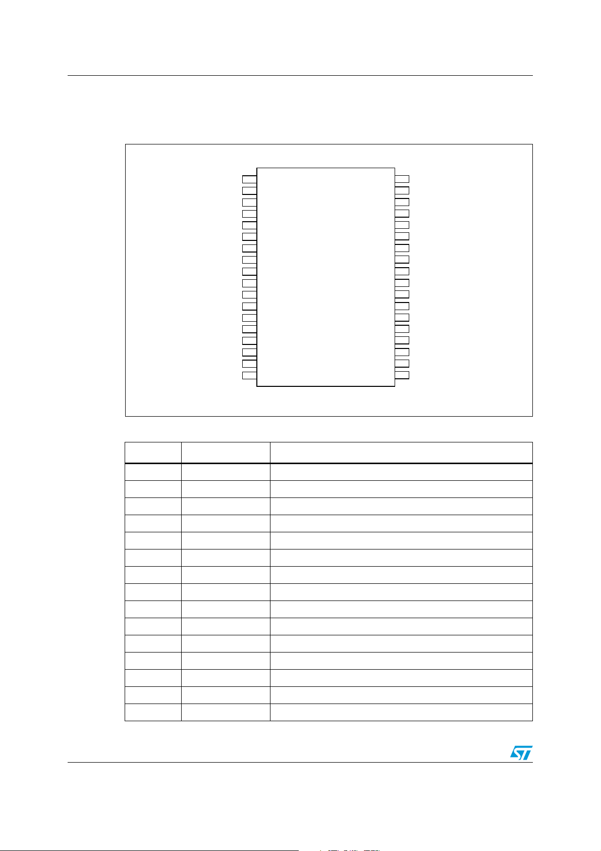
1 Pins configuration
Figure 1. Pins connection (top view)
GND
VBAT
VBAT_SW
BOOST
RES_S
GND_S
VBAT_S
IGN
IGN_ON
PSU_EN
VSD
VSC
VSB
VSA
TRACK_REF
REF_SEL
VS_DIS
REXT
Table 2. Pins description
1
2
3
4
5
6
7
8
9
10
11
12
13
14
15
16
17
18
36
35
34
33
32
31
30
29
28
27
26
25
24
23
22
21
20
19
Pin # Name Description
SW
FDBK
VB
VDD5
VDDL_DRV
VDDL_FDBK
VCORE_FDBK
VCORE_DRV
VPROG3
CORE_DIS
VPROG1
VPROG2
VKAM
VSTBY
STBY_OK
RST5
RSTL
RST_TIM
1 GND Power ground
2 VBAT Battery power source
3 VBAT_SW Switched battery power source
4 BOOST External boost transistor predriver output
5 RES_S Boost (+) current comparator input
6 GND_S Boost (-) current comparator input
7 VBAT_S Battery feedback for boost controller
8 IGN Ignition switch
9 IGN_ON Ignition state
10 PSU_EN Power supply enable
11 VSD Tracking regulator D
12 VSC Tracking regulator C
13 VSB Tracking regulator B
14 VSA Tracking regulator A
15 TRACK_REF Tracking A voltage reference
6/29 Doc ID 14273 Rev 3
L9758 Pins configuration
Table 2. Pins description (continued)
Pin # Name Description
16 REF_SEL Tracking A voltage reference selection
17 VS_DIS Sensor supply disable
18 REXT External current reference resistance
19 RST_TIM Reset timer adjustment
20 RSTL VDDL regulator reset output
21 RST5 VDD5 regulator reset output
22 STBY_OK Standby regulator monitor
23 VSTBY Standby regulator output
24 VKAM Standby memory regulator output
25 VPROG2 Standby regulator voltage selection (VSTBY)
26 VPROG1 Standby memory regulator voltage selection (VKAM)
27 CORE_DIS VDDL and VCORE disable
28 VPROG3 VDDL voltage selection
29 VCORE_DRV VCORE external pass transistor predriver output
30 VCORE_FDBK VCORE feedback
31 VDDL_FDBK VDDL feedback
32 VDDL_DRV VDDL external pass transistor predriver output
33 VDD5 VDD5 linear regulator output
34 VB Switching preregulator output
35 FDBK Switching voltage feedback
36 SW Buck regulator switch output
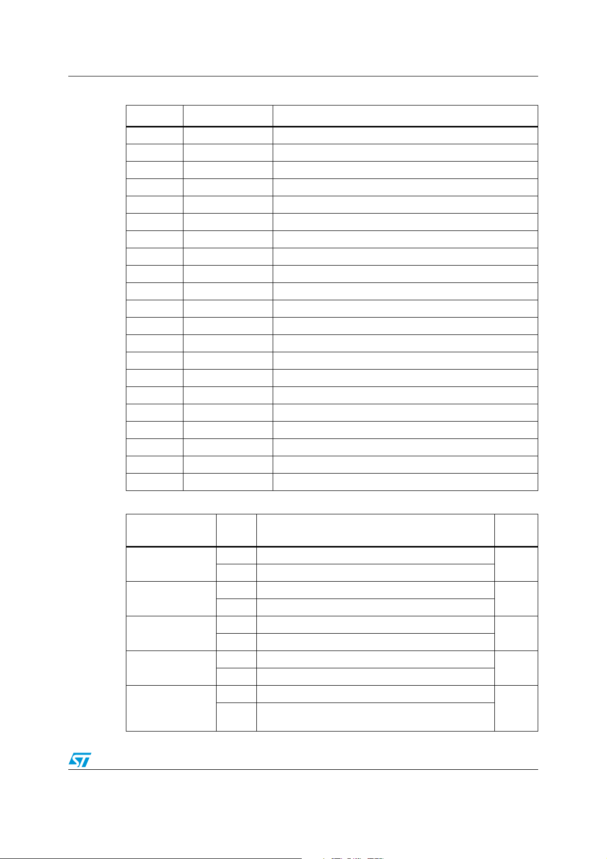
Table 3. Control pins description
Pin name
Logic
level
Description
Low Enter in Stand-by Mode if also PSU_EN is low
IGN
High Enter in Run Mode
Low IGN is high
IGN_ON
High IGN is low
Low Enter in Stand-by Mode if also IGN is low
PSU_EN
High Enter in Run Mode
Low Enable VSB, VSC, VSD tracking regulators
VS_DIS
High Disable VSB, VSC, VSD tracking regulators
Low Voltage reference for VSA tracking regulator is VDD5
Ref_Sel
High
Voltage reference for VSA tracking regulator is
VTRACK_REF
Type of
I/O
Pull
down
Open
drain
Pull
down
Pull
down
Pull
down
Doc ID 14273 Rev 3 7/29
Pins configuration L9758
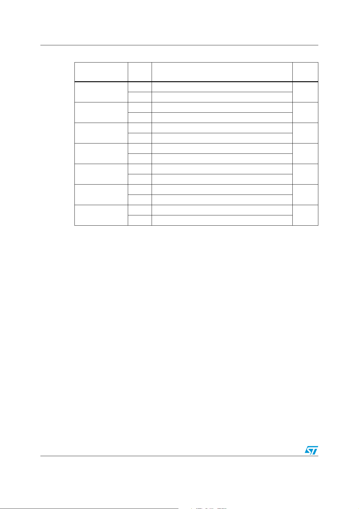
Table 3. Control pins description (continued)
Pin name
RSTL
RST5
VPROG1
VPROG2
VPROG3
CORE_DIS
STBY_OK
Logic
level
Low VDDL output regulator out of range (under voltage)
High VDDL output regulator fully operational
Low VDD5 output regulator out of range (under voltage)
High VDD5 output regulator fully operational
Low VKAM regulator output programmed to 1V
High VKAM regulator output programmed to 1.5V
Low VSTBY regulator output programmed to 2.6V
High VSTBY regulator output programmed to 3.3V
Low VDLL regulator output programmed to 2.6V
High VDLL regulator output programmed to 3.3V
Low Enable VDLL and VCORE linear regulators
High Disable VDLL and VCORE linear regulators
Low VSTBY output regulator out of range (under voltage)
High VSTBY output regulator fully operational
Description
Type of
I/O
Open
collector
Open
collector
Pull up
Pull up
Pull up
Pull
down
Open
drain
8/29 Doc ID 14273 Rev 3
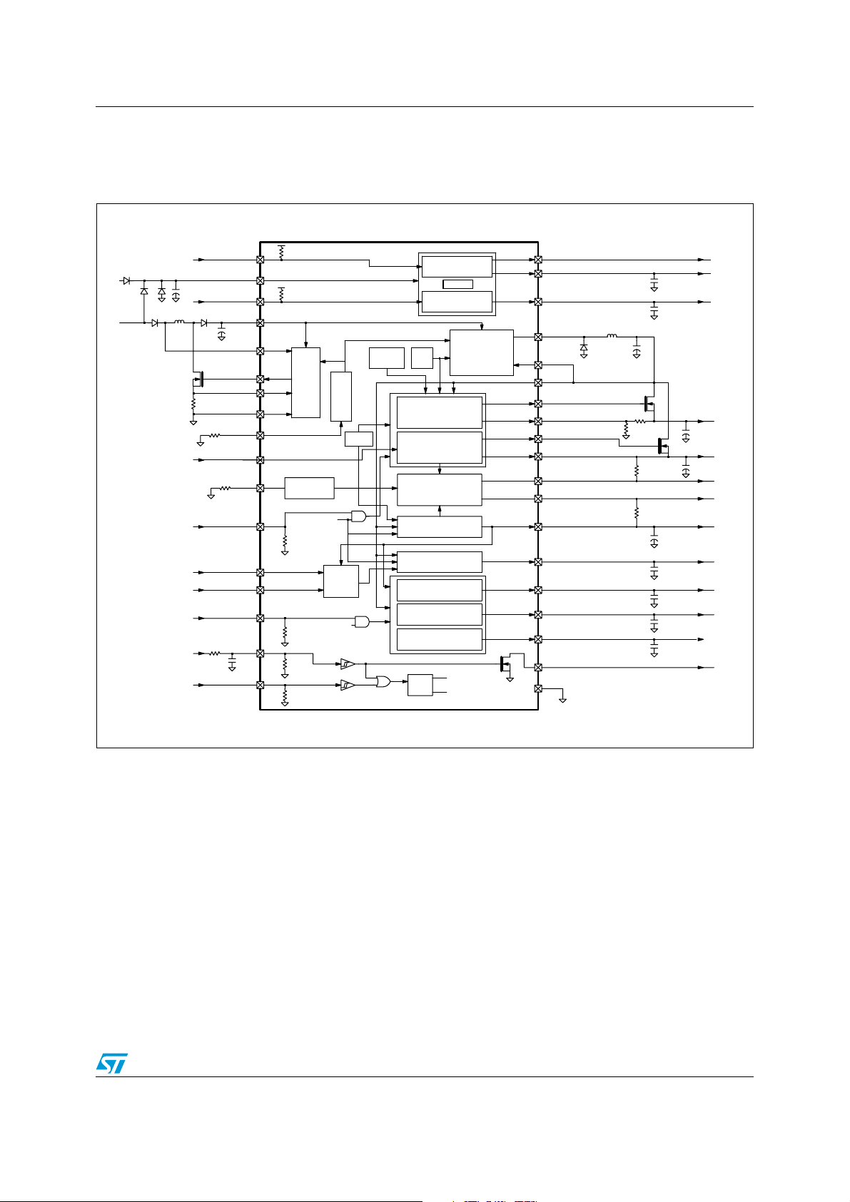
L9758 Functional block diagram
2 Functional block diagram
Figure 2. Functional block diagram
VBAT
STBY
VBAT
RUN
22 µH
10 µF
0.1
TRACK_REF
VPROG2
VBAT
VPROG1
VBAT_SW
300µF
VBAT_S
BOOST
RES_S
GND_S
REXT
10K
VPROG3
RST_TIM
Rtim
CORE_DIS
REF_SEL
VS_DIS
51K
IGN
100 nF
PSU_EN
Boost
Oscillator
/ Divider
EN_REG
Control
Analog
MUX
EN_REG
Charge
Pump
(5 MHz)
SMPS Osc.
SOFT
START
STBY Vreg
2.6V/3.3V, 10mA
Bandgap
VKAM Vreg
1V/1.5V, 10mA
1.5V, 1.0A
5V, 1.0A
50mA
50mA
50mA
50mA
Switchmode
VCORE
VDDL
VDD5
VSA
VSB
VSC
VSD
EN_REG
SOFT START
Band
Gap
Ref.
Linear Voltage Controller
Linear Voltage Controller
2.5V / 3.5V, 1.0A
RESET Logic
VDDL Undervoltage
VDD5 Undervoltage
Power On Reset
Linear Voltage Regulator
Tracking Regulator
Tracking Regulator
Tracking Regulator
Tracking Regulator
Power
Up/Dn
Buck
Power
Supply
Open Drain
STBY_OK
VSTBY
VKAM
SW
FDBK
VB
VCORE_DRV
VCORE_FDBK
VDDL_DRV
VDDL_FDBK
RSTL
RST5
VDD5
VSA
VSB
VSC
VSD
IGN_ON
GND
22 µH
22 µF
2.4K
5.1K
1 µF
1 µF
VCORE_FDBK
22 uF
VDDL
22 uF
10µF
2.2µF
2.2µF
2.2µF
2.2µF
Doc ID 14273 Rev 3 9/29
 Loading...