

Page 1
Octal self configuring low/high side driver
Features
■ Eight independently self configuring low/high
drivers
■ Supply voltage from 4.5 V to 5.5 V
■ R
ON(max)
R
ON(max)
■ Minimum current limit of each output 1 A
■ Output voltage clamping min. 40 V in low-side
configuration
■
Output voltage clamping max. -14 V in high-side
configuration
■ SPI interface for outputs control and for
diagnosis data communication
■ Additional PWM inputs for 3 outputs
■ Independent thermal shutdown for all outputs
open load, short to GND, short to Vb,
overcurrent diagnostics in latched or unlatched
mode for each channel
■ Internal charge pump without need of external
capacitor
■ Controlled SR for reduced EMC
= 0.7 Ω @ Tj = 25 °C,
= 1.2 Ω @Tj = 125 °C
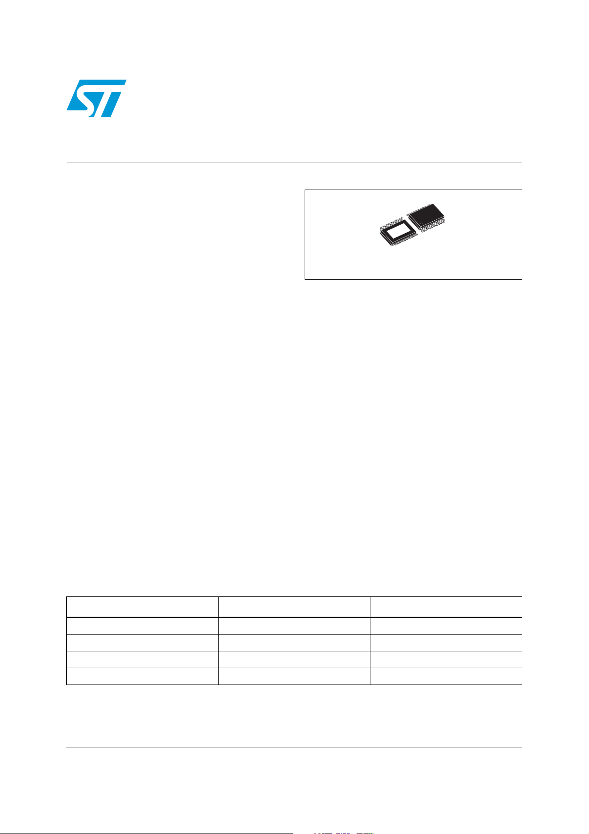
L9733
PowerSSO-28
Outputs 1-8 are self-configuring as high or lowside drives. Self-configuration allows a user to
connect a high or low-side load to any of these
outputs and the L9733 will drive them correctly as
well as provide proper fault mode operation with
no
other needed inputs. In addition, outputs 6, 7 and
8 can be PWM controlled via a external pins (IN6-8).
This device is capable of switching variable load
currents over the ambient range of -40 °C to
+125 °C. The outputs are MOSFET drivers to
minimize Vdd current requirements. For low-side
configured outputs an internal zener clamp from
the drain to gate with a breakdown of 50 V
minimum will provide fast turn off of inductive
loads. When a high-side configured output is
commanded Off after having been commanded
On, the source voltage will go to (VGND - 15 V).
Description
The L9733 is a highly flexible monolithic, medium
current, output driver that incorporates 8 outputs
that can be used as either internal low or high-side
drives in any combination.
Table 1. Device summary
Order code Package Packing
L9733XP PowerSSO-28 (Exposed pad) Tube
L9733XPTR PowerSSO-28 (Exposed pad) Tape and reel
L9733CN PowerSSO-28 (Exposed pad) Tube
L9733CNTR PowerSSO-28 (Exposed pad) Tape and reel
July 2010 Doc ID 11319 Rev 10 1/34
An 16 bit SPI input is used to command the 8
output drivers either "On" or "Off", reducing the
I/O port requirement of the microcontroller.
Multiple L9733 can be daisy-chained. In addition
the SPI output indicates latched fault conditions
that may have occurred.
www.st.com
1
Page 2

Contents L9733
Contents
1 Pin description . . . . . . . . . . . . . . . . . . . . . . . . . . . . . . . . . . . . . . . . . . . . . 6
2 Operating conditions . . . . . . . . . . . . . . . . . . . . . . . . . . . . . . . . . . . . . . . . 8
2.1 Operating range . . . . . . . . . . . . . . . . . . . . . . . . . . . . . . . . . . . . . . . . . . . . . 8
2.1.1 Functional operative range . . . . . . . . . . . . . . . . . . . . . . . . . . . . . . . . . . . 8
2.1.2 Jump start conditions . . . . . . . . . . . . . . . . . . . . . . . . . . . . . . . . . . . . . . . . 8
2.1.3 Operation at low battery condition . . . . . . . . . . . . . . . . . . . . . . . . . . . . . . 9
2.1.4 Operation at load dump condition . . . . . . . . . . . . . . . . . . . . . . . . . . . . . . 9
2.1.5 Loss of protection against short to battery . . . . . . . . . . . . . . . . . . . . . . . . 9
2.2 Absolute maximum ratings . . . . . . . . . . . . . . . . . . . . . . . . . . . . . . . . . . . . . 9
2.3 Thermal data . . . . . . . . . . . . . . . . . . . . . . . . . . . . . . . . . . . . . . . . . . . . . . 10
3 Electrical performance characteristics . . . . . . . . . . . . . . . . . . . . . . . . . 11
3.1 DC characteristics . . . . . . . . . . . . . . . . . . . . . . . . . . . . . . . . . . . . . . . . . . 11
3.2 AC characteristics . . . . . . . . . . . . . . . . . . . . . . . . . . . . . . . . . . . . . . . . . . 14
3.3 SPI characteristics and timings . . . . . . . . . . . . . . . . . . . . . . . . . . . . . . . . 16
4 Functional description . . . . . . . . . . . . . . . . . . . . . . . . . . . . . . . . . . . . . . 18
4.1 Configurations for outputs 1-8 . . . . . . . . . . . . . . . . . . . . . . . . . . . . . . . . . 18
4.1.1 Low-side drivers . . . . . . . . . . . . . . . . . . . . . . . . . . . . . . . . . . . . . . . . . . . 18
4.1.2 High-side drivers . . . . . . . . . . . . . . . . . . . . . . . . . . . . . . . . . . . . . . . . . . 18
4.2 Outputs 1-5 . . . . . . . . . . . . . . . . . . . . . . . . . . . . . . . . . . . . . . . . . . . . . . . 18
4.3 Outputs 6-8 . . . . . . . . . . . . . . . . . . . . . . . . . . . . . . . . . . . . . . . . . . . . . . . 19
4.4 Drn1-8 susceptibility to negative voltage transients . . . . . . . . . . . . . . . . . 19
4.5 Supply pins . . . . . . . . . . . . . . . . . . . . . . . . . . . . . . . . . . . . . . . . . . . . . . . . 19
4.5.1 Main power input (Vdd) . . . . . . . . . . . . . . . . . . . . . . . . . . . . . . . . . . . . . 19
4.5.2 Battery supply (Vbat) . . . . . . . . . . . . . . . . . . . . . . . . . . . . . . . . . . . . . . . 19
4.5.3 Discrete inputs voltage supply (VDO) . . . . . . . . . . . . . . . . . . . . . . . . . . 19
4.6 Discrete inputs . . . . . . . . . . . . . . . . . . . . . . . . . . . . . . . . . . . . . . . . . . . . . 20
4.6.1 Output 6-8 enable input (In6, ln7, ln8) . . . . . . . . . . . . . . . . . . . . . . . . . . 20
4.6.2 Reset input (RES) . . . . . . . . . . . . . . . . . . . . . . . . . . . . . . . . . . . . . . . . . 20
5 Serial peripheral interface (SPI) . . . . . . . . . . . . . . . . . . . . . . . . . . . . . . . 21
2/34 Doc ID 11319 Rev 10
Page 3

L9733 Contents
5.1 Serial data output (DO) . . . . . . . . . . . . . . . . . . . . . . . . . . . . . . . . . . . . . . 21
5.2 Serial data input (DI) . . . . . . . . . . . . . . . . . . . . . . . . . . . . . . . . . . . . . . . . 21
5.3 Chip select (CS) . . . . . . . . . . . . . . . . . . . . . . . . . . . . . . . . . . . . . . . . . . . . 21
5.4 Serial clock (SCLK) . . . . . . . . . . . . . . . . . . . . . . . . . . . . . . . . . . . . . . . . . 22
5.5 Initial input command register and fault register SPI cycle . . . . . . . . . . . . 22
5.6 Input command register . . . . . . . . . . . . . . . . . . . . . . . . . . . . . . . . . . . . . . 22
6 Other L9733 features . . . . . . . . . . . . . . . . . . . . . . . . . . . . . . . . . . . . . . . . 24
6.1 Charge pump usage . . . . . . . . . . . . . . . . . . . . . . . . . . . . . . . . . . . . . . . . . 24
6.2 Waveshaping . . . . . . . . . . . . . . . . . . . . . . . . . . . . . . . . . . . . . . . . . . . . . . 24
6.3 POR register initialization . . . . . . . . . . . . . . . . . . . . . . . . . . . . . . . . . . . . . 24
6.4 Thermal shutdown . . . . . . . . . . . . . . . . . . . . . . . . . . . . . . . . . . . . . . . . . . 24
7 Fault operation . . . . . . . . . . . . . . . . . . . . . . . . . . . . . . . . . . . . . . . . . . . . 25
7.1 Low-side configured output fault operation . . . . . . . . . . . . . . . . . . . . . . . . 25
7.1.1 No latch mode . . . . . . . . . . . . . . . . . . . . . . . . . . . . . . . . . . . . . . . . . . . . 25
7.1.2 Latch mode . . . . . . . . . . . . . . . . . . . . . . . . . . . . . . . . . . . . . . . . . . . . . . 26
7.2 High-side configured output fault operation . . . . . . . . . . . . . . . . . . . . . . . 27
7.2.1 No latch mode . . . . . . . . . . . . . . . . . . . . . . . . . . . . . . . . . . . . . . . . . . . . 27
7.2.2 Latch mode . . . . . . . . . . . . . . . . . . . . . . . . . . . . . . . . . . . . . . . . . . . . . . 28
8 Application circuit . . . . . . . . . . . . . . . . . . . . . . . . . . . . . . . . . . . . . . . . . . 31
9 Package information . . . . . . . . . . . . . . . . . . . . . . . . . . . . . . . . . . . . . . . . 32
10 Revision history . . . . . . . . . . . . . . . . . . . . . . . . . . . . . . . . . . . . . . . . . . . 33
Doc ID 11319 Rev 10 3/34
Page 4

List of tables L9733
List of tables
Table 1. Device summary . . . . . . . . . . . . . . . . . . . . . . . . . . . . . . . . . . . . . . . . . . . . . . . . . . . . . . . . . . 1
Table 2. Pin description . . . . . . . . . . . . . . . . . . . . . . . . . . . . . . . . . . . . . . . . . . . . . . . . . . . . . . . . . . . 6
Table 3. Operating range . . . . . . . . . . . . . . . . . . . . . . . . . . . . . . . . . . . . . . . . . . . . . . . . . . . . . . . . . . 8
Table 4. Absolute maximum ratings . . . . . . . . . . . . . . . . . . . . . . . . . . . . . . . . . . . . . . . . . . . . . . . . . . 9
Table 5. Thermal data. . . . . . . . . . . . . . . . . . . . . . . . . . . . . . . . . . . . . . . . . . . . . . . . . . . . . . . . . . . . 10
Table 6. DC characteristics. . . . . . . . . . . . . . . . . . . . . . . . . . . . . . . . . . . . . . . . . . . . . . . . . . . . . . . . 11
Table 7. AC characteristics . . . . . . . . . . . . . . . . . . . . . . . . . . . . . . . . . . . . . . . . . . . . . . . . . . . . . . . . 14
Table 8. SPI characteristics and timings. . . . . . . . . . . . . . . . . . . . . . . . . . . . . . . . . . . . . . . . . . . . . . 16
Table 9. Bit command register definition . . . . . . . . . . . . . . . . . . . . . . . . . . . . . . . . . . . . . . . . . . . . . 22
Table 10. Command register logic definition . . . . . . . . . . . . . . . . . . . . . . . . . . . . . . . . . . . . . . . . . . . 23
Table 11. Fault register definition . . . . . . . . . . . . . . . . . . . . . . . . . . . . . . . . . . . . . . . . . . . . . . . . . . . . 25
Table 12. Fault logic definition . . . . . . . . . . . . . . . . . . . . . . . . . . . . . . . . . . . . . . . . . . . . . . . . . . . . . . 25
Table 13. Document revision history . . . . . . . . . . . . . . . . . . . . . . . . . . . . . . . . . . . . . . . . . . . . . . . . . 33
4/34 Doc ID 11319 Rev 10
Page 5

L9733 List of figures
List of figures
Figure 1. Pin connection (top view) . . . . . . . . . . . . . . . . . . . . . . . . . . . . . . . . . . . . . . . . . . . . . . . . . . . 6
Figure 2. Output turn on/off delays and slew rates . . . . . . . . . . . . . . . . . . . . . . . . . . . . . . . . . . . . . . 15
Figure 3. DO loading for disable time measurement . . . . . . . . . . . . . . . . . . . . . . . . . . . . . . . . . . . . . 17
Figure 4. Output loading for slew rate measurements . . . . . . . . . . . . . . . . . . . . . . . . . . . . . . . . . . . . 17
Figure 5. SPI input/output timings . . . . . . . . . . . . . . . . . . . . . . . . . . . . . . . . . . . . . . . . . . . . . . . . . . . 17
Figure 6. SPI timing diagram . . . . . . . . . . . . . . . . . . . . . . . . . . . . . . . . . . . . . . . . . . . . . . . . . . . . . . . 17
Figure 7. L9733 application schematic . . . . . . . . . . . . . . . . . . . . . . . . . . . . . . . . . . . . . . . . . . . . . . . 29
Figure 8. L9733 HVAC applicative examples . . . . . . . . . . . . . . . . . . . . . . . . . . . . . . . . . . . . . . . . . . 29
Figure 9. L9733 powertrain applicative examples . . . . . . . . . . . . . . . . . . . . . . . . . . . . . . . . . . . . . . . 30
Figure 10. Optimized circuit layout to achieve proper EMI/ESD capability . . . . . . . . . . . . . . . . . . . . . 31
Figure 11. PowerSSO28 mechanical data and package dimensions . . . . . . . . . . . . . . . . . . . . . . . . . 32
Doc ID 11319 Rev 10 5/34
Page 6
Pin description L9733
1 Pin description
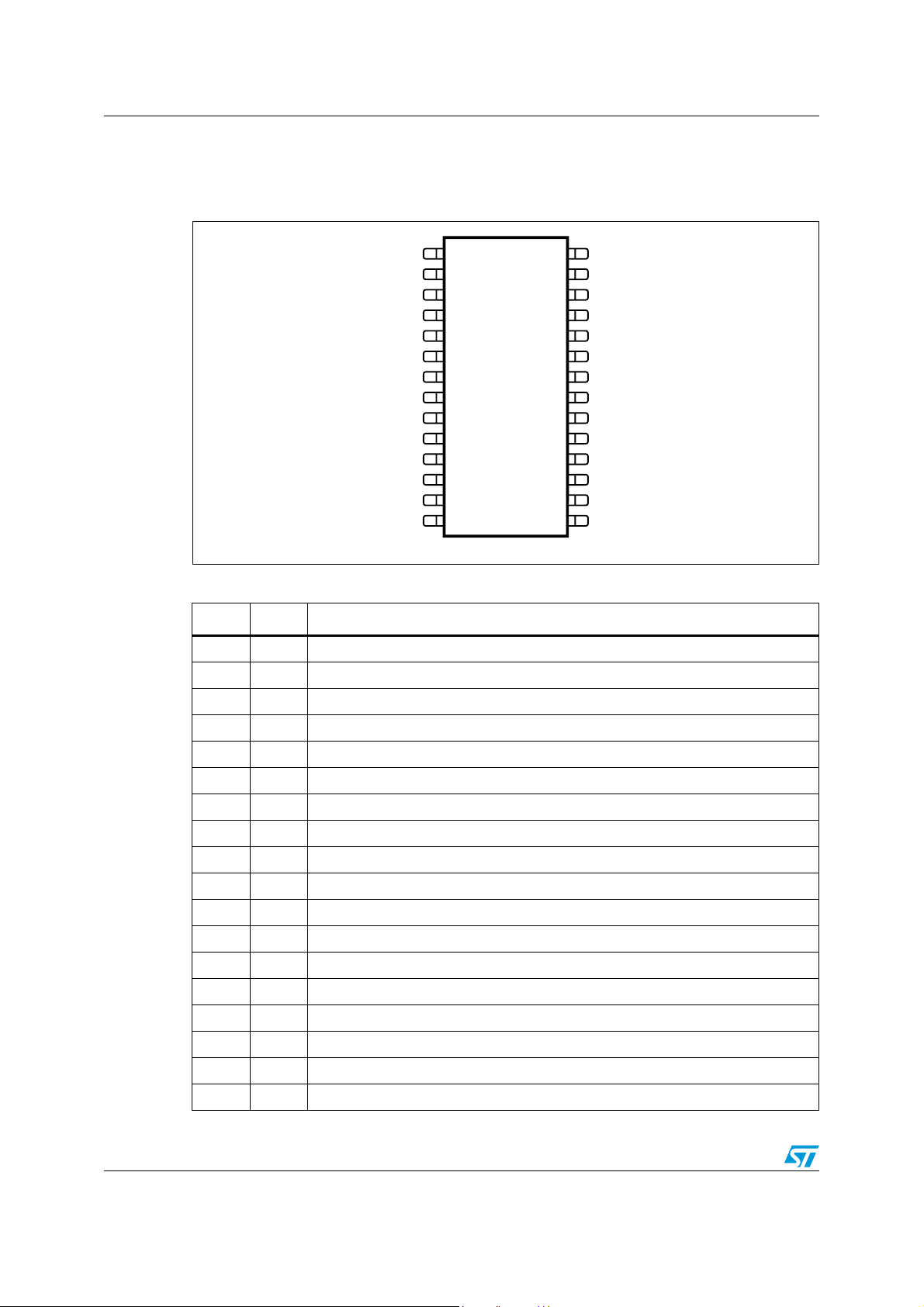
Figure 1. Pin connection (top view)
SCLK
SRC1
DRN1
DRN2
SRC2
SRC3
DRN3 DRN6
DRN4 DRN5
SRC4
Table 2. Pin description
VDD
2
CS
IN6
IN7 IN8
3
4
5
6
7
8
9
10
12
13
D06AT544
28
27
26
25
24
23
22
21
20
19
18
17
16
1514Vbat GND
N° Pin Function
1 VDD 5 Volt supply input
2 SCLK SPI serial clock input
3 CS SPI chip select (active low)
4 SRC1 Source pin of configurable driver #1 (0.7 Ω Rds
5 DRN1 Drain pin of configurable driver #1(0.7 Ω Rds
6 DRN2 Drain pin of configurable driver #2 (0.7 Ω Rds
7 SRC2 Source pin of configurable driver #2 (0.7 Ω Rds
8 SRC3 Source pin of configurable driver #3 (0.7 Ω Rds
9 DRN3 Drain pin of configurable driver #3 (0.7 Ω Rds
10 DRN4 Drain pin of configurable driver #4 (0.7 Ω Rds
11 SRC4 Source pin of configurable driver #4 (0.7 Ω Rds
12 IN6 Discrete input used to PWM output driver #6
13 IN7 Discrete input used to PWM output driver #7
VDO1
D0
D1
SRC8
DRN8
DRN7
SRC7
SRC6
SRC511
RES
@ +25 °C)
on
@ +25 °C)
on
@ +25 °C)
on
@ +25 °C)
on
@ +25 °C)
on
@ +25 °C)
on
@ +25 °C)
on
@ +25 °C)
on
14 Vbat Battery supply voltage
15 GND Analog ground
16 IN8 Discrete input used to PWM output driver #8
17 RES Reset input (active low)
18 SRC5 Source pin of configurable driver #5 (0.7 Ω Rds
6/34 Doc ID 11319 Rev 10
@ +25 °C)
on
Page 7
L9733 Pin description
Table 2. Pin description (continued)
N° Pin Function
19 DRN5 Drain pin of configurable driver #5 (0.7 Ω Rdson @ +25 °C)
20 DRN6 Drain pin of configurable driver #6 (0.7 Ω Rds
21 SRC6 Source pin of configurable driver #6 (0.7 Ω Rds
22 SRC7 Source pin of configurable driver #7 (0.7 Ω Rds
23 DRN7 Drain pin of low-side driver #7 (0.7 Ω Rds
24 DRN8 Drain pin of low-side driver #8 (0.7 Ω Rds
25 SRC8 Source pin of configurable driver #8 (0.7 Ω Rds
@ +25 °C)
on
on
on
@ +25 °C)
on
@ +25 °C)
on
on
@ +25 °C)
@ +25 °C)
@ +25 °C)
26 DI SPI data in
27 DO SPI data out
28 VDO Microcontroller logic interface voltage
Note: The exposed slug must be soldered on the PCB and connected to GND.
Doc ID 11319 Rev 10 7/34
Page 8
Operating conditions L9733
2 Operating conditions
2.1 Operating range
This part may not operate if taken outside the operating range. Once the condition is
returned to within the specified maximum rating or the power is recycled, the part will
recover with no damage or degradation.
Table 3. Operating range
Symbol Parameter Value Unit
V
dd
V
(operative
bat
range)
@ JSC 18 to 27
V
bat
V
@ low
bat
battery
V
@ load
bat
dump
T
j
I
Ox
Eso Maximum clamping energy at switch-off 20 mJ
Supply voltage 4.5 to 5.5 V
Battery supply voltage
Thermal junction temperature range -40 to 150 °C
Snubbing voltage of DRN1-8 min 50 VDC
Output current 1-8 max 800 mA
2.1.1 Functional operative range
4.5 V ≤ V
All the electrical capabilities are guaranteed by characterization as reported in Section 3:
Electrical performance characteristics.
2.1.2 Jump start conditions
≤ 18 V (-40 °C ≤ Tj ≤ 150 °C);
bat
4.5V to 18
V
3.5 to 4.5
27 to 40
18 V ≤ V
≤ 27 V (-40 °C ≤ Tj ≤ 150 °C);
bat
Operation at Jump start condition for a maximum duration of 1 minute.
All ouputs are switched according to the commands on the SPI bus or the PWM inputs. The
SPI bus and the inputs are functional during the Jump-Start condition.
The over-temperature shutdown and over current protection of the device is not guaranteed
to stay functional for Vbat between 18 V and 27 V.
The reliability and the functionality of the L9733XP are not compromised when the JumpStart condition is not repeated for more than five times.
8/34 Doc ID 11319 Rev 10
Page 9
L9733 Operating conditions
2.1.3 Operation at low battery condition
3.5 V ≤ V
≤ 4.5 V (-40 °C ≤ Tj ≤ 150 °C);
bat
All outputs are able to keep the status in according to the commands on the SPI bus or the
PWM inputs. Switching commands entered via the SPI bus might not be executed by the
L9733 at low-battery condition. The SPI bus and the inputs are functional during the LowBattery condition.
2.1.4 Operation at load dump condition
27 V ≤ V
There is not an internal circuit that switches OFF the drivers during load dump condition.
The over-temperature shutdown and over current protection of the device is not guaranteed
to stay functional during load dump condition.
≤ 40 V (-40 °C ≤ Tj ≤ 150 °C)
bat
2.1.5 Loss of protection against short to battery
When the battery supply voltage, V
bat (pin 14)
condition at a output in high-side configuration, the protection circuits are no longer
functional, and the L9733 may fail with EOS.
is switched off during a short-to-battery
2.2 Absolute maximum ratings
This part may be irreparably damaged if taken outside the specified absolute maximum
ratings. Operation outside the absolute maximum ratings may also cause a decrease in
reliability.
Table 4. Absolute maximum ratings
Symbol Parameter Value Unit
V
V
I
I
ESD
1. For the DRNx the MAX ASB value is the Max Clamp Voltage (see Table 6 on page 13 - DRNx Clamp
voltage).
2. Device is only protected vs. GND.
Supply voltage -0.3 to 7 V
DD
Supply voltage -0.3 to 40 V
bat
CS,DI,DO,SCLK,EN,IN6,IN7,IN8,VDO -0.3 to 7.0 V
SRCx pin min. -24 VDC
Max. value of V
DRN1-8
Current limit of output 1-8 (-40 °C) 2.5 A
OL
Over current protection at output 1-8 (-40 °C) 3 A
OP
Maximum clamping energy 20 mj
Human body model - All pins ±2
Human body model - Driver outputs ±4
(1)
= Minimum of {V
SRCx
Doc ID 11319 Rev 10 9/34
+1V ||| V
bat
+0,3 V ||| +40 V}
DRNx
-0.3 to 60 VDC
(2)
(2)
kV
kV
Page 10
Operating conditions L9733
2.3 Thermal data
Table 5. Thermal data
Symbol Parameter Min Typ Max Unit
T
T
R
R
th-hys
R
Th j-amb
R
Th j-case
1. With 2s2p PCB thermally enhanced.
Operating ambient temperature -40 - 125 °C
amb
Storage temperature -50 - 150 °C
stg
T
Maximum operating junction temperature - - 150 °C
j
Thermal shutdown temperature 151 175 200 °C
th
Thermal shutdown temperature hysteresis 7 10 25 °C
Thermal resistance junction-to-ambient
Thermal resistance junction-to-case - - 3 °C/W
(1)
--24°C/W
10/34 Doc ID 11319 Rev 10
Page 11
L9733 Electrical performance characteristics
3 Electrical performance characteristics
These are the electrical capabilities this part was designed to meet. It is required that every
part meet these characteristics.
3.1 DC characteristics
T
= -40 to 125 °C, Vdd = 4.5 to 5.5 Vdc, V
amb
unless otherwise specified.
Table 6. DC characteristics
Symbol Parameter Conditions Min Typ Max Units
= 4.5 to 18 Vdc (high-side configuration),
bat
IN6v
IN6v
I
IN6il
I
IN6ih
IN7v
IN7v
I
IN7il
I
IN7ih
IN8v
IN8v
I
IN8il
I
IN8ih
CS
CS
I
CSih
I
CSil
SCLK
SCLK
I
SCLKih
I
SCLKil
DI
DI
I
DIih
I
DIil
DO
DO
ih
IN6 input voltage
il
- - 0.7vdo V
0.3vdo - - V
In6 = 0 VDC - - |10| μA
IN6 input current
In6 = VDO 10 - 100 μA
ih
IN7 input voltage
il
- - 0.7vdo V
0.3vdo - - V
In7 = 0 VDC - - |10| μA
IN7 input current
In7 = VDO 10 - 100 μA
ih
IN8 input voltage
il
- - 0.7vdo V
0.3vdo - - V
In8 = 0 VDC - - |10| μA
IN8 input current
In8 = VDO 10 - 100 μA
ih
CS input voltage
il
- - 0.7vdo V
0.3vdo - - V
CS = VDO - - |10| μA
CS input current
CS = 0 VDC 10 - 100 μA
ih
SCLK input voltage
il
- - 0.7vdo V
0.3vdo - - V
SCLK = VDO - - |10| μA
SCLK input current
SCLK = 0 VDC 10 - 100 μA
ih
il
DI input voltage
- - 0.7vdo V
0.3vdo - - V
DI = VDO - - |10| μA
DI input current
DI = 0 VDC 10 - 100 μA
= 2.5 mA - - 0.4 V
ol
oh
DO output voltages
I
DO
IDO = -2.5 mA vdo-0.6 - - V
Doc ID 11319 Rev 10 11/34
Page 12

Electrical performance characteristics L9733
Table 6. DC characteristics (continued)
Symbol Parameter Conditions Min Typ Max Units
I
DOzol
I
DOzoh
RES
ih
RES
il
I
RESil
I
RESih
POR
th
I
slp
I
vbat
I
VDD
I
VDD
I
DRN1lk
I
DRN8lk
I
SRC1lk
I
SRC8lk.
I
Drn1-8sink
R
DRN1-8
I
Drn1-8source
I
src1-8sink
I
src1-8source
V
Drn1-8open
DO Tri-state currents
DO = 0 VDC - - |10| μA
DO = VDO - - |10| μA
- - 0.7vdo V
RES input voltage
0.3vdo - - V
RES = 0 VDC 10 - 100 μA
RES input current
RES = VDO - - |10| μA
@ -40 °C 2.8 - 4.2
Power on reset threshold
@ 125 °C 2 - 3.4
VDD = SRC1-8 = 0VDC
Vbat sleep current
Vbat current
DRN1-DRN8=18VDC, Vb. Sum
currents (T
@ -40 °C)
(T
amb
amb
> 0 °C)
VDD = 5 V
All Outputs Commanded On
--
--15mA
Max. VDD current All Outputs Commanded On - - 8.5 mA
Min. VDD current All Outputs Commanded Off 0.5 - mA
DRN1 - DRN8
leakage currents
(low-side)
SRC1 – SRC8
Leakage currents
(high-side)
DRN1 – DRN8 sink current
(low-side)
Open load detection
resistance
VDD = 0 VDC: SRC1-8 = 0 VDC
DRN1- DRN8 = 16 VDC
--510μA
DRN1- DRN8 = 40 VDC
VDD = 0 VDC: SRC1-8 = 0 VDC
DRN1- 8 = 16 V
---5
DRN1- 8 = 40 VDC
SRC1-8 = GND DI = AC00h
R
load
R
load
≤ 11 kΩ
≤ 200 kΩ
10
120
-100
VBAT>=9V 11 - 200 KΩ
Source current DRN1-DRN8 = GND -10 - -100 μA
SRC1 – SRC8
sink/source current
(high-side)
DRN1- 8 = Vb, DI = AC00h
SCR1- 8 = Vb 10
-
SCR1- 8 = GND -18 - -100 μA
SRC1- 8 = GND, DI = AC00h
DRN1 – DRN8
DRN1- DRN8 = Open
VDD=4.9 to 5.1 VDC
2.7 - 3.1 V
open load voltage
(low-side)
SRC1- 8 = GND, DI = AC00h
DRN1- DRN8 = Open
2.5 - 3.5 V
VDD = 4.5 to 5.5 V
V@ 25 °C 2.8 - 3.7
10
3
μA
μA
μA
μA
-10
μA
μA
280
μA
100 μA
12/34 Doc ID 11319 Rev 10
Page 13

L9733 Electrical performance characteristics
Table 6. DC characteristics (continued)
Symbol Parameter Conditions Min Typ Max Units
V
src1-8open
I
DRN1limit
I
DRN8limit
I
DRN1OVC
I
DRN8OVC
I
SRC1limit
I
SRC8limit
I
SRC1OVC
I
SRC8OVC
DRN1
DRN8Cl+
SRC1
SRC8Cl+
V
Drn1-8open
- DRN18
VthGND
DRN1-
8
VthVbat
V
Drn1-8open
V
Drn1-8open
- SRC18
VthGND
SRC1 – SRC8 open load
voltage (High-side)
DRN1 - DRN8
DRN1 - DRN8
current limits
(low-side)
DRN1 - DRN8
overcurrent threshold
(low-side)
SRC1 – SRC8
current limits
(high-side)
Overcurrent threshold
(high-side)
DRN1 - DRN8
-
Cl+
Clamp voltages (low-side)
SRC1 – SRC8
-
Cl+
Clamp voltages (High-side)
Short to GND threshold
distance from open load
voltage (low-side)
DRN1 - DRN8
Short to Vbat threshold
distance from open load
voltage (low-side)
SRC1 - SRC8
Short to GND threshold
distance from open load
voltage (High-side)
DRN1-8 = Vb, DI = AC00h
SCR1-8 = open
DI = ACFFh, DI = AAFFh
SRC1 – SRC8 = 0 VDC
DRN1 - DRN8 = 4.5 - 16 VDC
> 0 °C)
(T
amb
(T
@ -40 °C)
amb
DI = AC00h, DI = AA00h SRC1 –
SRC8 = 0 VDC
DRN1 - DRN8 = 4.5 - 16 VDC
> 0 °C)
(T
amb
- 40 °C)
(T
amb
DI = ACFFh, DI = AAFFh
DRN1 - DRN8 = Vb
SRC1 – SRC8 = GND
> 0 °C)
(T
amb
- 40 °C)
(T
amb
DRN1 - DRN8 = Vbat
SRC1 – SRC8 = GND
> 0 °C)
(T
amb
- 40 °C)
(T
amb
DI = AC00h
SRC1-8 = GND, I
DRN1-8
= 350 mA
DI = AC00h
DRN1-8 = Vbat, I
SRC1-8
= -350 mA
SRC1 – SRC8 = GND:
Decrease Drn1 - Drn8 until Faults
are ”Set”
DI = AC00h
SRC1 – SRC8 = GND: Increase
Drn1 - Drn8 until Faults are ”Not
Set”
DI = AC00h
Drn1 – Drn8 = Vb: Decrease SRC1
- SRC8 until Faults are ”Not Set”
2.0 - 2.8 V
1
1
2.2
2.5
1
1
2.7
3
1
1
1
1
2.2
2.5
-
2.7
3
50 - 60 V
-24 - -14 V
0.3 - 0.7 V
0.3 - 0.7 V
0.2 - 0.6 V
A
A
A
A
A
A
A
A
SRC1-
8
VthVbat
V
Drn1-8open
SRC1 – SRC8
Short to Vbat threshold
distance from open load
voltage (High-side)
DI = AC00h
Drn1 – Drn8 = Vbat: Increase
SCR1 - SCR8 until Faults are ”
0.2 - 0.6 V
Set”
Doc ID 11319 Rev 10 13/34
Page 14

Electrical performance characteristics L9733
Table 6. DC characteristics (continued)
Symbol Parameter Conditions Min Typ Max Units
Rdson
Drn1-8
Drn1-8
ther
On resistance
(1)
(Drn to SRC1-8)
Thermal shutdown
(2)
temperature
@ +125 °C @ I
@ +25 °C @ IDRN = 350 mA - - 0.7 Ω
@ -40 °C @ I
DI = ACFFh, I
SRC1 – SRC8 = GND, Increase
temperature until Drn1 - Drn8 > 2
= 350 mA - - 1.2 Ω
DRN
= 350 mA - 0.5 Ω
DRN
= 1 mA,
Drn1-8
151 - 200 °C
VDC, Verify DO Bits 0-15 are ”Set”
(2)
Drn1-8
hyst
1. R
dsonDrn1-8
2. Design Information, not tested.
Hysteresis Drn1 - Drn8 < 2 VDC 5 - 15 °C
≤ 1.2 Ω; at V
between 3.5 V and 27 V and T between -40 °C and 150 °C
bat
3.2 AC characteristics
T
= -40 to 125 °C, Vdd = 4.5 to 5.5 Vdc, V
amb
Table 7. AC characteristics
Symbol Parameter Conditions Min Typ Max Units
DRN1 - DRN8
T
filtDRN1-8
Open load & short to
GND filter time (low-side)
DI = AC00h, DI = A3FFh
SRC1 – SRC8 = GND
(Latch mode)
= 4.5 to 18 Vdc, unless otherwise specified
bat
300 - 900 μs
T
filtSRC1-8
T
delDRN1-8
T
delSRC1-8
T
res
Drn1-8
Drn1-8
SRC1 - SRC8
Open load & short to
Vbat filter time
(high-side)
DI = AC00h, DI = A3FFh
DRN1 – DRN8 = Vb
300 - 900 μs
(Latch mode)
DRN1 - DRN8
Overcurrent switch off
delay
DI = ACFFh, DI = AA00h
SRC1 – SRC8 = GND
10 - 75 μs
(low-side)
SRC1 - SRC8
Overcurrent switch off
delay
DI = ACFFh, DI = AA00h
DRN1 – DRN8 = Vb
10 - 75 μs
(high-side)
Restart time after
overcurrent switch off
DI = ACFFh, DI = AA00h 120 - 450 ms
time (Int)
Slew rate
htol
turn on
Turn off (low-side) 0.5 - 1.5 V/μs
ltoh
Outputs loaded as Figure 4
See Figure 2
See Figure 2
0.65
-
1.95 V/μs
14/34 Doc ID 11319 Rev 10
Page 15

L9733 Electrical performance characteristics
Table 7. AC characteristics (continued)
Symbol Parameter Conditions Min Typ Max Units
SRC1-8
SRC1-8
Drn1-8
Drn1-8
SRC1-8
SRC1-8
Drn1-8
SRC1-8
Slew rate
htol
turn on
Turn off (High-side) 0.5 - 1.5 V/μs
ltoh
Delay time
tondly
Tur n o n
Turn off (low-side) 10 - 100 μs
toffdly
Delay time
tondly
Tur n o n
Turn off (high-side) 10 - 100 μs
toffdly
Delay delta Drn1-8
offon
Delay delta SRC1-8
offon
Outputs loaded as Figure 4
See Figure 2
See Figure 2
Outputs loaded as Figure 4
See Figure 2
See Figure 2
Outputs loaded as Figure 4
See Figure 2
See Figure 2
- Drn1-8
toffdly
- SRC1-8
toffdly
Figure 2. Output turn on/off delays and slew rates
6- 8IN6- 8
IN
90%
90%
20%
20%
80%
10% 10%
LSD
HSD
DRN1-8
DRN1-8htol
DRN1-8htol
DRN1-8tondly
SRC1-8
SRC1-8
SRC1-8ltoh
SRC1-8tondly
SRC1-8tondly
tondly
tondly
0.65
2
2
10 - 60 μs
10 - 60 μs
6-8
IN
DRN1-8
DRN1-8ltoh
DRN1-8ltoh
DRN1-8toffdlyDRN1-8toffdly
SRC1-8
SRC1-8
SRC1-8htol
SRC1-8toffdly
SRC1-8toffdly
-
20%
20%
90%
90%
80%
-
-
-
1.95 V/μs
20 μs
20 μs
IN1- 5 are available on wafer only
IN1- 5 are available on wafer only
Doc ID 11319 Rev 10 15/34
Page 16

Electrical performance characteristics L9733
3.3 SPI characteristics and timings
T
= -40 to 125 °C, Vdd = 4.5 to 5.5 Vdc, V
amb
Table 8. SPI characteristics and timings
Symbol Parameter Conditions Min Typ Max Units
= 4.5 to 18 Vdc, unless otherwise specified
bat
DINC
in
SCLK
DO
DO
DO
DO
DO
DO
tth
rise
fall
a
sum
hm
dis
Filt
Input capacitance
Cin
Output data (do)
rise time
Output data (do)
fall time
50 pF from DO to Ground
See Figure 5
See Figure 5 - - 70 ns
Access time See Figure 6 --350ns
Set up time See Figure 6 20 - - ns
Hold time See Figure 6 10 - - ns
Output data (DO)
disable time
No Capacitor on DO, See Figure 5 --400ns
Filter time All Fault bits are “Set” 5 - 20 μs
SCLKwid SCLK width See Figure 5, @ f
SCLKlm SCLK low time See Figure 5, @ f
SCLKhm SCLK high time See Figure 5, @ f
SCLKrise SCLK rise time See Figure 5, @ f
SCLKfall SCLK fall time See Figure 5, @ f
CSrise
Channel select (CS)
rise time
See Figure 5
(1)
SCLK
SCLK
SCLK
SCLK
SCLK
= 5.4MHz
= 5.4MHz
= 5.4MHz
= 5.4MHz
= 5.4MHz
- - 20 pF
- - 20 pF
- - 70 ns
(1)
185 - - ns
(1)
58 - - ns
(1)
58 - - ns
(1)
- - 21 ns
(1)
- - 21 ns
--100ns
CSfall
CSlead
CSlag
DIrise
DIfall
DIsus
DIhs
Channel select (CS)
fall time
Channel select (CS)
lead time
Channel select (CS)
lag time
Input data (DI)
rise time
Input data (DI)
fall time
Input data (DI)
set-up time
Input data (DI)
hold time
See Figure 5
Figure 6
See
See
Figure 6
See Figure 5, @ f
See Figure 5 @ f
See Figure 6, @ f
See Figure 6, @ f
CS2SCLK CS rise to SCLK rise See Figure 6, @ f
1. Guaranteed by design.
(1)
(1)
(1)
SCLK
SCLK
SCLK
SCLK
SCLK
= 5.4MHz
= 5.4MHz
= 5.4MHz
= 5.4MHz
= 5.4MHz
16/34 Doc ID 11319 Rev 10
--100ns
455 - - ns
50 - - ns
(1)
- - 30 ns
(1)
- - 30 ns
(1)
15 - - ns
(1)
10 - - ns
(1)
40 - 300 ns
Page 17

L9733 Electrical performance characteristics
Figure 3. DO loading for disable time measurement
+5 V
1 k
1 k
1 k
1 k
+5 V
4.0 V
4.0 V
DO
DOdis
CS
CS
DOdis
1.0 V
1.0 V
Ω
Ω
0 V
0 V
Ω
Ω
DO
DO
DO
Vcc
Vcc
Figure 4. Output loading for slew rate measurements
Vbat
Outputs 1-8
All Low Side Outputs must
meet the slew rate requirements
of this load condition
Figure 5. SPI input/output timings
90%
90%
10%
10%
90% 90%
90% 90%
CS
10%
10%
CS
DOrise
DOrise
10%
10%
Figure 6. SPI timing diagram
CS
CS
meet the slew rate requirements
180
Ω
SCLKwid
SCLKwid
SCLKlm SCLKhm
SCLKlm SCLKhm
SCLKrise
SCLKrise
CSfallCSrise
CSfallCSrise
90%
90%
DO
DO
SCLK
SCLK
10%
10%
All High Side Outputs must
of this load condition
Outputs 1-8
180
CLKfall
CLKfall
S
S
DI
DI
DOfall
DOfall
Ω
DIfallDIrise
DIfallDIrise
CS
CS
lead
lead
SCLK
SCLK
DO
DO
a
a
DO
DO
sum
DO
DO
FAULT LSB FAULT MSB
FAULT LSB FAULT MSB
DI
DI
sum
DI LSB DI MSB
DI LSB DI MSB
DI
DI
sus
sus
DI
DI
hs
hs
Doc ID 11319 Rev 10 17/34
DO
DO
CS
CS
lag
lag
CS2SCLK
hm
hm
DI
DI
CS2SCLK
DO
DO
dis
dis
Page 18

Functional description L9733
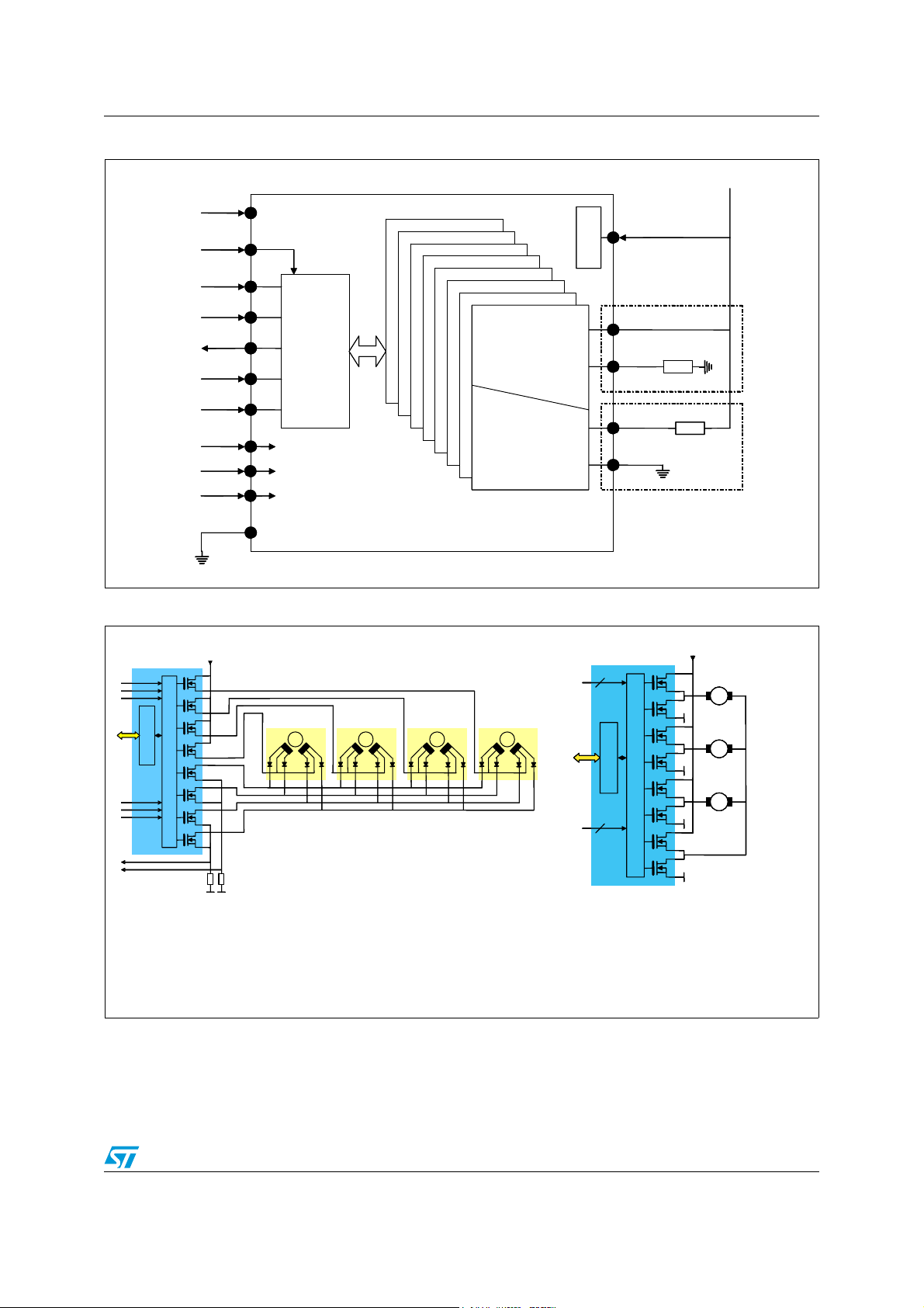
4 Functional description
L9733 integrates 8 self-configuring outputs (OUT1-8) which are able to drive either
incandescent lamps, inductive loads (non-pwm'd, in pwm is necessary an external diode to
reduce flyback power dissipation), or resistive loads biased to Vbat (low-side configuration)
or to GND (high-side configuration). These outputs can be enabled and disabled via the SPI
bus. Each of these outputs has a short circuit protection (with 0.8-2.4 Amps threshold)
selectable via SPI bus between a filtered switching OFF overcurrent protection or a linear
current limitation (default condition after power ON is switching OFF protection enabled).
An over-temperature protection as described in Section 2.1 is available for each outputs.
When a high-side configured output is commanded OFF after having been commanded ON,
the source voltage will go to (VGND - 15 V). This is due to the design of the circuitry and the
transconductance of the MOSFET. When a low-side configured output is commanded OFF
after having been commanded ON, the output voltage will rise to the internal zener clamp
voltage (50 VDC minimum) due to the flyback of the inductive load.
Outputs 1-8 are able to drive any combination of inductive loads or lamps at one time.
Inductive loads for the L9733 can range from 35mH to a maximum of 325 mH. The
recommended worst-case solenoid loads (at -40 °C) are calculated using a minimum
resistance of 40Ω for each output. The maximum single pulse inductive load energy the
L9733 outputs is able to be safely handle is 20 mJ at -40 °C to 125 °C (Worst-case load of
325 mH and 40 Ω).
4.1 Configurations for outputs 1-8
The drain and source pins for each output must be connected in one of the two following
configurations (see Figure 7).
4.1.1 Low-side drivers
When any combination of outputs 1-8 are connected in a low-side drive configuration the
source of the applicable output (Src1-8) shall be connected to ground. The drain of the
applicable output (Drn1-8) shall be connected to the low-side of the load.
4.1.2 High-side drivers
When any combination of outputs 1-8 are connected in a high-side drive configuration the
Drain of the applicable output (Drn1-8) shall be connected to Vbat. The source of the
applicable output (Src1-8) shall be connected to the high-side of the load.
4.2 Outputs 1-5
These five outputs can be used as either high or low-side drives. The room temperature
Rdson of these outputs is 0.7 Ω. A current limited (100 µA max) voltage generator is
connected to Src 1-5 for open load and short to GND detection when a low-side configured
output is commanded OFF. Another current limited (100 µA max if VDrn 1-5 > 60 %Vbat,
280 µA max if VDrn 1-5 < 60 % Vbat) voltage generator is connected to Drn 1-5 for open
load and short to V bat detection when a high-side configured output is commanded OFF.
Drain pins of outputs 1-5 (Drn1-5) are connected to the drains of the N channel MOSFET
18/34 Doc ID 11319 Rev 10
Page 19

L9733 Functional description
transistors. Source pins of outputs 1-5 (Src1-5) are connected to the sources of the
N-channel MOSFET transistors.
4.3 Outputs 6-8
These three self-configuring outputs can be used to drive either high or low-side loads. In
addition to being controlled by the SPI BUS these outputs can also be enabled and disabled
via the IN6 & IN7& IN8 inputs. The IN6, IN7 and IN8 inputs are logically or'd with the SPI
commands to allow either the IN6 & IN7 & IN8 inputs or the SPI commands to activate these
outputs. The use of the IN6 & IN7 & IN8 pins for PWM control on these outputs should only
be done with non-inductive loads if an external flyback diode is not present. The room
temperature Rdson of these four outputs is 0.7 Ω. A current limited (100µA max) voltage
generator is connected to Src 6-8 for open load and short to GND detection when a low-side
configured output is commanded OFF. Another current limited (100µA max if VDrn 6-8 >
60%Vbat, 280 µA max if VDrn 6-8 < 60 %Vbat) voltage generator is connected to Drn 6-8
for open load and short to Vbat detection when a high-side configured output is commanded
OFF.
Drain pins of Outputs 6-8 (Drn6-8) are connected to the drains of the N channel MOSFET
transistors. Source pins of Outputs 6-8 (Src6-8) are connected to the sources of the N
channel MOSFET transistors.
4.4 Drn1-8 susceptibility to negative voltage transients
All outputs connected in the low-side configuration must have a ceramic chip capacitor of
0.01µF to 0.1 µF connected from drain to ground. This is needed to prevent potential
problems with the device operation due to the presence of fast negative transient(s) on the
drain(s) of the device. Adequate de-coupling capacitors from the Drain (VBAT) to ground
shall be provided for high-side configured outputs.
4.5 Supply pins
4.5.1 Main power input (Vdd)
An external +5.0 ±0.5 VDC supply provided from an external source is the primary power
source to the L9733. This supply is used as the power source for all of its internal logic
circuitry and other miscellaneous functions.
4.5.2 Battery supply (Vbat)
This input is the supply for the on board charge pump. This input shall be connected directly
to battery. If this input is not connected to the same supply, without additional voltage drops,
of the drains of any high-side connected outputs, then the Rdson of that given output will be
higher than the specified maximum.
4.5.3 Discrete inputs voltage supply (VDO)
This pin is used to supply the discrete input stages of L9733 and must be connected to the
same voltage used to supply the peripherals of the processor interfaced to L9733.
Doc ID 11319 Rev 10 19/34
Page 20

Functional description L9733
4.6 Discrete inputs
4.6.1 Output 6-8 enable input (In6, ln7, ln8)
This input allows Output 6 (or Output 7, or Output 8) to be enabled via this external pin
without the use of the SPI. The SPI command and the In6-7 input are logically or'd together.
A logic "1" on this input (In6, ln7 or ln8) will enable this output no matter what the status of
the SPI command register. A logic "0" on this input will disable this output if the SPI
command register is not commanding this output on. This pins (In6, ln7 or ln8) can be left
"open" if the internal output device is being controlled only via the SPI. This input has a
nominal 100kΩ resistor connected from this pin to ground, which will pull this pin to ground if
an open circuit condition occur. This input is ideally suited for non-inductive loads that are
pulse width modulated (PWM'd). This allows PWM control without the use of the SPI inputs.
4.6.2 Reset input (RES)
When this input goes low it resets all the internal registers and switches off all the output
stages. This input has a nominal 100 kΩ resistor connected from this pin to VDD, which will
pull this pin to VDD if an open circuit condition occur.
20/34 Doc ID 11319 Rev 10
Page 21

L9733 Serial peripheral interface (SPI)
5 Serial peripheral interface (SPI)
The L9733 has a serial peripheral interface consisting of Serial Clock (SCLK), Data Out
(DO), Data In (DI), and Chip Select (CS). All outputs will be controlled via the SPI. The input
pins CS, SCLK, and DI, thanks to VDO pin, have level input voltages allowing proper
operation from microcontrollers that are using 5.0 or 3.3 volts for their Vdd supply. The
design of the L9733 allows a "daisy-chaining" of multiple L9733's to further reduce the need
for controller pins.
5.1 Serial data output (DO)
This output pin is in a tri-state condition when CS is a logic '1'. When CS is a logic '0', this
pin transmits 16 bits of data from the fault register to the digital controller. After the first 16
bits of DO fault data are transmitted (after a CS transition from a logic '1' to a logic '0'), then
the DO output sequentially transmits the digital data that was just received (16 SCLK cycles
earlier) on the DI pin. The DO output continues to transmit the 16 SCLK delayed bit data
from the DI input until CS eventually transitions from a logic '0' to a logic '1'. DO data
changes state 10 nsec or later, after the falling edge of SCLK. The LSB is the first bit of the
byte transmitted on DO and the MSB is the last bit of the byte transmitted on DO, once CS
transitions from a logic '1' to a logic '0'.
5.2 Serial data input (DI)
This input takes data from the digital controller while CS is low. The L9733 accepts an 16 bit
byte to command the outputs on or off. The L9733 also serially wraps around the DI input
bits to the DO output after the DO output transmits its 16 fault flag bits. The LSB is the first
bit of each byte received on DI and the MSB is the last bit of each byte received on DI, once
CS transitions from a logic '1' to a logic '0'. The last 4 bits (b15-b12) of the first 16 bit byte
are used as key-word. The 4 bits (b11-b8) of the first 16 bits byte are used to select writing
mode between OUT8-1 status and diagnosis operating mode . The DI input has a nominal
100 kΩ resistor connected from this pin to the VDO pin, which pulls this pin to VDO if an
open circuit condition occurs.
5.3 Chip select (CS)
This is the chip select input pin. On the falling edge of CS, the DO pin is released from tristate mode. While CS is low, register data are shifted in and shifted out the DI pin and DO
pin, respectively, on each subsequent SCLK. On the rising edge of CS, the DO pin is tristated and the fault register is "Cleared" if a valid DI byte has been received. A valid DI byte
is defined as such:
– a multiple of 16 bits was received.
– a valid key-word was received
The fault data is not cleared unless all of the 2 previous conditions have been met. The CS
input has a nominal 100 kΩ resistor connected from this pin to the VDO pin, which pulls this
pin to VDO if an open circuit condition occurs.
Doc ID 11319 Rev 10 21/34
Page 22

Serial peripheral interface (SPI) L9733
5.4 Serial clock (SCLK)
This is the clock signal input for synchronization of serial data transfer. DI data is shifted into
the DI input on the rising edge of SCLK and DO data changes on the falling edge of SCLK.
The SCLK input has a nominal 100kΩ resistor connected from this pin to the VDO pin,
which pulls this pin to VDO if an open circuit condition occurs.
5.5 Initial input command register and fault register SPI cycle
After initial application of Vdd to the L9733, the input command register and the fault register
are "Cleared" by the POR circuitry and that means that the default condition for the output
status is Off, the default diagnostic mode is No Latch and the switching OFF overcurrent
protection is enable. During the initial SPI cycle, and all subsequent cycles, valid fault data
will be clocked out of DO (fault bits).
5.6 Input command register
An input byte (16 bits) is routed to the Command Register. The content of this Command
Register is given in table 9. Additional DI data will continue to be wrapped around to the DO
pin. If CS should happen to go high before complete reception of the current byte, this just
transmitted byte shall be ignored (invalid).
Table 9. Bit command register definition
Key word Writing mode: output Output status
MSB LSB
1 0 1 0 1 1 0 0 OUT 8 OUT 7 OUT 6 OUT 5 OUT 4 OUT 3 OUT 2 OUT 1
b15 b14 b13 b12 b11 b10 b9 b8 b7 b6 b5 b4 b3 b2 b1 b0
Key word Writing mode: diag Driver diag mode
MSB LSB
1 0 1 0 0 0 1 1 Diag 8 Diag 7 Diag 6 Diag 5 Diag 4 Diag 3 Diag 2 Diag 1
b15 b14 b13 b12 b11 b10 b9 b8 b7 b6 b5 b4 b3 b2 b1 b0
Key word Writing mode: protect Driver overcurrent protection
MSB LSB
1 0 1 0 1 0 1 0 Ilim 8 Ilim 7 Ilim 6 Ilim 5 Ilim 4 Ilim 3 Ilim 2 Ilim 1
b15 b14 b13 b12 b11 b10 b9 b8 b7 b6 b5 b4 b3 b2 b1 b0
22/34 Doc ID 11319 Rev 10
Page 23

L9733 Serial peripheral interface (SPI)
Table 10. Command register logic definition
Bit State Status Writing mode
b0-b7 0 OUT1 - OUT8 are commanded off Output
b0-b7 1 OUT1 - OUT8 are commanded on Output
b0-b7 0 OUT1 - OUT8 diagnostic is No Latch Mode Diag
b0-b7 1 OUT1 - OUT8 diagnostic is Latch Mode Diag
b0-b7 0 OUT1 - OUT8 switching OFF overcurrent protection Protection
b0-b7 1 OUT1 - OUT8 linear overcurrent protection Protection
Doc ID 11319 Rev 10 23/34
Page 24

Other L9733 features L9733
6 Other L9733 features
6.1 Charge pump usage
In order to provide low Rdson values when connected in a high-side configuration, a charge
pump to drive the internal gate voltage(s) above Vbat is implemented. The charge pump
used on the L9733 doesn't need external capacitor. The L9733 uses a common charge
pump and oscillator for all the 8 configurable output channels. The charge pump uses the
Vbat supply connected directly to the Vb pin. The normal range of the Vbat voltage is 10 to
18V18V. However, the L9733 is functional with Vbat voltages as low as 4.5V DC with
eventually a degradation of Rdson.
The frequency range of this charge pump is from 3.6 to 7.6 MHz. The frequency is above
1.8 MHz in order to be above the AM radio band and below 8.0 MHz so that harmonics do
not get within the FM radio band.
6.2 Waveshaping
Both the turn on and the turn off slew rates on all outputs (OUT1-8) are limited to between
10 µs and 100 µs for both rise and fall times (10 to 90 %, and vice versa), to reduce
conducted EMC energy in the vehicle's wiring harness. The characteristics of the turn-on
and turn-off voltage is linear, with no discontinuities, during the output driver state transition.
6.3 POR register initialization
When the L9733 wakes up, the Vdd supply to the L9733 is allowed from 0 to 5 VDC in 0.3 to
3ms. The L9733 has a POR circuit, which monitors the Vdd voltage. When the Vdd voltage
reaches an internal threshold, and remains above this trip level for at least 5 to 20 µs, the
Command and Fault registers are "cleared". Before Vdd reaches this trip level, none of the
eight outputs are allowed to momentarily glitch on.
6.4 Thermal shutdown
Each of the eight outputs has independent thermal protection circuitry that disables each
output driver once the local N-Channel MOSFET's device temperature reaches between
+151 and +200 °C. A filter is present to validate the thermal fault (5 µs to 20 µs). There is a
5 to 15 °C hysteresis between the enable and disable temperature levels. The faulted
channel will periodically turn off and on until the fault condition is cleared, the ambient
temperature is decreased sufficiently or the output is commanded off. If a thermal shutdown,
of one or more output drivers, is active during the falling edge of the chip select (CS) signal
all the bits of the Fault Register are "setted" to "1" (thermal shutdown is not latched and
could be read only in the moment it is present). The thermal fault is cleared on the rising
edge of Chip Select if a valid DI byte was received.
Note: Due to the design of the L9733 each output's thermal limit "may not" be truly independent to
the extent that if one output is shorted, it may impact the operation of other outputs (due to
lateral heating in the die).
24/34 Doc ID 11319 Rev 10
Page 25

L9733 Fault operation
7 Fault operation
The fault diagnostic capability consists of one internal 16 bits shift register and 2 bits are
used for each output. The diagnostic information are: no fault present, overcurrent, open
load and short circuit.
For L9733XP all of the faults will be cleared on the rising edge of chip select if a valid DI byte
was received.
For L9733CN The OVC register will be cleared after the end of the diagnosis restart time
Tr
or by the input signal (IN) in low state. The other faults will be cleared on the rising edge
es
of chip select if a valid DI byte was received.
Table 11. Fault register definition
OUT 8 OUT 7 OUT6 OUT5 OUT4 OUT3 OUT2 OUT1
MSB LSB
D1 D0 D1 D0 D1 D0 D1 D0 D1 D0 D1 D0 D1 D0 D1 D0
b15 b14 b13 b12 b11 b10 b9 b8 b7 b6 b5 b4 b3 b2 b1 b0
Table 12. Fault logic definition
D1 D0 Fault status
0 0 No fault is present
0 1 Open load
1 0 Short circuit to GND (low-side) or short circuit to Vbat (high-side)
1 1 Overcurrent
If all the bits b0-b15 of the fault register have value '1' it means that a thermal fault, at least
on one of the eight independent Outputs, occurred.
7.1 Low-side configured output fault operation
The diagnostic circuitry verifies for the low-side configured output the following condition:
Normal operation, open load, short circuit to GND and overcurrent (only if the switching OFF
protection, selectable for each channel via SPI bus, is active).
The diagnostic circuitry operates in two different modes, selected for each channel by SPI:
no latch mode and latch mode. The fault priority is overcurrent and then open load or short
circuit to GND, this means that if an overcurrent occurs the fault register is always
overwritten and following open load or short to GND faults that happen before that the
register is cleared will be ignored.
7.1.1 No latch mode
This diagnostic operating mode doesn't latch open load and short to GND faults.
1. Open load
The diagnostic of open load is detected only in OFF condition sensing the Drn1-8
output voltage. This fault is detected on the falling edge of the CS input if the power
Doc ID 11319 Rev 10 25/34
Page 26

Fault operation L9733
drain voltage is inside the voltage range limited by the two thresholds Vth_Vbat and
Vth_GND. An internal current limited voltage regulator fixes the drain voltage inside the
described range when no load is connected.
2. Short circuit to GND
The diagnostic of short circuit to GND is detected only in OFF condition sensing the
Drn1-8 output voltage. This fault is detected on the falling edge of the CS input if the
power drain voltage is lower than the Vth_GND threshold.
3. Overcurrent
The diagnostic of overcurrent is detected only in ON condition, if the switching OFF
protection of the channel is enabled (default), sensing the current level of the output
power transistor. If the output current has been above the short threshold Iovc for the
filtering time Tdel the output power is switched off and at the same time an overcurrent
fault is written in the fault register.
There are three possibilities to restart one output after the fault has occurred:
– Automatically after a time Tre s
– On the rising edge of CS if two valid DI byte has been received and first the Output
Status in the command register is written with logic '0' and then with a logic “1” in
the following SPI cycle
– On the rising edge (low to high transition) at the corresponding parallel input pin
(only for Outputs 6-8).
– If the switching OFF protection is not active the On phase overcurrent protection is
a linear current limitation and no diagnosis is available.
The use of the IN6-8 pins for PWM control on the outputs 6-8 could generates bad
diagnostic behavior when the falling edge of CS happens a short time after the falling edge
of IN6-8 during the power MOS transient. Software filtering may be needed to ignore fault
signals during Drn6-8 transient after falling edge of IN6-8.
7.1.2 Latch mode
This diagnostic operating mode latches all faults when they happen.
1. Open load
The diagnostic of open load is detected only in OFF condition sensing the Drn1-8
output voltage. This fault is detected if the power drain voltage is inside the voltage
range limited by the two thresholds Vth_Vbat and Vth_GND for the filtering time Tfilt.
An internal current limited voltage regulator fixes the drain voltage inside the described
range when no load is connected.
2. Short circuit to GND
The diagnostic of short circuit to GND is detected only in OFF condition sensing the
Drn1-8 output voltage. This fault is detected if the power drain voltage is lower than the
Vth_GND threshold for the filtering time Tfilt.
3. Overcurrent
The diagnostic of overcurrent is detected only in ON condition, if the switching OFF
protection of the channel is enabled (default), sensing the current level of the output
power transistor. If the output current has been above the short threshold Iovc for the
filtering time Tdel the output power is switched off and at the same time an overcurrent
fault is written in the fault register. If the switching OFF protection is not active the On
26/34 Doc ID 11319 Rev 10
Page 27

L9733 Fault operation
phase overcurrent protection is a linear current limitation and no diagnosis is available.
There are three possibilities to restart one output after the fault has occurred:
– Automatically after a time Tre s
– On the rising edge of CS if two valid DI byte has been received and first the Output
Status in the command register is written with logic '0' and then with a logic “1” in
the following SPI cycle
– On the rising edge (low to high transition) at the corresponding parallel input pin
(only for Outputs 6-8).
If the power MOS transient, after a switching-off command, is longer than Tdel
filtering time, a bad diagnostic behavior happens and software filtering may be
needed.
7.2 High-side configured output fault operation
The diagnostic circuitry verifies for the high-side configured output the following condition:
Normal operation, open load, short circuit to Vbat and overcurrent (only if the switching OFF
protection, selectable for each channel via SPI bus, is active).
The diagnostic circuitry operates in two different modes, selected for each channel by SPI:
no latch mode and latch mode. The fault priority is overcurrent and then open load or short
circuit to Vb, this means that if an overcurrent occurs the fault register is always overwritten
and following open load or short to Vbat faults that happen before that the register is cleared
will be ignored.
7.2.1 No latch mode
This diagnostic operating mode doesn't latch open load and short to Vbat faults.
1. Open load
The diagnostic of open load is detected only in OFF condition sensing the Src1-8
output voltage. This fault is detected on the falling edge of the CS input if the power
drain voltage is inside the voltage range limited by the two thresholds Vth_Vbat and
Vth_GND. An internal current limited voltage regulator fixes the drain voltage inside the
described range when no load is connected.
2. Short Circuit to Vb
The diagnostic of short circuit to Vbat is detected only in OFF condition sensing the
Src1-8 output voltage. This fault is detected on the falling edge of the CS input if the
power drain voltage is higher than the Vth_Vbat threshold.
3. Overcurrent
The diagnostic of overcurrent is detected only in ON condition, if the switching OFF
protection of the channel is enabled (default), sensing the current level of the output
power transistor. If the output current has been above the short threshold Iovc for the
filtering time Tdel the output power is switched off and at the same time an overcurrent
fault is written in the fault register.
There are three possibilities to restart one output after the fault has occurred:
– Automatically after a time Tre s
– On the rising edge of CS if two valid DI byte has been received and first the Output
Status in the command register is written with logic '0' and then with a logic “1” in
the following SPI cycle
Doc ID 11319 Rev 10 27/34
Page 28

Fault operation L9733
– On the rising edge (low to high transition) at the corresponding parallel input pin
(only for Outputs 6-8).
– If the switching OFF protection is not active the On phase overcurrent protection is
a linear current limitation and no diagnosis is available.
The use of the IN6-8 pins for PWM control on the outputs 6-8 could generates bad
diagnostic behavior when the falling edge of CS happens a short time after the
falling edge of IN6-8 during the power MOS transient. Software filtering may be
needed to ignore fault signals during Drn6-8 transient after falling edge of IN6-8.
7.2.2 Latch mode
This diagnostic operating mode latches all faults when they happen.
1. Open load
The diagnostic of open load is detected only in OFF condition sensing the Src1-8
output voltage. This fault is detected if the power drain voltage is inside the voltage
range limited by the two thresholds Vth_Vbat and Vth_GND for the filtering time Tfilt.
An internal current limited voltage regulator fixes the drain voltage inside the described
range when no load is connected.
2. Short Circuit to Vb
The diagnostic of short circuit to Vbat is detected only in OFF condition sensing the
Src1-8 output voltage. This fault is detected if the power drain voltage is higher than the
Vth_Vbat threshold for the filtering time Tfilt.
3. Overcurrent
The diagnostic of overcurrent is detected only in ON condition, if the switching OFF
protection of the channel is enabled (default), sensing the current level of the output
power transistor. If the output current has been above the short threshold Iovc for the
filtering time Tdel the output power is switched off and at the same time an overcurrent
fault is written in the fault register.
There are three possibilities to restart one output after the fault has occurred:
– Automatically after a time Tre s
– On the rising edge of CS if two valid DI byte has been received and first the Output
Status in the command register is written with logic '0' and then with a logic “1” in
the following SPI cycle
– On the rising edge (low to high transition) at the corresponding parallel input pin
(only for Outputs 6-8).
If the switching OFF protection is not active the On phase overcurrent protection is
a linear current limitation and no diagnosis is available.
If the power MOS transient, after a switching-off command, is longer than Tdel filtering time,
a bad diagnostic behavior happens and software filtering may be needed.
28/34 Doc ID 11319 Rev 10
Page 29
L9733 Fault operation
Figure 7. L9733 application schematic
VDD
VDD
RES
RES
SCLK
SCLK
DI
DI
DO
DO
CS
CS
VDO
VDO
IN6
IN6
IN7
IN7
IN8
IN8
GND
GND
SPI Control Logic
SPI Control Logic
To driver 6
To driver 6
To driver 7
To driver 7
To driver 8
To driver 8
Registers
Registers
8 HIGH/LOW SIDE DRIVER
8 HIGH/LOW SIDE DRIVER
High Side Driver
High Side Driver
High Side Driver
Configuration
Configuration
Configuration
Low Side Driver
Low Side Driver
Low Side Driver
Configuration
Configuration
Configuration
CP
CP
VBAT
VBAT
DRN[x]
DRN[x]
SRC[x]
SRC[x]
DRN[x]
DRN[x]
SRC[x]
SRC[x]
BAT
BAT
V
V
Figure 8. L9733 HVAC applicative examples
Vbatt
Vbatt
SPI
SPI
Control Logic
Control Logic
L9733
L9733
Stall sense
Stall sense
Four flap motors become sequentially driven. Unipolar stepper motor are
Four flap motors become sequentially driven. Unipolar stepper motor are
selected by 4 high-side configured switches. If the decoupling diodes are inside
selected by 4 high-side configured switches. If the decoupling diodes are inside
the motor housing, only 8 wires are needed to drive this arrangement.
the motor housing, only 8 wires are needed to drive this arrangement.
SMSMSMSM
SMSMSMSM
4 channels configured to low- and 4 channels
4 channels configured to low- and 4 channels
configured to high side build a quad half bridge.
configured to high side build a quad half bridge.
This can drive 3 DC-motors sequantially.
L9733
L9733
L9733
SPI
SPI
SPI
Vbatt
Vbatt
Vbatt
M
M
M
M
M
M
Contr ol Logi c
Contr ol Logi c
Contr ol Logi c
M
M
M
M
M
M
M
M
M
M
M
M
Doc ID 11319 Rev 10 29/34
Page 30

Fault operation L9733
Figure 9. L9733 powertrain applicative examples
Vbatt
Vbatt
Vbatt
Vbatt
Tach-Out
Tach-Out
(PWM)
(PWM)
Key-On Relay
Key-On Relay
Control Logic
Control Logic
SPI
SPI
Fuel Pump Relay
Fuel Pump Relay
(opt PWM)
L9733
L9733
Main Relays and Lamps Driving
Main Relays and Lamps Driving
(opt PWM)
Coolant Fan Relay
Coolant Fan Relay
Power Latch Relay
Power Latch Relay
Canister Purge Relay
Canister Purge Relay
(opt PWM)
(opt PWM)
MIL Lamp
MIL Lamp
Water Lamp
Water Lamp
Starter Relay
Starter Relay
A/C Fan Relay
A/C Fan Relay
A/C Compressor Relay
A/C Compressor Relay
Control Logic
Control Logic
SPI
SPI
L9733
L9733
Idle speed stepper motor driving and auxiliary loads
Idle speed stepper motor driving and auxiliary loads
Air Pump Relay
Air Pump Relay
SM
SM
Idle Speed Control
Idle Speed Control
30/34 Doc ID 11319 Rev 10
Page 31

L9733 Application circuit
8 Application circuit
Figure 10. Optimized circuit layout to achieve proper EMI/ESD capability
Voltage
Reg.
Positive ISO - pulse
protection
VDD 5V
VDD
RES
SCLK
VDD on/off for low
quiescent current
VDO
Capacitor impedance
IN 6
IN 7
IN 8
Frequency
VBAT supplies the floating charge pump. Filtering
capacitor C1 is important to achieve a proper EMI
performance. Impedance minimum should fit to
the critical frequency range. A series resistor to
VBAT can improve furthermore EMI performance.
47…100nF
Ceramic
DI
DO
CS
R1= 10...22 (EMI improvement)
VBAT
SPI
C1
Control
GND
Reverse polarity & neg. ISO -pulse protection
47…100nF Ceramic
DRNX
All output C = 47nF ceramic
Central ground plane (blue coloured)
Battery
Module
Connector
Doc ID 11319 Rev 10 31/34
Page 32

Package information L9733
9 Package information
In order to meet environmental requirements, ST offers these devices in different grades of
ECOPACK
®
packages, depending on their level of environmental compliance. ECOPACK
®
specifications, grade definitions and product status are available at: www.st.com.
ECOPACK
®
is an ST trademark.
Figure 11. PowerSSO28 mechanical data and package dimensions
DIM.
A 2.15 2.45 0.084 0.0965
A2 2.15 2.35 0.084 0.0925
a1 0 0.10 0 0.004
b 0.18 0.36 0.007 0.014
c 0.23 0.32 0.009 0.012
(1)
D
(1)
E
e0.65 0.025
e3 8.45 0.033
F 2.3 0.090
G 0.10 0.004
G1 0.06 0.002
H 10.10 10.50 0.398 0.413
h 0.40 0.016
k5˚ (typ)
L 0.60 1.0 0.023 0.039
M 4.3 0.169
N 10˚ (max)
O 1.2 0.047
Q 0.8 0.031
S 2.9 0.114
T3.65 0.144
U 1.0 0.039
X 4.2 4.8 0.165 0.189
Y 6.6 7.2 0.259 0.283
(1) "D” and “E" do not include mold flash or protrusions Mold flash
or protrusions shall not exceed 0.15 mm per side(0.006”)
mm inch
MIN. TYP. MAX. MIN. TYP. MAX.
10.10 10.50 0.398 0.413
7.4 7.6 0.291 0.299
OUTLINE AND
MECHANICAL DATA
PowerSSO-28
(Exposed pad)
32/34 Doc ID 11319 Rev 10
7633868 C
Page 33

L9733 Revision history
10 Revision history
Table 13. Document revision history
Date Revision Changes
13-Apr-2005 1 Initial release.
15-Jun-2006 2 Changed only look and feel.
08-Aug-2006 3 Modified Table 9: Bit command register definition on page 22.
28-May-2007 4 Changed the min. value of the CSlead parameter on the Ta bl e 8 .
17-Jul-2007 5
03-Aug-2007 6 Updated in Ta b le 4 the ESD parameter.
12-Jun-2008 7
02-Dec-2008 8
13-May-2009 9
27-Jul-2010 10
Updated Ta bl e 6 and Ta bl e 7 . Added new Figure 4.
Changed the status from Preliminary data to Datasheet.
Added order codes in Table 1: Device summary.
Added “CS2SCLK” parameter in Table 8: SPI characteristics and
timings.
Updated Figure 6: SPI timing diagram.
Updated Table 1: Device summary on page 1.
Removed all references to the SO-28 package.
Updated Section 2.1: Operating range and Section 2.2: Absolute
maximum ratings.
Added Section 2.1.1: Functional operative range, Section 2.1.2:
Jump start conditions, Section 2.1.3: Operation at low battery
condition and Section 2.1.4: Operation at load dump condition.
Added Section 8: Application circuit.
Added “POR
Updated Table 1: Device summary on page 1.
Updated Figure 11: PowerSSO28 mechanical data and package
dimensions.
Updated Table 1: Device summary on page 1.
Updated Section 7: Fault operation on page 25.
” parameter in Table 6: DC characteristics.
th
Doc ID 11319 Rev 10 33/34
Page 34

L9733
Please Read Carefully:
Information in this document is provided solely in connection with ST products. STMicroelectronics NV and its subsidiaries (“ST”) reserve the
right to make changes, corrections, modifications or improvements, to this document, and the products and services described herein at any
time, without notice.
All ST products are sold pursuant to ST’s terms and conditions of sale.
Purchasers are solely responsible for the choice, selection and use of the ST products and services described herein, and ST assumes no
liability whatsoever relating to the choice, selection or use of the ST products and services described herein.
No license, express or implied, by estoppel or otherwise, to any intellectual property rights is granted under this document. If any part of this
document refers to any third party products or services it shall not be deemed a license grant by ST for the use of such third party products
or services, or any intellectual property contained therein or considered as a warranty covering the use in any manner whatsoever of such
third party products or services or any intellectual property contained therein.
UNLESS OTHERWISE SET FORTH IN ST’S TERMS AND CONDITIONS OF SALE ST DISCLAIMS ANY EXPRESS OR IMPLIED
WARRANTY WITH RESPECT TO THE USE AND/OR SALE OF ST PRODUCTS INCLUDING WITHOUT LIMITATION IMPLIED
WARRANTIES OF MERCHANTABILITY, FITNESS FOR A PARTICULAR PURPOSE (AND THEIR EQUIVALENTS UNDER THE LAWS
OF ANY JURISDICTION), OR INFRINGEMENT OF ANY PATENT, COPYRIGHT OR OTHER INTELLECTUAL PROPERTY RIGHT.
UNLESS EXPRESSLY APPROVED IN WRITING BY AN AUTHORIZED ST REPRESENTATIVE, ST PRODUCTS ARE NOT
RECOMMENDED, AUTHORIZED OR WARRANTED FOR USE IN MILITARY, AIR CRAFT, SPACE, LIFE SAVING, OR LIFE SUSTAINING
APPLICATIONS, NOR IN PRODUCTS OR SYSTEMS WHERE FAILURE OR MALFUNCTION MAY RESULT IN PERSONAL INJURY,
DEATH, OR SEVERE PROPERTY OR ENVIRONMENTAL DAMAGE. ST PRODUCTS WHICH ARE NOT SPECIFIED AS "AUTOMOTIVE
GRADE" MAY ONLY BE USED IN AUTOMOTIVE APPLICATIONS AT USER’S OWN RISK.
Resale of ST products with provisions different from the statements and/or technical features set forth in this document shall immediately void
any warranty granted by ST for the ST product or service described herein and shall not create or extend in any manner whatsoever, any
liability of ST.
ST and the ST logo are trademarks or registered trademarks of ST in various countries.
Information in this document supersedes and replaces all information previously supplied.
The ST logo is a registered trademark of STMicroelectronics. All other names are the property of their respective owners.
© 2010 STMicroelectronics - All rights reserved
STMicroelectronics group of companies
Australia - Belgium - Brazil - Canada - China - Czech Republic - Finland - France - Germany - Hong Kong - India - Israel - Italy - Japan -
Malaysia - Malta - Morocco - Philippines - Singapore - Spain - Sweden - Switzerland - United Kingdom - United States of America
www.st.com
34/34 Doc ID 11319 Rev 10
 Loading...