

Page 1
Features
■ High performance clamping at ground and
positive reference voltage
■ Fast active clamping
■ Operating range 4.75 V - 5.25 V
■ Single voltage for supply and positive
reference
■ Low quiescent current
■ Low input leakage current
L9700D-E
Hex precision limiter
'!0'#&4
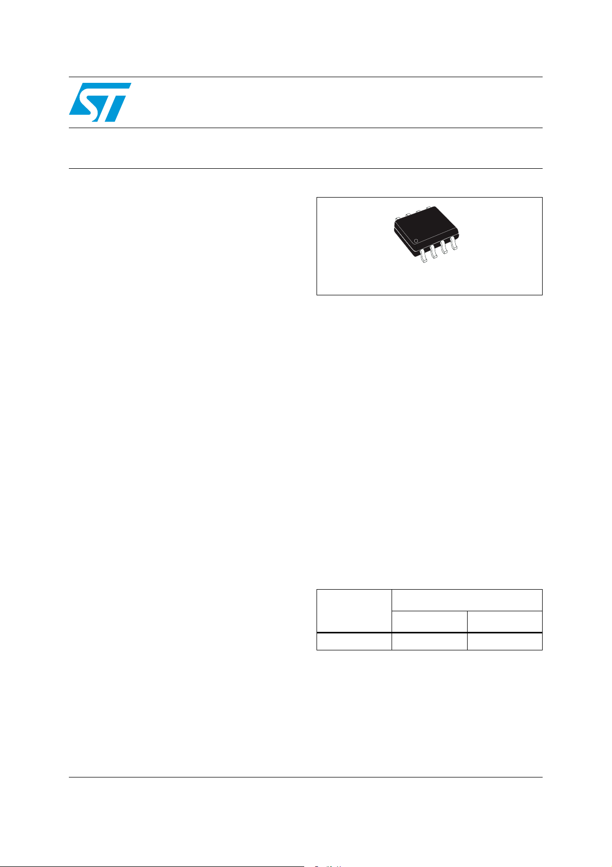
SO-8
Description
The L9700D-E is a monolithic circuit which is
suited for input protection and voltage clamping
purpose.
The limiting function is referred to ground and the
positive supply voltage.
One single element contains six independent
channels.
Very fast speed is achieved by internal feedback
and the application of a new vertical PNPtransistor with isolated collector.
Table 1. Device summary
Order code
Package
Tube Tape and real
SO-8 L9700D-E L9700DTR-E
October 2011 Doc ID 022301 Rev 1 1/14
www.st.com
1
Page 2

Contents L9700D-E
Contents
1 Block diagram and pin connection . . . . . . . . . . . . . . . . . . . . . . . . . . . . . 5
2 Electrical specification . . . . . . . . . . . . . . . . . . . . . . . . . . . . . . . . . . . . . . . 6
2.1 Absolute maximum ratings . . . . . . . . . . . . . . . . . . . . . . . . . . . . . . . . . . . . . 6
2.2 Thermal data . . . . . . . . . . . . . . . . . . . . . . . . . . . . . . . . . . . . . . . . . . . . . . . 6
2.3 Electrical characteristics . . . . . . . . . . . . . . . . . . . . . . . . . . . . . . . . . . . . . . . 7
3 Application information . . . . . . . . . . . . . . . . . . . . . . . . . . . . . . . . . . . . . . 9
4 Package and packing information . . . . . . . . . . . . . . . . . . . . . . . . . . . . . 11
4.1 ECOPACK® . . . . . . . . . . . . . . . . . . . . . . . . . . . . . . . . . . . . . . . . . . . . . . . 11
4.2 Package mechanical data . . . . . . . . . . . . . . . . . . . . . . . . . . . . . . . . . . . . 11
5 Revision history . . . . . . . . . . . . . . . . . . . . . . . . . . . . . . . . . . . . . . . . . . . 13
2/14 Doc ID 022301 Rev 1
Page 3

L9700D-E List of tables
List of tables
Table 1. Device summary . . . . . . . . . . . . . . . . . . . . . . . . . . . . . . . . . . . . . . . . . . . . . . . . . . . . . . . . . . 1
Table 2. Absolute maximum ratings . . . . . . . . . . . . . . . . . . . . . . . . . . . . . . . . . . . . . . . . . . . . . . . . . . 6
Table 3. Thermal data. . . . . . . . . . . . . . . . . . . . . . . . . . . . . . . . . . . . . . . . . . . . . . . . . . . . . . . . . . . . . 6
Table 4. Power section . . . . . . . . . . . . . . . . . . . . . . . . . . . . . . . . . . . . . . . . . . . . . . . . . . . . . . . . . . . . 7
Table 5. SO-8 mechanical data . . . . . . . . . . . . . . . . . . . . . . . . . . . . . . . . . . . . . . . . . . . . . . . . . . . . 12
Table 6. Document revision history . . . . . . . . . . . . . . . . . . . . . . . . . . . . . . . . . . . . . . . . . . . . . . . . . 13
Doc ID 022301 Rev 1 3/14
Page 4

List of figures L9700D-E
List of figures
Figure 1. Block diagram . . . . . . . . . . . . . . . . . . . . . . . . . . . . . . . . . . . . . . . . . . . . . . . . . . . . . . . . . . . . 5
Figure 2. Pin connection . . . . . . . . . . . . . . . . . . . . . . . . . . . . . . . . . . . . . . . . . . . . . . . . . . . . . . . . . . . 5
Figure 3. DC input characteristic limit points of the characteristic approximation . . . . . . . . . . . . . . . . 7
Figure 4. Dynamical input characteristics (part 1/2). . . . . . . . . . . . . . . . . . . . . . . . . . . . . . . . . . . . . . . 8
Figure 5. Dynamical input characteristics (part 2/2). . . . . . . . . . . . . . . . . . . . . . . . . . . . . . . . . . . . . . . 8
Figure 6. Typical application . . . . . . . . . . . . . . . . . . . . . . . . . . . . . . . . . . . . . . . . . . . . . . . . . . . . . . . . 9
Figure 7. SO-8 package dimensions . . . . . . . . . . . . . . . . . . . . . . . . . . . . . . . . . . . . . . . . . . . . . . . . . 11
4/14 Doc ID 022301 Rev 1
Page 5
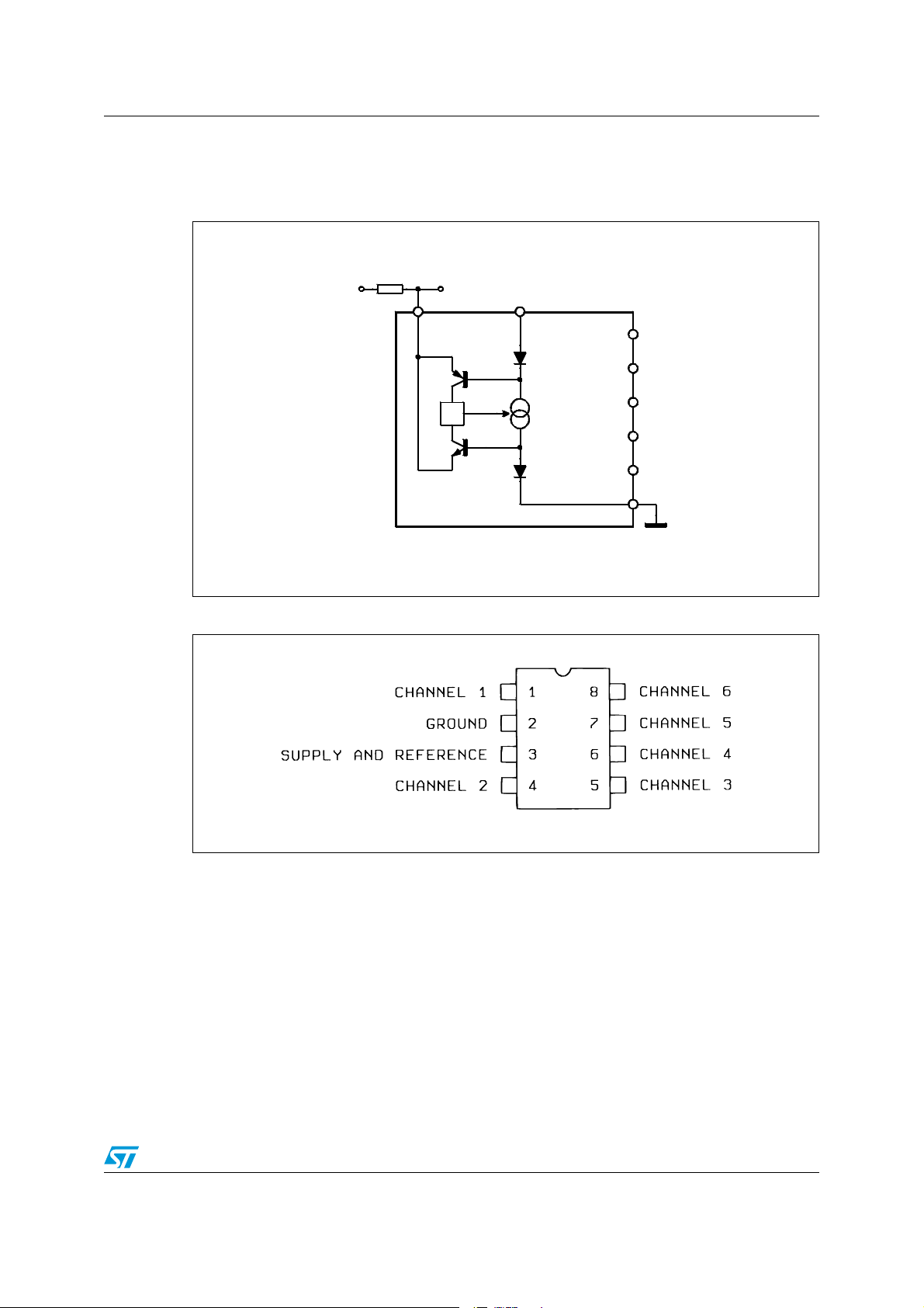
L9700D-E Block diagram and pin connection
7
$$
7
065
7
*/
34
*
#
-%&
("1($'5
1 Block diagram and pin connection
Figure 1. Block diagram
Figure 2. Pin connection
("1($'5
Doc ID 022301 Rev 1 5/14
Page 6

Electrical specification L9700D-E
2 Electrical specification
2.1 Absolute maximum ratings
Stressing the device above the rating listed in
Ta bl e 2
may cause permanent damage to the
device. These are stress ratings only and operation of the device at these or any other
conditions above those indicated in the operating sections of this specification is not implied.
Exposure to the conditions in table below for extended periods may affect device reliability.
Table 2. Absolute maximum ratings
Symbol Parameter Value Unit
V
I
Tj, T
P
Supply voltage 20 V
CC
Input current per channel 30 mA
IN
Junction and storage temperature -55 to 150 °C
stg
Total power dissipation (T
tot
= 85°C) 650 mW
amb
Note: The circuit is ESD protected according to MIL-STD-883C
2.2 Thermal data
Table 3. Thermal data
Symbol Parameter Value Unit
R
thj-amb
Thermal resistance junction-ambient (max) 200 °C/W
6/14 Doc ID 022301 Rev 1
Page 7

L9700D-E Electrical specification
2.3 Electrical characteristics
VCC = 5 V; Tj= -40 to 125°C, unless otherwise specified.
Table 4. Power section
Symbol Parameter Test conditions Min. Typ. Max. Unit
V
Supply voltage 4.75 5.25 V
CC
I
Supply current 1.5 3 mA
CC
Static input clamping
V
cis
voltage
Negative I
Positive I
VIN= 0 15 µA
= -10 mA –250 0 mV
IN
=10mA V
IN
CC
VCC+250 mV
I
Input current (static)
IN
V
IN=VCC
V
=50mV 5 µA
IN
15 µA
VIN=VCC-50mV 5 µA
IIN=±10mA; tR=5ns
Dynamic input clamping
(1)
V
cld
voltage
Positive overshoot
=±10mA; tR=5ns
I
IN
Negative overshoot
(1)
Setting time See
t
S
(1)
R
1. Design limits are guaranteed by statistical control on production samples over the indicated temperature
Dynamic input resistance 5 Ω
IN
and supply voltage ranges. These limits are not used to calculate outgoing quality levels.
Figure 4
400 mV
400 mV
20 ns
Figure 3. DC input characteristic limit points of the characteristic approximation
("1($'5
Doc ID 022301 Rev 1 7/14
Page 8

Electrical specification L9700D-E
Figure 4. Dynamical input characteristics (part 1/2)
("1($'5
Figure 5. Dynamical input characteristics (part 2/2)
("1($'5
8/14 Doc ID 022301 Rev 1
Page 9

L9700D-E Application information
3 Application information
Figure 6. Typical application
7
$$
%*(*5"-
*/1654
"/"-0(
*/1654
34
$*/
-%&
.*$30
$0.165&3
O'
("1($'5
Most integrated circuits, both HNMOS and bipolar, are very sensitive to positive and
negative overvoltages on the supply and at the inputs.
These transients occur in large numbers and with different magnitudes in the automotive
environment, making adequate protection for devices aimed at it indispensable.
Overvoltages on the supply line are faced through high voltage integration technologies or
through external protection (transil, varistor).
Signal inputs are generally protected using clamp diodes to the supply and ground, and a
current limiter resistor. However, such solutions do not always completely satisfy the
protection specifications in terms of intervention speed, negative clamping and current
leakage high enough to change analog signals.
The L9700D-E device combines a high intervention speed with a high precision positive and
negative clamp and a low current leakage providing the optimal solution to the problems of
the automotive environment.
The high intervention speed, due to the pre-bias of the limiter stage and internal feedback,
limits the voltage overshoot and avoid the use of external capacitors for the limitation of the
transient rise times.
Figure 6
illustrates a typical automotive application scheme. The resistor RS limits the input
current of the device and is therefore dimensioned considering the characteristics of the
transients to be eliminated.
Consequently:
V
transient Peak
------------------------------------
R
S
Doc ID 022301 Rev 1 9/14
I
IN MAX
=
Page 10

Application information L9700D-E
The CIN capacitors must be used only on analog inputs because they present a low
impedance during the sampling period.
The minimum value for C
is determined by the accuracy required, the time taken to
IN
sample the input and the input impedance during that time, while the maximum value is
determined by the required frequency response and the value of R
.
S
Thus for a resistive input A/D connector where:
T
= sample time (seconds)
S
R
= device input resistance (Ohms)
D
V
= input voltage (Volts)
IN
k = required accuracy (%)
Q
= charge on capacitor before sampling
1
Q
= charge on capacitor after sampling
2
I
= device input current (Amps)
D
Thus:
Q1Q
–
but Q1 = CIN V
and Q1 – Q2 = ID – T
C
C
IN
I
DTS
min()
IN
min()
so that
and
so
2
IN
kCINVIN–⋅
-------------------------------- -=
⋅
kQ
-------------- -=
100
S
100
I
⋅
DTS
---------------- -
V
IN
100 T
⋅
---------------------
⋅
kR
D
1
Farad=
k⋅
S
Farad=
The calculation for a sample and hold type convertor is even simpler:
k = required accuracy (%)
C
= hold capacitor (farad)
H
C
min()
IN
10/14 Doc ID 022301 Rev 1
100 C
⋅
----------------------
k
H
Farad=
Page 11

L9700D-E Package and packing information
4 Package and packing information
4.1 ECOPACK
In order to meet environmental requirements, ST offers these devices in different grades of
ECOPACK
specifications, grade definitions and product status are available at: www.st.com
ECOPACK
®
®
packages, depending on their level of environmental compliance. ECOPACK®
®
is an ST trademark.
4.2 Package mechanical data
Figure 7. SO-8 package dimensions
EH
'
0
D
.
/
&
$
6
(H
F
D
D
E
Doc ID 022301 Rev 1 11/14
)
("1($'5
Page 12

Package and packing information L9700D-E
Table 5. SO-8 mechanical data
mm.
Dim.
Min. Typ. Max.
A 1.75
a1 0.1 0.25
a2 1.65
a3 0.65 0.85
b0.35 0.48
b1 0.19 0.25
C 0.25 0.5
c1 45° (typ.)
D4.8 5.0
E5.8 6.2
e1.27
e3 3.81
F3.8 4.0
L 0.4 1.27
M 0.6
S8° (max.)
12/14 Doc ID 022301 Rev 1
Page 13

L9700D-E Revision history
5 Revision history
Table 6. Document revision history
Date Revision Changes
05-Oct-2011 1 Initial release.
Doc ID 022301 Rev 1 13/14
Page 14

L9700D-E
Please Read Carefully:
Information in this document is provided solely in connection with ST products. STMicroelectronics NV and its subsidiaries (“ST”) reserve the
right to make changes, corrections, modifications or improvements, to this document, and the products and services described herein at any
time, without notice.
All ST products are sold pursuant to ST’s terms and conditions of sale.
Purchasers are solely responsible for the choice, selection and use of the ST products and services described herein, and ST assumes no
liability whatsoever relating to the choice, selection or use of the ST products and services described herein.
No license, express or implied, by estoppel or otherwise, to any intellectual property rights is granted under this document. If any part of this
document refers to any third party products or services it shall not be deemed a license grant by ST for the use of such third party products
or services, or any intellectual property contained therein or considered as a warranty covering the use in any manner whatsoever of such
third party products or services or any intellectual property contained therein.
UNLESS OTHERWISE SET FORTH IN ST’S TERMS AND CONDITIONS OF SALE ST DISCLAIMS ANY EXPRESS OR IMPLIED
WARRANTY WITH RESPECT TO THE USE AND/OR SALE OF ST PRODUCTS INCLUDING WITHOUT LIMITATION IMPLIED
WARRANTIES OF MERCHANTABILITY, FITNESS FOR A PARTICULAR PURPOSE (AND THEIR EQUIVALENTS UNDER THE LAWS
OF ANY JURISDICTION), OR INFRINGEMENT OF ANY PATENT, COPYRIGHT OR OTHER INTELLECTUAL PROPERTY RIGHT.
UNLESS EXPRESSLY APPROVED IN WRITING BY TWO AUTHORIZED ST REPRESENTATIVES, ST PRODUCTS ARE NOT
RECOMMENDED, AUTHORIZED OR WARRANTED FOR USE IN MILITARY, AIR CRAFT, SPACE, LIFE SAVING, OR LIFE SUSTAINING
APPLICATIONS, NOR IN PRODUCTS OR SYSTEMS WHERE FAILURE OR MALFUNCTION MAY RESULT IN PERSONAL INJURY,
DEATH, OR SEVERE PROPERTY OR ENVIRONMENTAL DAMAGE. ST PRODUCTS WHICH ARE NOT SPECIFIED AS "AUTOMOTIVE
GRADE" MAY ONLY BE USED IN AUTOMOTIVE APPLICATIONS AT USER’S OWN RISK.
Resale of ST products with provisions different from the statements and/or technical features set forth in this document shall immediately void
any warranty granted by ST for the ST product or service described herein and shall not create or extend in any manner whatsoever, any
liability of ST.
ST and the ST logo are trademarks or registered trademarks of ST in various countries.
Information in this document supersedes and replaces all information previously supplied.
The ST logo is a registered trademark of STMicroelectronics. All other names are the property of their respective owners.
© 2011 STMicroelectronics - All rights reserved
STMicroelectronics group of companies
Australia - Belgium - Brazil - Canada - China - Czech Republic - Finland - France - Germany - Hong Kong - India - Israel - Italy - Japan -
Malaysia - Malta - Morocco - Philippines - Singapore - Spain - Sweden - Switzerland - United Kingdom - United States of America
www.st.com
14/14 Doc ID 022301 Rev 1
 Loading...