How it Works
Log In / Sign Up
Buy Points
How it Works
FAQ
Contact Us
Questions and Suggestions
Users
Datasheet
Loading...
L
L934SYD
L934SYT
L934VGC-E
L934YC
L934YD
L934YD12V
L934YD5V
L934YT
L9351
L9352B
L9352DIE1
L9362
L9374
L9377DIE1
L937EGW
L937EYW
L937GGD
L937GYW
L937IID
L937YYD
L9380
2
L9386
L9386MD
L9389
L9390
2
L9396
L93PI
L9404
L9407F
L9409
L9444VB
L9448VB
L9466
L9473
L9480VB
L9484
L9524C
L9610C
L9611C
L9613
L9613B
L9615
L9616
L9616D
L9637
2
L9637D
L9637D013TR
L9639
L964YV-SGD-0L
L9651
L9659
L9669
L9686
L9700
L9700D-E
L9703
L9703D
L9704
L9704D
L9705D
L9733
L9758
L9805
L9805E
L9820
L9820D
L9821
L9822E
L9822ED
L9822EPD
L9822N
L9823
2
L9825
L9826
2
L9848
L9856
L98SI
L9903
L9904
L9907ND
L9911
L9925
L9930
L9935
2
L9937
L9942
L9947
L9949
L9950
L9950XP
L9951
2
L9951XP
L9952GXP
L9953
L9953LXP
L9953XP
L9954
L9954LXP
L9954XP
L9958
Loading...
Loading...
Nothing found
L9659
Datasheet (ST)
51 pgs
573.58 Kb
0
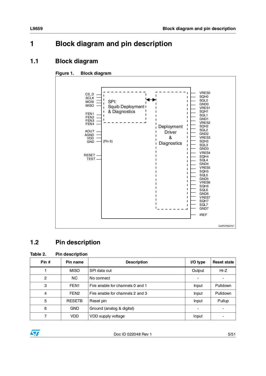
Table of contents
Loading...
Datasheet L9659 Datasheet (ST)
...
Datasheet Datasheet (ST)
Download
Specifications and Main Features
Frequently Asked Questions
User Manual
Download
Loading...
+
hidden pages
Unhide
You need points to download manuals.
1 point = 1 manual.
You can buy points or you can get point for every manual you upload.
Buy points
Upload your manuals
 Loading...

")