

Page 1
Features
■ Quad gate driver for external N-channel Power
MOSFETs in high-side configuration:
– Gates driven by PWM output signal
– Adjustable gate charge/discharge currents
– Limited gate-to-source voltages
– Negative clamping for inductive loads
– Advanced run-off control
– Regulation of the power through the glow
plugs
■ Control output for external relay driver
■ Battery-voltage-compatible two-wire interface
■ Supply voltage monitoring with shutdown
■ Battery voltage monitoring with shutdown
■ Junction temperature monitoring with
shutdown
■ Monitoring of currents through the glow plugs
with shutdown at overcurrent (adjustable
threshold)
■ Monitoring of external switches
■ Charge pump voltage monitoring with
shutdown
■ Active clamping during load dump
Table 1. Device summary
L9524C
Glow plug system control IC
SO24
Description
The L9524C is a control IC for up to six glow
plugs of diesel engines. The glow plugs are
switched by up to four external PWM-controlled
N-channel Power MOSFETs or a single relay in
high-side configuration.
Supply voltage, battery voltage, junction
temperature, switches, currents through the glow
plugs, and charge pump voltage are monitored.
A two-wire interface is used to communicate with
the diesel engine management system.
Order code Package Packing
L9524C SO24 Tube
L9524C-TR SO24 Tape and reel
January 2008 Rev 3 1/27
www.st.com
1
Page 2

Contents L9524C
Contents
1 Block diagram . . . . . . . . . . . . . . . . . . . . . . . . . . . . . . . . . . . . . . . . . . . . . . 5
2 Pins description . . . . . . . . . . . . . . . . . . . . . . . . . . . . . . . . . . . . . . . . . . . . 6
3 Electrical specifications . . . . . . . . . . . . . . . . . . . . . . . . . . . . . . . . . . . . . . 7
3.1 Absolute maximum ratings . . . . . . . . . . . . . . . . . . . . . . . . . . . . . . . . . . . . . 7
3.2 Thermal data . . . . . . . . . . . . . . . . . . . . . . . . . . . . . . . . . . . . . . . . . . . . . . . 7
3.3 Electrical characteristics . . . . . . . . . . . . . . . . . . . . . . . . . . . . . . . . . . . . . . . 8
4 Functional description . . . . . . . . . . . . . . . . . . . . . . . . . . . . . . . . . . . . . . 12
4.1 Operating modes . . . . . . . . . . . . . . . . . . . . . . . . . . . . . . . . . . . . . . . . . . . 12
4.2 Supply . . . . . . . . . . . . . . . . . . . . . . . . . . . . . . . . . . . . . . . . . . . . . . . . . . . 13
4.3 Control input . . . . . . . . . . . . . . . . . . . . . . . . . . . . . . . . . . . . . . . . . . . . . . . 14
4.4 Diagnostic output . . . . . . . . . . . . . . . . . . . . . . . . . . . . . . . . . . . . . . . . . . . 15
4.5 Current monitoring . . . . . . . . . . . . . . . . . . . . . . . . . . . . . . . . . . . . . . . . . . 17
4.6 Switch monitoring . . . . . . . . . . . . . . . . . . . . . . . . . . . . . . . . . . . . . . . . . . . 18
4.7 Thermal shutdown . . . . . . . . . . . . . . . . . . . . . . . . . . . . . . . . . . . . . . . . . . 18
4.8 Gate drivers . . . . . . . . . . . . . . . . . . . . . . . . . . . . . . . . . . . . . . . . . . . . . . . 18
4.9 Relay output . . . . . . . . . . . . . . . . . . . . . . . . . . . . . . . . . . . . . . . . . . . . . . . 19
4.10 Gate charge/discharge current variation . . . . . . . . . . . . . . . . . . . . . . . . . 19
4.11 Overcurrent threshold variation . . . . . . . . . . . . . . . . . . . . . . . . . . . . . . . . 19
4.12 Advanced run-off control . . . . . . . . . . . . . . . . . . . . . . . . . . . . . . . . . . . . . 20
4.13 Output timing . . . . . . . . . . . . . . . . . . . . . . . . . . . . . . . . . . . . . . . . . . . . . . 20
4.14 Power regulation . . . . . . . . . . . . . . . . . . . . . . . . . . . . . . . . . . . . . . . . . . . . 21
5 Application diagrams . . . . . . . . . . . . . . . . . . . . . . . . . . . . . . . . . . . . . . . 22
6 Package information . . . . . . . . . . . . . . . . . . . . . . . . . . . . . . . . . . . . . . . . 25
7 Revision history . . . . . . . . . . . . . . . . . . . . . . . . . . . . . . . . . . . . . . . . . . . 26
2/27
Page 3

L9524C List of tables
List of tables
Table 1. Device summary . . . . . . . . . . . . . . . . . . . . . . . . . . . . . . . . . . . . . . . . . . . . . . . . . . . . . . . . . . 1
Table 2. Pins description . . . . . . . . . . . . . . . . . . . . . . . . . . . . . . . . . . . . . . . . . . . . . . . . . . . . . . . . . . 6
Table 3. Absolute maximum ratings . . . . . . . . . . . . . . . . . . . . . . . . . . . . . . . . . . . . . . . . . . . . . . . . . . 7
Table 4. Thermal data. . . . . . . . . . . . . . . . . . . . . . . . . . . . . . . . . . . . . . . . . . . . . . . . . . . . . . . . . . . . . 7
Table 5. Electrical characteristics . . . . . . . . . . . . . . . . . . . . . . . . . . . . . . . . . . . . . . . . . . . . . . . . . . . . 8
Table 6. Mode. . . . . . . . . . . . . . . . . . . . . . . . . . . . . . . . . . . . . . . . . . . . . . . . . . . . . . . . . . . . . . . . . . 12
Table 7. Go / no-go protocol description. . . . . . . . . . . . . . . . . . . . . . . . . . . . . . . . . . . . . . . . . . . . . . 16
Table 8. Failure register description . . . . . . . . . . . . . . . . . . . . . . . . . . . . . . . . . . . . . . . . . . . . . . . . . 16
Table 9. Sense input pin connection. . . . . . . . . . . . . . . . . . . . . . . . . . . . . . . . . . . . . . . . . . . . . . . . . 17
Table 10. Document revision history . . . . . . . . . . . . . . . . . . . . . . . . . . . . . . . . . . . . . . . . . . . . . . . . . 26
3/27
Page 4

List of figures L9524C
List of figures
Figure 1. Block diagram . . . . . . . . . . . . . . . . . . . . . . . . . . . . . . . . . . . . . . . . . . . . . . . . . . . . . . . . . . . . 5
Figure 2. Pin connection (top view) . . . . . . . . . . . . . . . . . . . . . . . . . . . . . . . . . . . . . . . . . . . . . . . . . . . 6
Figure 3. Shunt sense versus transistor sense . . . . . . . . . . . . . . . . . . . . . . . . . . . . . . . . . . . . . . . . . 13
Figure 4. Control input signal in transistor mode (modes 3 to 6) . . . . . . . . . . . . . . . . . . . . . . . . . . . . 14
Figure 5. Permanent switch on of glow plugs at first falling edge in transistor mode (modes 3 to 6) 14
Figure 6. Control input signal in mode 2 for permanent switch on . . . . . . . . . . . . . . . . . . . . . . . . . . . 15
Figure 7. Serial diagnostic interface protocol. . . . . . . . . . . . . . . . . . . . . . . . . . . . . . . . . . . . . . . . . . . 17
Figure 8. Timing diagram of advanced run-off control . . . . . . . . . . . . . . . . . . . . . . . . . . . . . . . . . . . . 20
Figure 9. Output timing . . . . . . . . . . . . . . . . . . . . . . . . . . . . . . . . . . . . . . . . . . . . . . . . . . . . . . . . . . . 20
Figure 10. Mode 1: relay mode, go/no-go diagnostic interface protocol . . . . . . . . . . . . . . . . . . . . . . . 22
Figure 11. Mode 2: relay mode, serial diagnostic interface protocol . . . . . . . . . . . . . . . . . . . . . . . . . . 22
Figure 12. Mode 3: transistor mode, shunt sense, no power regulation . . . . . . . . . . . . . . . . . . . . . . . 23
Figure 13. Mode 4: transistor mode, shunt sense, power regulation . . . . . . . . . . . . . . . . . . . . . . . . . . 23
Figure 14. Mode 5: transistor mode, transistor sense, no power regulation . . . . . . . . . . . . . . . . . . . . 24
Figure 15. Mode 6: transistor mode, transistor sense, power regulation . . . . . . . . . . . . . . . . . . . . . . . 24
Figure 16. SO24 mechanical data and package dimensions. . . . . . . . . . . . . . . . . . . . . . . . . . . . . . . . 25
4/27
Page 5
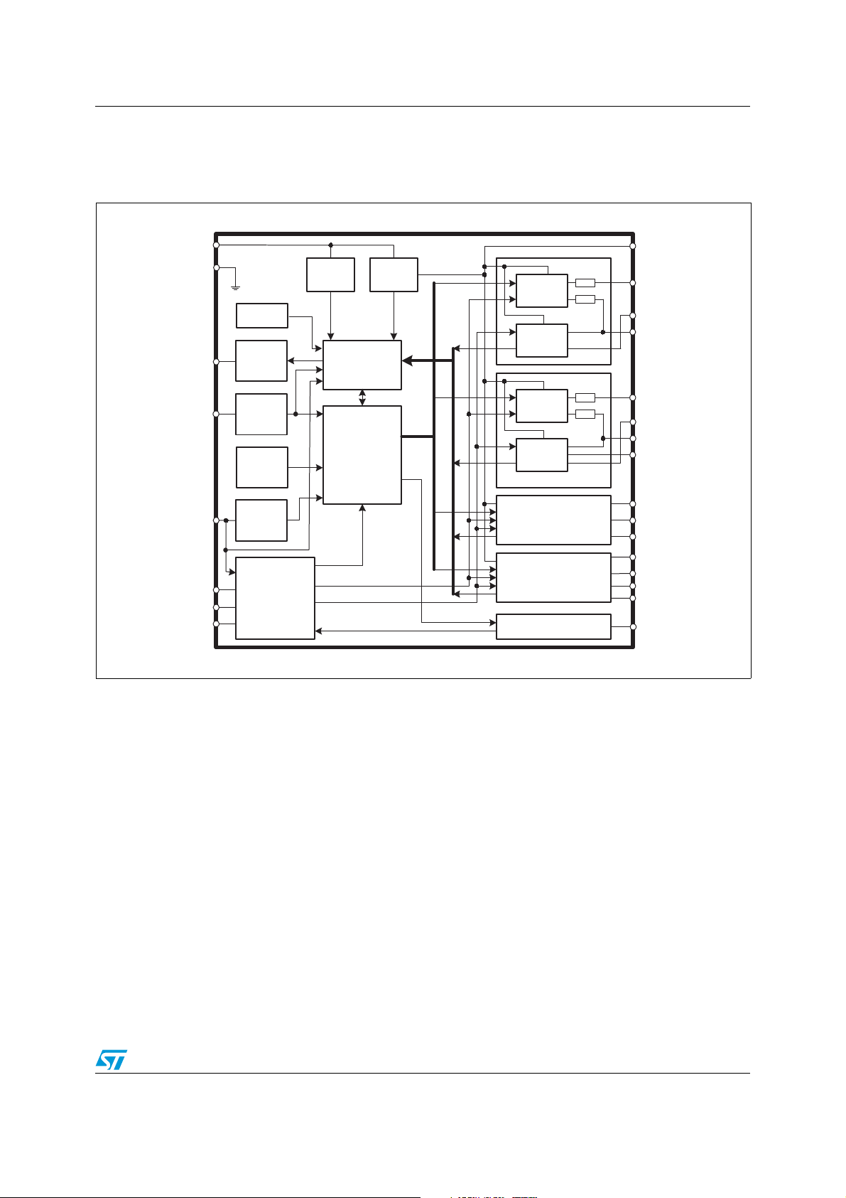
L9524C Block diagram
1 Block diagram
Figure 1. Block diagram
VS
GND
DO
BAT
MS
CUR
OCT
CP
Supply
voltage
monitor
Thermal
shutdown
Diagnostic
output
CI
Control
input
Reference
oscillator
Voltage
controlled
oscillator
Program
Charge/discharge current
Charge
Diagnostic
logic
Control
logic
Overcurrent threshold
pump
Gate
driver
Failure
monitor
monitor
(same as channel 1)
(same as channel 2)
Mode input / relay output
Gate
driver
Failure
Channel 3
Channel 4
Channel 1
Channel 2
G1
SP1
SN1
G2
SP2
SN2
SN5
G3
SP3
SN3
G4
SP4
SN4
SN6
IO
5/27
Page 6
Pins description L9524C
2 Pins description
Figure 2. Pin connection (top view)
Table 2. Pins description
SP1
G1
SN1
SP2
G2
SN5
SN2
BAT
DO GND
VS MS
CP CUR
OCT IO
1
2
3
4
5
6
7
8
9
10
11
SO24
24
SP3
23
G3
22
SN3
21
SP4
20
G4
19
SN6
18
SN4
17
CI
16
15
14
1312
Pins # Name Function
1 SP1 Positive sense input, glow plug 1
2 G1 Driver output for external high-side power MOSFET, transistor 1
3 SN1 Negative sense input, glow plug 1
4 SP2 Positive sense input, glow plugs 2 and 5
5 G2 Driver output for external high-side power MOSFET, transistor 2
6 SN5 Negative sense input, glow plug 5
7 SN2 Negative sense input, glow plug 2
8 BAT Battery voltage input
9 DO Diagnostic output
10 VS Supply voltage input
11 CP Charge pump output
12 OCT Overcurrent threshold setting
13 IO
Transistor mode: input for selection of power regulation feature
Relay mode: output to control external relay driver
14 CUR Power MOSFET gate charge/discharge current setting
15 MS
Mode selection input: transistor modes (transistor sense / shunt sense) / relay mode
16 GND Ground pin
17 CI Control input
18 SN4 Negative sense input, glow plug 4
19 SN6 Negative sense input, glow plug 6
20 G4 Driver output for external high-side power MOSFET, transistor 4
21 SP4 Positive sense input, glow plugs 4 and 6
22 SN3 Negative sense input, glow plug 3
23 G3 Driver output for external high-side power MOSFET, transistor 3
24 SP3 Positive sense input, glow plug 3
6/27
Page 7
L9524C Electrical specifications
3 Electrical specifications
3.1 Absolute maximum ratings
Table 3. Absolute maximum ratings
Symbol Parameter Value Unit
|dV
V
BAT
V
V
V
OCT
VMS, V
V
DO
V
VS
VS
V
CP
, VCI,
SP1-4
SN1-6
, V
, V
Supply voltage range -0.3 to 45 V
/dt| Supply voltage slope 10 V/μs
Charge pump voltage range -0.3 to 45 V
,
Input pin voltage range (BAT, CI, SP1-4, SN1-6) -16 to 45 V
,
CUR
Input pin voltage range (OCT, CUR, MS, IO) -0.3 to 7 V
IO
Output pin voltage range (DO, G1-4) -16 to 45 V
G1-4
Warning: The device may become damaged if using externally applied
All the pin of the IC are protected against ESD. the verification is performed according to:
AEC Q100-002 (HBM) and AEC Q100-011 (CDM).
3.2 Thermal data
Table 4. Thermal data
voltages or currents exceeding these limits!
Symbol Parameter Value Unit
T
T
JSD
Operating junction temperature -40 to 125 °C
J
Junction temperature thermal shutdown threshold 125 to 150 °C
7/27
Page 8
Electrical specifications L9524C
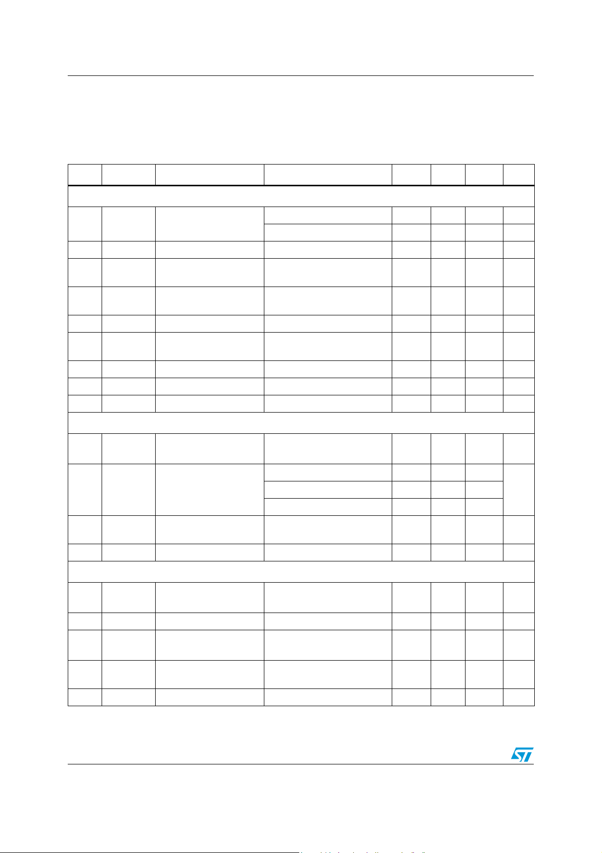
3.3 Electrical characteristics
5V ≤ VVS;V
≤ 18V, -40°C ≤ TJ ≤ 125°C, unless otherwise specified. The voltages are
BAT
referred to GND and currents are assumed positive, when current flows into the pin.
Table 5. Electrical characteristics
Item Symbol Parameter Test condition Min. Typ. Max. Unit
Supply (VS)
1.1 I
1.2 V
1.3 V
1.4 V
1.5 V
1.6 V
1.7 V
1.8 t
1.9 t
Supply (BAT)
VS
VS uv
VS uvh
VS ol
VS ov
VS ovh
VS ld
VS fil
VS ld
Supply current
1520mA
= 12V 1 10 mA
V
S
Undervoltage threshold 4 5 V
Undervoltage threshold
hysteresis
(1)
Open-load detection
threshold
100 400 mV
5.5 7.2 V
Overvoltage threshold 18 22 V
Overvoltage threshold
hysteresis
(1)
0.4 1.6 V
Load dump threshold 28 35 V
Filter time
Load dump delay time
(2)
(1)
12ms
10 μs
2.1 I
2.2 R
2.3 V
2.4 t
BAT leak
BAT
BAT uv
BAT fil
Charge pump (CP)
3.1 V
3.2 I
3.3 V
3.4 f
3.5 t
CP
CP
CP uv
CP
CP fil
V
≤ 3V
Leakage current
VS
0V ≤ V
BAT
≤ 12V
05μA
-40°C 25 43 150
Internal pull-down
resistance
kΩ30°C 25 65 150
125°C 25 106 150
Battery undervoltage
threshold
Filter time
(2)
Charge pump voltage ICP = -100μA
> V
V
MS
(transistor mode) 1 2 V
MS tr
300 760 μs
V
VS
+5V
V
VS
+18V
Charging current VCP = VVS + 5V -1500 -100 μA
Charge pump
undervoltage threshold
Charge pump frequency
(1)
Filter time
(2)
V
VS
+3.5V
0.6 7 MHz
400 950 μs
V
VS
+5V
8/27
Page 9
L9524C Electrical specifications
Table 5. Electrical characteristics (continued)
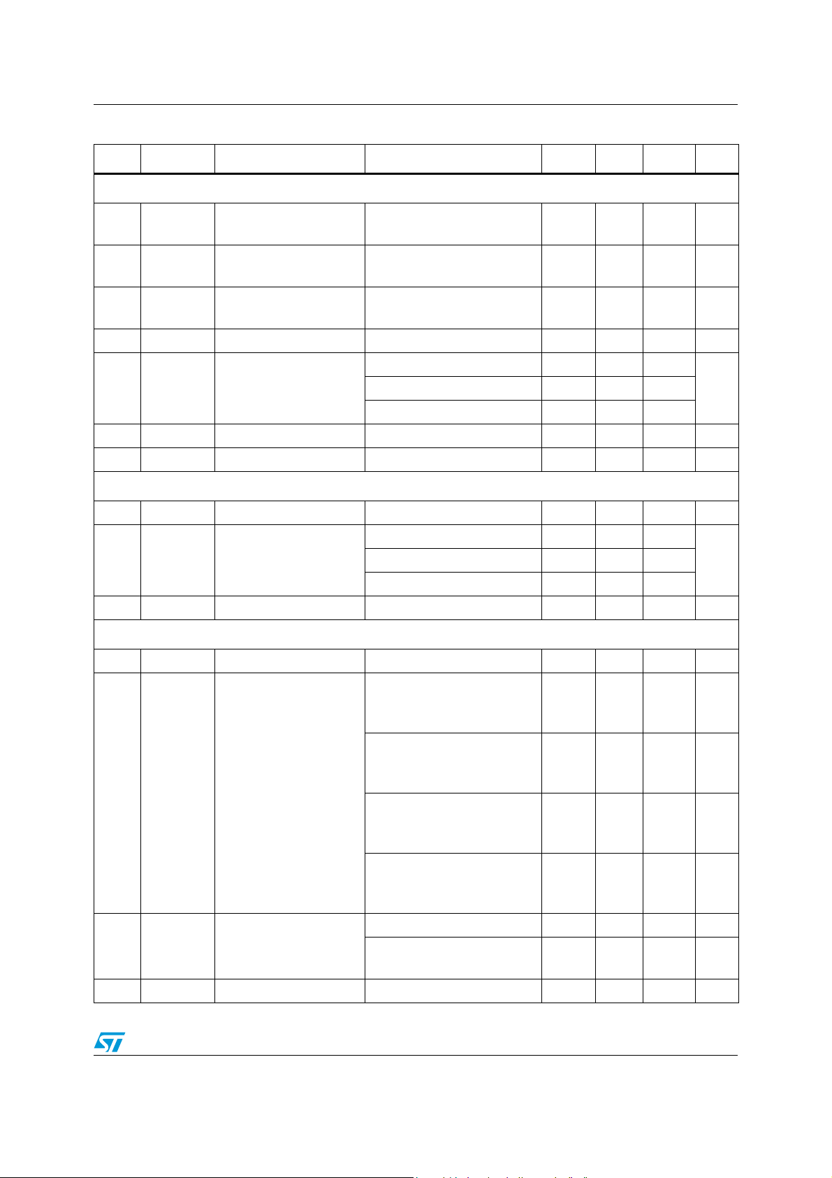
Item Symbol Parameter Test condition Min. Typ. Max. Unit
Control input (CI)
4.1 V
4.2 V
4.3 V
4.4 V
4.5 R
4.6 t
4.7 t
CI off
CI on
CI h
CI to
CI
CI fil
CI to
Input “off” level
Input “on” level
Off-to-on hysteresis
(1)
Input “timeout” threshold 1 1.6 V
≤ VVS; -40°C 20 35 120
V
Internal pull-up
resistance
Filter time
(2)
PWM time-out
(2)
CI
≤ VVS; 30°C 20 53 120
CI
≤ VVS; 125°C 20 87 120
V
CI
0.6 ·
V
VS
0.4 ·
V
VS
0.03 ·
V
VS
0.04 ·
V
VS
0.05 ·
V
VS
0.5 1 ms
50 100 ms
Diagnostic output (DO)
5.1 V
DOL
Output low voltage VVS ≥ 4.5V; IDO ≤ 5mA 0.3 1.5 V
VDO ≤ VVS; -40°C 20 30 120
5.2 R
5.3 I
DO max
DO
Internal pull-up
resistance
≤ VVS; 30°C 20 45 120
DO
V
≤ VVS; 125°C 20 74 120
DO
Current limitation 5 20 mA
Monitoring of currents through glow plugs (SP1-SN1, SP2-SN2, SP3-SN3, SP4-SN4, SP2-SN5, SP4-SN6)
kΩV
kΩV
6.1 ΔV
6.2 ΔV
6.3 TC
6.4 t
OL fil
OL
OC 0
OC
Open-load threshold 6V ≤ V
1.5V ≤ V
VMS < V
OCT pin open
1.5V ≤ V
< V
V
MS
0V ≤ V
Overcurrent threshold
1.5V ≤ V
V
MS>VMS tc
ϑ = -40°C; OCT pin open
1.5V ≤ V
VMS>V
ϑ = -40°C; 0V ≤ V
VMS < V
Overcurrent threshold
temperature coefficient
VMS>V
OCT pin open
Open-load filter time
(2)
VMS > V
SPX;VSNX
SPX;VSNX
MS tc
SPX;VSNX
MS tc
OCT
SPX;VSNX
SPX;VSNX
MS tc
MS tc
MS tc
MS tr
≤ VVS + 3V 6.7 14.7 mV
≤ VVS + 3V
(shunt sense)
≤ VVS + 3V
(shunt sense)
≤ V
CUR
150 185 mV
V
OCT
0.385
·
V
OCT
0.445
·
≤ VVS + 3V
(transistor sense)
≤ VVS + 3V
(transistor sense)
≤ V
OCT
CUR
(shunt sense)
(transistor sense)
150 290 mV
V
·
OCT
0.345
1)
0K
0.008 0.012 K
V
OCT
0.485
·
(transistor mode) 1 2 ms
9/27
-1
-1
Page 10

Electrical specifications L9524C
Table 5. Electrical characteristics (continued)
Item Symbol Parameter Test condition Min. Typ. Max. Unit
6.5 t
OC fil
Overcurrent filter time
Monitoring of external switches (SN1, SN2, SN3, SN4)
7.1 V
SD
Switch defect threshold
(2)
400 950 μs
V
VS
0.4
·
VVS ·
0.6
7.2 t
SD fil
Switch defect filter time
(2)
Gate driver outputs (G1, G2, G3, G4)
8.1 V
8.2 V
8.3 V
8.4 I
8.5 I
G off
G on
G cl
G off
G on
8.6 Slope
8.7 R
8.8 Δt
G on
Gate off voltage IGX ≤ 100μAV
Gate on voltage V
Gate clamping voltage V
Gate discharge current I
Gate charge current I
Gate charge- dischargecurrent I
Output resistance
G
G/ICUR
(1)
Jitter of output on time -300 300 μs
Mode input / relay output (IO)
9.1 V
9.2 R
9.3 I
9.4 I
IO max
9.5 V
9.6 t
IO sup
IO on
IO
IO pr
Output on voltage IIO ≥ -100μA36V
Output resistance IIO ≥ -1mA 100 500 W
IO
Input pull-down current
Current limitation -25 -5 mA
Power regulation
threshold
Pulse suppress time
(2)
Positive sense inputs (SP1, SP2, SP3, SP4)
12ms
V
SNX
V
= V
SNX
SNX
CUR
CUR
-250μA ≤ I
VS
= -20V -18 -16 V
= -125µA 270 540 µA
= -125µA 270 540 µA
≤ -70µA 2.33 4.33
CUR
VS
+5V
SNX
+0.7V
V
VS
+10V
1kΩ
VIO ≥ 1V 25 100 μA
= 0V 50 500 μA
V
VS
12V
2.5 5 ms
10.1 I
10.2 I
SP leak
SP
Leakage current VVS ≤ 3V 0 5 μA
Input pull-down current V
SNX
6V ≤ V
= V
SNX
-40°C
10.3 R
SP1-4
Pull-down resistor
35°C 40 150 270
125°C 40 220 270
Negative sense inputs (SN1, SN2, SN3, SN4, SN5, SN6)
11.1 I
SN
Input pull-down current V
SNX
= V
10/27
≥ 6V 15 780 μA
SPX
= V
SPX
≤ 20V
SPX
40 100 270
≥ 6V 15 780 μA
kΩ
Page 11

L9524C Electrical specifications
Table 5. Electrical characteristics (continued)
Item Symbol Parameter Test condition Min. Typ. Max. Unit
SNX
= V
6V ≤ V
-40°C
11.2 R
SN1-6
Pull down resistor
35°C 40 150 270
125°C 40 220 270
Overcurrent threshold setting (OCT)
12.1 I
OCT
Input pull-up current
VVS ≥ 6V
= 3.5V
V
OCT
Power MOSFET gate charge/discharge current setting (CUR)
13.1 V
13.2 I
CUR max
CUR
Output voltage I
Current limitation V
≥ -150μA 2.35 2.5 2.65 V
CUR
≤ 2V -500 -250 μA
CUR
Input pin for mode selection (MS)
14.1 I
14.2 V
14.3 V
MS
MS tr
MS tc
Pull-up current VMS = 3V -60 -15 μA
Transistor mode
threshold
Temperature
compensation threshold
V
≥ 6V 3 4 V
VS
Output timing
15.1 t
15.2 t
15.3 t
del
gap
sup
Delay time
Gap between channels
(2)
Failure suppress time
(2)
(2)
Power regulation
SPX
≤ 20V
40 100 270
kΩ
-40 -10 μA
12V
2.5 5 ms
50 250 μs
400 950 μs
8V ≤ V
30ms ≤ T
16.1 ΔV
RMS
Accuracy
t
CI on/TCI
< 70°C
> 70°C -2 2
1. not tested, guaranteed by design
2. time constants created digitally, verified by scan path test
≤ 16V
BAT
≤ 33ms
CI
≥ 20%
-1.5 1.5%
% ·
V
RMSref
11/27
Page 12

Functional description L9524C
4 Functional description
4.1 Operating modes
The L9524C can operate in a total of 6 modes. The selection is done by short-circuiting the
appropriate pins and voltages as shown in the following table:
Table 6. Mode
Mode Description MS pin BAT pin IO pin CI pin
1 relay mode, go/no-go diagnostic interface protocol ground ground output statical signal
2 relay mode, serial diagnostic interface protocol ground battery output PWM signal
3 transistor mode, shunt sense, no power regulation CUR pin battery
4 transistor mode, shunt sense, power regulation CUR pin battery ground PWM signal
5 transistor mode, transistor sense, no power regulation open battery
6 transistor mode, transistor sense, power regulation open battery ground PWM signal
CUR
pin
CUR
pin
PWM signal
PWM signal
Modes 1 and 2 are for relay usage (referred to as “relay mode”) and modes 3 to 6 for
transistors usage (referred to as “transistor mode”).
In relay mode the protocol of the diagnostic interface (DO pin) can be selected from go/nogo protocol and serial protocol (see section “Diagnostic output” for protocol description).
In transistor mode the protocol of the diagnostic interface is the serial protocol. It can be
distinguished between using shunts for monitoring the current through the glow plugs
(referred to as “shunt sense”) or using the R
of the power MOSFET’s themselves
DS(on)
(referred to as “transistor sense”). In shunt sense mode the resistance of the shunt is
assumed to be constant with respect to the temperature while in transistor sense mode the
R
of the power MOSFET’s is assumed to vary with respect to the temperature and
DS(on)
therefore overcurrent monitoring is adjusted appropriately.
In transistor mode there are two possibilities to control the output timing. In modes 3 and 5
the timing of the PWM control input signal determines the timing of the PWM signals applied
to the external power MOSFET’s (“no power regulation”). In modes 4 and 6 the timing of the
PWM control input signal determines the power through the glow plugs (“power regulation”)
and the timing of the PWM signals applied to the external power MOSFET’s is adjusted
depending on the battery voltage (see section “Power regulation”).
12/27
Page 13

L9524C Functional description
Figure 3. Shunt sense versus transistor sense
shunt sense transistor sense
V
BAT
V
BAT
Gx
SPx
L9524C
SNx
shunt
glow plug
SPx
Gx
L9524C
SNx
glow plug
015
4.2 Supply
The main supply pin of the L9524C is the VS pin. The voltage applied to it (VVS) is
monitored
● to switch off all glow plugs if it is less than V
failure”),
● to switch off all glow plugs if it is greater than V
failure”),
● to switch on all glow plugs if it is greater than V
during load dump”),
● to ignore open-load failures if it is less than V
Note: The glow plugs are switched on again if the corresponding switch-on condition disappears,
except if the glow plugs are switched on because of load dump. Then they remain switched
on until V
is less than V
VS
for at least t
VS ov
VS fil
In modes 2 to 6, the L9524C is additionally supplied by the BAT pin. This auxiliary supply
ensures that the external power MOSFET’s are switched off if no main supply voltage is
available at the VS pin.
VS uv
VS ov
VS ld
VS ol
.
for at least t
for at least t
for at least t
.
(“under voltage
VS fil
(“over voltage
VS fil
(“active clamping
VS ld
The BAT pin is additionally used to sense the battery voltage V
for power regulation in
BAT
modes 4 and 6 (see section “Power regulation”) and for detecting “battery under voltage
failure” (fuse between battery and module is defect) if V
t
in modes 2 to 6.
BAT fil
is less than V
BAT
BAT uv
for at least
An additional supply voltage higher than the main supply voltage is generated by an internal
charge pump which charges an external storage capacitor connected to the CP pin. This
capacitor mainly supplies the gates of the external n-channel power MOSFET’s. The charge
pump voltage V
for at least t
off even if the charge pump voltage becomes greater than V
is monitored and the glow plugs are switched off if it is less than V
CP
(“charge pump under voltage”). Afterwards, the glow plugs remain switched
CP fil
until they are explicitly
CP uv
CP uv
switched on again by the CI (control input) pin.
13/27
Page 14

Functional description L9524C
4.3 Control input
The control input (CI) pin is resistively pulled up RCI to the supply voltage VVS such that
V
CI=VCI off
transitions of V
level changes of V
In transistor mode (modes 3 to 6) the L9524C expects a PWM signal at the CI pin. Each
falling edge starts measuring its on time t
low pulse) and its period T
detected if no falling edge occurs for a time greater than t
switched off. Therefore, it is not possible to switch on the glow plugs permanently with one
exception: if the low voltage level of the first falling edge is greater than V
remain switched on as long as this low pulse lasts.
Figure 4. Control input signal in transistor mode (modes 3 to 6)
and the glow plugs are switched off by default. The L9524C is controlled by
from V
CI
which last shorter than t
CI
to V
CI off
(time until next falling edge). The end of a pulse group is
CI
(falling edge) and vice versa (rising edge). Voltage
CI on
CI on
are ignored.
CI fil
(time until next rising edge, i.e. length of this
and the glow plugs are
CI to
CI to
the glow plugs
V
CI
V
CI off
0.6 . V
0.4 . V
V
CI on
glow plug
1
ON
CI on
T
CI
del
t
CI to
VS
VS
t
t
+t
CI fil
t
CI to
t
CI fil
ignored
(shorter than t
t
CI fil
+t
CI fil
t
t
CI fil
CI to
t
)
del
OFF
t
Figure 5. Permanent switch on of glow plugs at first falling edge in transistor mode
(modes 3 to 6)
V
V
CI off
0.6 . V
0.4 . V
V
CI on
V
CI to
CI
t
CI to
VS
VS
t
CI to
t
glow plug
1
ON
OFF
CI to
14/27
t
CI to
t
t
Page 15

L9524C Functional description
Though in mode 2 (relay mode, serial diagnostic interface protocol) the relay should be
switched permanently the L9524C also expects a PWM signal at the CI pin since the serial
diagnostic interface protocol is synchronized by falling edges of the CI signal (see section
“Diagnostic output”). The relay then is switched on permanently if the off time (time between
rising and falling edge) of the PWM signal is less than t
suppresses pulses shorter than t
(see section “Relay output”). For the same reason the
IO sup
since the relay output
IO sup
relay is switched off permanently if the on time (time between falling and rising edge) of the
PWM signal is less than t
. In all other cases the relay is switched according to the
IO sup
PWM signal at the CI pin.
Figure 6. Control input signal in mode 2 for permanent switch on
V
V
CI off
0.6 . V
0.4 . V
V
CI on
relay
CI
VS
VS
ON
OFF
T
CI
In mode 1 (relay mode, go/no-go diagnostic interface protocol) no edges are necessary for
the go/no-go protocol. Therefore the relay is switched on if V
if V
CI
= V
CI off
.
4.4 Diagnostic output
The diagnostic output stage of the L9524C (DO pin) consists of a current-limited low-side
switch and a pull-up resistor R
is given by the drop across the low-side switch and the voltage level of a logical high signal
is equal to V
The L9524C is able to detect the following failures (see sections “Supply”, “Current
monitoring”, and “Switch monitoring”):
● open-load (6 glow plugs),
● overcurrent (6 glow plugs, stored until power-down),
● any switch is defect (4 switches),
● supply voltage (V
● supply voltage (V
● junction temperature (T
● charge pump voltage (V
● battery voltage (V
VS
.
) is too low (“under voltage”),
VS
) is too high (“over voltage”),
VS
BAT
t
IO sup
t
CI fil+tdel
to the VS pin. The voltage level of a logical low signal V
DO
) is too high,
J
) is too low (“charge pump under voltage”), and
CP
CI
= V
t
IO sup
and it is switched off
CI on
) is too low (“battery under voltage”).
t
t
DOL
15/27
Page 16

Functional description L9524C
In order to report the occurrence of any of the above-listed failures to the diesel engine
management system the L9524C provides two protocols: go/no-go protocol for mode 1 and
serial protocol for modes 2 to 6.
The go/no-go protocol is only able to report if any of the above-listed failures occurred. This
is done according to the following table:
Table 7. Go / no-go protocol description
V
V
V
CI
CI off
CI on
VDO at “no failure” VDO at “any failure”
V
DOL
V
VS
Note: overcurrent failures are stored until power-down.
The serial protocol is able to report different kinds of failures and to assign them to the
corresponding glow plugs. Therefore, occurring failures are written into an internal 8-bit
failure register:
Table 8. Failure register description
Bit Meaning of high state
(1)
1 Open-load or overcurrent
2 Open-load or overcurrent
3 Open-load or overcurrent
4 Open-load or overcurrent
5 Open-load or overcurrent
6 Open-load or overcurrent
Overcurrent failure at any glow plug
7
battery voltage (V
BAT
One or more of the following failures (“module failure”):
any switch is defect
supply voltage (V
8
supply voltage (VVS) is too high (“overvoltage”)
) is too low (“undervoltage”)
VS
junction temperature (T
charge pump voltage (V
battery voltage (V
1. overcurrent failures are stored until power-down
2. if battery voltage is too low (“battery under voltage”) bits 7 and 8 are high
BAT
failure at glow plug 1
(1)
failure at glow plug 2
(1)
failure at glow plug 3
(1)
failure at glow plug 4
(1)
failure at glow plug 5
(1)
failure at glow plug 6
(1)
or
) is too low
) is too high
J
CP
) is too low
(2)
(“battery undervoltage”)
) is too low (“charge pump undervoltage”)
(2)
(“battery under voltage”)
V
V
VS
DOL
Bits 1 to 6 are assigned to the glow plugs. Depending on bit 7 they show open-load (bit 7 is
low) or overcurrent failures (bit 7 is high). Bit 8 shows if there is any of the listed failures
(“module failure”). In case of a battery under voltage failure bits 7 and 8 are high and all
other bits are low as long as there is no overcurrent failure stored.
For transmitting the contents of the failure register the PWM signal applied to the CI pin is
used as clock input: at any falling edge of the CI signal (see section “Control input”) the DO
pin shows the value of the next bit of the bit stream after t
16/27
DO del
.
Page 17

L9524C Functional description
Each transmission frame consists of a beginning delimiter (one low bit) followed by the 8 bits
of the failure register beginning with bit 1. After the ending delimiter (one high bit) the
diagnostic output stage is inactive and is resistively pulled up to V
VS
.
The L9524C starts transmitting the first frame at the very first falling edge of the CI signal
after power-on. Since at that time the contents of the failure register are clear the first 9 bits
(beginning delimiter followed by the contents of the 8-bit failure register) which are
transmitted are always low. The L9524C repeats transmission of the frame every 32 falling
edges of the CI signal. Only during the time when the diagnostic output stage is inactive (i.e.
between the transmission of two frames) the contents of the failure register can be written.
Figure 7. Serial diagnostic interface protocol
V
VS
...
V
CI
01234567891011
V
CI off
V
CI on
V
DO
V
VS
low
bit 1
bit 2
bit 3
V
DOL
contents of failure register
(all bits='low' at 1st frame)
delimiter
beginning
bit 4
first frame frame
4.5 Current monitoring
The L9524C is able to monitor the current through 6 glow plugs by measuring the voltage
drop across sense resistors. Therefore, there are 4 positive sense input pins (SP1, SP2,
SP3, SP4) and 6 negative sense input pins (SN1, SN2, SN3, SN4, SN5, SN6). The sense
input pins must be connected to the sense resistors according to the following table:
Table 9. Sense input pin connection
bit 5
bit 6
bit 7
bit 8
ending
high
delimiter
...
diagnostic
output
stage
inactive
31
12345678910
0
low
bit 1
bit 2
bit 3
bit 4
bit 5
contents of failure register
delimiter
beginning
bit 6
bit 7
bit 8
ending
high
delimiter
t
...
t
...
t
Sense resistor of glow plug Positive sense input pin Negative sense input pin
1SP1SN1
2SP2SN2
3SP3SN3
4SP4SN4
5SP2SN5
6SP4SN6
17/27
Page 18

Functional description L9524C
In relay mode (modes 1 and 2) the positive sense input pins are short-circuited since the
relay is the only switch. In transistor mode (modes 3 to 6) glow plug 5 is switched with
transistor 2 and glow plug 6 with transistor 4. Therefore only 4 positive sense input pins are
necessary.
If the voltage drop across the sense resistor is less than ΔV
failure is detected as long as V
for at least t
an overcurrent failure is detected and the corresponding switch is switched
OC fil
off and remains switched off until power-down. The threshold for overcurrent failures ΔV
can be varied by the voltage applied to the OCT pin (see section “Overcurrent threshold
variation”).
In modes 1 to 4 the overcurrent threshold is constant with respect to the temperature
(TC
= 0). But in modes 5 and 6 the overcurrent threshold increases linearly with the
OC
temperature ϑ to compensate the first-order temperature coefficient of the R
external power MOSFET’s which are used as sense resistors in these modes:
Equation 1
4.6 Switch monitoring
The L9524C monitors the voltages across the glow plugs (using the negative sense input
pins SN1, SN2, SN3, and SN4) to detect if the corresponding switches work properly or not.
A switch is detected as defect if it is switched on but the voltage across the corresponding
glow plug(s) is less than V
the glow plug(s) is greater than V
> V
VS
ΔV
= ΔV
OC
for at least t
SD
SD
for at least t
. If it is greater than ΔVOC (see below for definition)
VS ol
(1 + TC
OC 0
SD fil
for at least t
OC
or if it is switched off but the voltage across
SD fil
OL
(ϑ + 40°C)).
.
an open-load
OL fil
DS(on)
of the
OC
4.7 Thermal shutdown
If the junction temperature becomes greater than T
are switched on again if the junction temperature falls below T
4.8 Gate drivers
The L9524C contains four gate drivers (Gx pins) for external n-channel power MOSFET’s in
high-side configuration. Each gate driver provides a slope control by charging and
discharging the gates of the external power MOSFET’s with constant currents (I
). To adjust the slopes these currents can be varied using the CUR pin (see section “Gate
off
charge/discharge current variation”). The charging current source is supplied by an external
capacitor connected to the charge pump output (CP) pin. The gate-to-source voltages are
limited internally and without supply voltage (V
power MOSFET’s are short-circuited.
During free-wheeling of inductive loads the gates of the external power MOSFET’s are
clamped to V
the inductive loads is recirculated through the power MOSFET’s.
. As a result, the power MOSFET’s become conducting and the energy in
G cl
all glow plugs are switched off. They
JSD
) the gates and the sources of the external
VS
JSD
.
or I
G on
G
18/27
Page 19

L9524C Functional description
4.9 Relay output
In relay mode (modes 1 and 2) the IO pin is used as output pin to control an external relay
driver (e.g. a low-side switch which drives the relay). If the output stage of the IO pin is
switched on it behaves like a voltage source (V
off a pull-down current source is activated (I
than t
such that the relay can be permanently switched by applying appropriate PWM
IO sup
) with output resistance RIO. If it is switched
IO
). The relay output suppresses pulses shorter
IO
signals to the CI pin (see section “Control input”).
In transistor mode (modes 3 to 6) the IO pin is used as input pin. Left open it is pulled down
to ground and the power regulation feature (see section “Power regulation”) is activated
(V
IO<VIO pr
the CUR pin (V
). To deactivate the power regulation feature the IO pin must be connected to
IO
= V
CUR
> V
IO pr
).
4.10 Gate charge/discharge current variation
The CUR pin provides a constant current-limited output voltage V
discharge) current is a multiple of the current flowing out of the CUR pin and can therefore
be varied by applying a resistor to the CUR pin.
In order to select the mode of operation the IO pin and/or the MS pin may be connected to
the CUR pin (see section “Modes”). The IO pin contains a pull-down current source and the
MS pin contains a pull-up current source. These currents are compensated if the
corresponding pin is connected to the CUR pin in order not to affect the gate
charge/discharge current.
4.11 Overcurrent threshold variation
The overcurrent threshold ΔVOC can be varied by connecting the OCT pin to an external
resistive voltage divider between CUR pin and ground. If the OCT pin is left open it is pulled
up to an internal supply voltage by a current source and a default value is used for the
overcurrent threshold. This default value corresponds to the condition: V
order not to de tune the voltage divider the pull-up current I
any glow plug is switched on.
. The gate charge (or
CUR
= V
source is deactivated when
OCT
OCT
CUR
/6. In
19/27
Page 20

Functional description L9524C
4.12 Advanced run-off control
In transistor mode (modes 3 to 6) the glow plugs are switched by an advanced run-off
control. The target is to minimize changes in the load current. Therefore, the PWM signals
applied to the glow plugs are phase-shifted to each other. There is a 5-step start-up
procedure at the beginning of a switching sequence. In step 1 the phase shift between the
glow plugs is set to a fixed value t
first period of the PWM control input signal (CI) and are heated up quite simultaneously.
During the start-up procedure the phase shift becomes a value equal to the on time of one
glow plug. As a result, after the start-up procedure the glow plugs are switched on one after
the other to get minimal changes in the load current.
Figure 8. Timing diagram of advanced run-off control
. Therefore, all glow plugs are switched on once in the
del
4.13 Output timing
In transistor mode (modes 3 to 6) there is a delay t
and switching on the next one to avoid overlaps. Additionally, failures occurring during the
slope (i.e. in the time period t
Figure 9. Output timing
20/27
after switching) are suppressed in all modes.
sup
between switching off one glow plug
gap
Page 21

L9524C Functional description
4.14 Power regulation
The power through each glow plug (here expressed by V
voltage across one glow plug) depends on the battery voltage V
/TG of the PWM signal applied to the external power MOSFET’s:
on
which is the root-mean-square
RMS
and the duty cycle t
BAT
Equation 2
t
V
RMS
V
BAT
G on
------------⋅=
T
G
In order to regulate the power through the glow plugs the L9524C measures V
adjusts t
G on/TG
of the gate drivers (G1...4) such that V
RMS
= V
RMS ref
, where V
represents the desired power through each glow plug.
The desired power V
is given by the input duty cycle t
RMS ref
CI on/TCI
which represents the
desired output duty cycle at a nominal battery voltage of 12V:
Equation 3
t
V
RMS ref
12V
CI on
------------- -⋅=
t
CI
As a result, the actual output duty cycle of the gate drivers is given by:
Equation 4
t
t
G on
------------
T
G
⎛⎞
⎝⎠
12V
--------------
V
BAT
2
CI on
------------- -
⋅=
T
CI
and
BAT
RMS ref
G
Note: The L9524C varies both the on time t
vary the duty cycle t
G on/TG
.
The accuracy of the power regulation is given by
The output jitter (electrical characteristics Item 8.8) is not taken in considuration while the
average is zero over some periodes.
and the period TG of the PWM output signal to
G on
Δ
V
RMS
= V
RMS
- V
RMS ref
.
21/27
Page 22

Application diagrams L9524C
KL87
KL31
KL31
Vbatt
KL30
Vs
GND
G1
G2
G3
G4
BAT
SP1
SN1
SP2
SN2
SP3
SN3
SP4
SN4
SN5
SN6
MS
CUR
OCT
IO
CP
Glow plug
470P
220N
220N
V
OCT
L9524
Rs
Rs
Rs
Rs
Rs
Rs
47R
47R
47R
47R
47R
I
CUR
DO
CI
10K
100R
Diagnosis
Control
470P
220R
5 Application diagrams
Figure 10. Mode 1: relay mode, go/no-go diagnostic interface protocol
L9524
KL87
KL31
Control
Diagnosis
V
220N
10K
100R
OCT
I
CUR
Vs
GND
CI
DO
IO
MS
CUR
OCT
BAT
SP1
SN1
SP2
SN2
SP3
SN3
SP4
SN4
SN5
SN6
CP
G1
G2
G3
G4
220N
470P
47R
47R
47R
47R
47R
Rs
Rs
Rs
Rs
Vbatt
KL30
Rs
Rs
Glow plug
Figure 11. Mode 2: relay mode, serial diagnostic interface protocol
22/27
KL31
Page 23

L9524C Application diagrams
Figure 12. Mode 3: transistor mode, shunt sense, no power regulation
KL87
KL31
Control
Diagnosis
220N
100R
100R
V
OCT
10K
I
CUR
Vs
GND
CI
DO
IO
MS
CUR
OCT
L9524
BAT
CP
G1
G2
G3
G4
SP1
SN1
SP2
SN2
SP3
SN3
SP4
SN4
SN5
SN6
220N
470P
470P
220R
100R
47R
47R
47R
47R
47R
Glow plug
STB100NF04 STB100NF04
STP85NF55STP85NF55
Rs
Rs
Rs
KL31
100N
Rs
Vbatt
KL30
Rs
Rs
Figure 13. Mode 4: transistor mode, shunt sense, power regulation
KL87
KL31
Control
Diagnosis
220N
100R
100R
V
OCT
10K
I
CUR
Vs
GND
CI
DO
IO
MS
CUR
OCT
L9524
BAT
CP
G1
G2
G3
G4
SP1
SN1
SP2
SN2
SP3
SN3
SP4
SN4
SN5
SN6
220N
470P
470P
220R
100R
47R
47R
47R
47R
47R
Glow plug
STB100NF04 STB100NF04
STP85NF55
Rs
STP85NF55
Rs
Rs
KL31
100N
Rs
Vbatt
KL30
Rs
Rs
23/27
Page 24

Application diagrams L9524C
Figure 14. Mode 5: transistor mode, transistor sense, no power regulation
L9524
KL87
220N
470P
Vs
BAT
220R
STP85NF55
100N
Vbatt
KL30
KL31
Control
Diagnosis
100R
100R
V
OCT
10K
I
CUR
GND
CI
DO
IO
MS
CUR
OCT
CP
G1
G2
G3
G4
SP1
SN1
SP2
SN2
SP3
SN3
SP4
SN4
SN5
SN6
220N
100R
470P
47R
47R
47R
47R
47R
Glow plug
Figure 15. Mode 6: transistor mode, transistor sense, power regulation
L9524
KL87
220N
470P
Vs
BAT
220R
STP85NF55
KL31
100N
Vbatt
KL30
KL31
Control
Diagnosis
100R
100R
V
OCT
10K
I
CUR
GND
CI
DO
IO
MS
CUR
OCT
CP
G1
G2
G3
G4
SP1
SN1
SP2
SN2
SP3
SN3
SP4
SN4
SN5
SN6
220N
470P
100R
47R
47R
47R
47R
47R
Glow plug
Glow plug
24/27
KL31
Page 25

L9524C Package information
6 Package information
In order to meet environmental requirements, ST (also) offers these devices in ECOPACK®
packages. ECOPACK
®
packages are lead-free. The category of second Level Interconnect
is marked on the package and on the inner box label, in compliance with JEDEC Standard
JESD97. The maximum ratings related to soldering conditions are also marked on the inner
box label.
ECOPACK is an ST trademark. ECOPACK specifications are available at: www.st.com.
Figure 16. SO24 mechanical data and package dimensions
DIM.
A 2.35 2.65 0.093 0.104
A1 0.10 0.30 0.004 0.0 12
B 0.33 0.51 0.013 0.200
C 0.23 0.32 0.009 0.013
(1)
D
E 7.40 7.60 0.291 0.299
e 1.27 0 .050
H 10.0 10.65 0.394 0.4 19
h 0.25 0.75 0.010 0.0 30
L 0.40 1.27 0.016 0.0 50
k 0˚ (min.), 8˚ (max.)
ddd 0.10 0.004
(1) “D” dimension does not include mold flash, protusions or gate
burrs. Mold f lash, protus ions or gate b urrs shall no t exceed
0.15mm per side.
mm inch
MIN. TYP. MAX. MIN. TYP. MAX.
15.20 15.60 0.598 0.6 14
OUTLINE AND
MECHANICAL DATA
Weight: 0.60gr
SO24
0070769 C
25/27
Page 26

Revision history L9524C
7 Revision history
Table 10. Document revision history
Date Revision Description of changes
22-Sep-2006 1 Initial release
29-Sep-2007 2 Updated the Section 3.3: Electrical characteristics.
Modified the Figure 5 and Figure 7.
Added the sub-title Section 4.3: Control input.
9-Jan-2008 3
Modified the values of the items 1.8, 6.4 and 7.2, and the
parameter definition of the item 8.6 in the Section 3.3:
Electrical characteristics.
26/27
Page 27

L9524C
Please Read Carefully:
Information in this document is provided solely in connection with ST products. STMicroelectronics NV and its subsidiaries (“ST”) reserve the
right to make changes, corrections, modifications or improvements, to this document, and the products and services described herein at any
time, without notice.
All ST products are sold pursuant to ST’s terms and conditions of sale.
Purchasers are solely responsible for the choice, selection and use of the ST products and services described herein, and ST assumes no
liability whatsoever relating to the choice, selection or use of the ST products and services described herein.
No license, express or implied, by estoppel or otherwise, to any intellectual property rights is granted under this document. If any part of this
document refers to any third party products or services it shall not be deemed a license grant by ST for the use of such third party products
or services, or any intellectual property contained therein or considered as a warranty covering the use in any manner whatsoever of such
third party products or services or any intellectual property contained therein.
UNLESS OTHERWISE SET FORTH IN ST’S TERMS AND CONDITIONS OF SALE ST DISCLAIMS ANY EXPRESS OR IMPLIED
WARRANTY WITH RESPECT TO THE USE AND/OR SALE OF ST PRODUCTS INCLUDING WITHOUT LIMITATION IMPLIED
WARRANTIES OF MERCHANTABILITY, FITNESS FOR A PARTICULAR PURPOSE (AND THEIR EQUIVALENTS UNDER THE LAWS
OF ANY JURISDICTION), OR INFRINGEMENT OF ANY PATENT, COPYRIGHT OR OTHER INTELLECTUAL PROPERTY RIGHT.
UNLESS EXPRESSLY APPROVED IN WRITING BY AN AUTHORIZED ST REPRESENTATIVE, ST PRODUCTS ARE NOT
RECOMMENDED, AUTHORIZED OR WARRANTED FOR USE IN MILITARY, AIR CRAFT, SPACE, LIFE SAVING, OR LIFE SUSTAINING
APPLICATIONS, NOR IN PRODUCTS OR SYSTEMS WHERE FAILURE OR MALFUNCTION MAY RESULT IN PERSONAL INJURY,
DEATH, OR SEVERE PROPERTY OR ENVIRONMENTAL DAMAGE. ST PRODUCTS WHICH ARE NOT SPECIFIED AS "AUTOMOTIVE
GRADE" MAY ONLY BE USED IN AUTOMOTIVE APPLICATIONS AT USER’S OWN RISK.
Resale of ST products with provisions different from the statements and/or technical features set forth in this document shall immediately void
any warranty granted by ST for the ST product or service described herein and shall not create or extend in any manner whatsoever, any
liability of ST.
ST and the ST logo are trademarks or registered trademarks of ST in various countries.
Information in this document supersedes and replaces all information previously supplied.
The ST logo is a registered trademark of STMicroelectronics. All other names are the property of their respective owners.
© 2008 STMicroelectronics - All rights reserved
STMicroelectronics group of companies
Australia - Belgium - Brazil - Canada - China - Czech Republic - Finland - France - Germany - Hong Kong - India - Israel - Italy - Japan -
Malaysia - Malta - Morocco - Singapore - Spain - Sweden - Switzerland - United Kingdom - United States of America
www.st.com
27/27
 Loading...