

Features
■ Four low side switched output drivers with
0.1Ω R
ds,ON
at 25°C
Possibly configurable as PWM controlled
adding external freewheeling diodes
■ Two low side PWM controlled output drivers
with 0.1Ω R
at 25°C and integrated active
ds,ON
freewheeling diodes
■ Six low side current controlled output drivers
with 0.16Ω R
at 25°C and integrated
ds,ON
active freewheeling diodes
Current accuracy:
–10% (I
–6% (I
■ All outputs with integrated 35V zener clamp
■ Five pin SPI port (four standard pins plus
< 800mA)
load
> 800mA)
load
additional SPI enable input pin)
■ Six serial high speed input for output control
■ High level diagnostic, including Silent Valve
Driver Test
■ Direct disable of outputs with an external pin
■ Programmable jitter frequency of PWM and
current controlled outputs
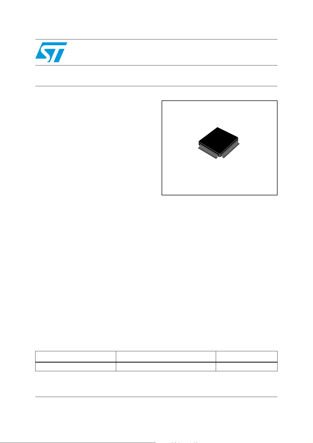
■ TQFP100 exposed pad package
Description
The L9390 is a twelve output low side valve driver
designed for use in an ABS/ESP vehicle system.
All outputs are PWM configurable, while six out of
twelve are current regulated. Each of the twelve
outputs is open drain configured and has a built-in
35V clamp. Eight of the twelve have integrated
Table 1. Device summary
L9390
Twelve channel valve driver
Data Brief
TQFP100
(Exposed pad down)
active freewheeling diodes for active rectification
of the PWM controlled load.
In order to minimize electromagnetic emissions
during load actuation, the possibility to control
output slopes is provided.
Two separate communication interfaces are
present: the SPI port is primarily designated to
provide diagnostics and secondary control. The
serial High End Timer Interface (HET) provides
the primary output control functions from on/off
switching to current level control commands.
Diagnostic includes over current protection, under
current detection, open load detection, loss of
ground detection, loss of freewheeling diode, and
over temperature detection, output integrity
check, SVDT, leakage current test, PWM integrity
and functionality check, valve resistance sense
check, loss of freewheeling diode detection and
more.
Power supply monitoring is also included.
Part number Package Packing
L9390 TQFP100 14x14x1.0mm (exposed pad down) Tray
March 2007 Rev 1 1/8
For further information contact your local STMicroelectronics sales office.
www.st.com
8
Pin description L9390
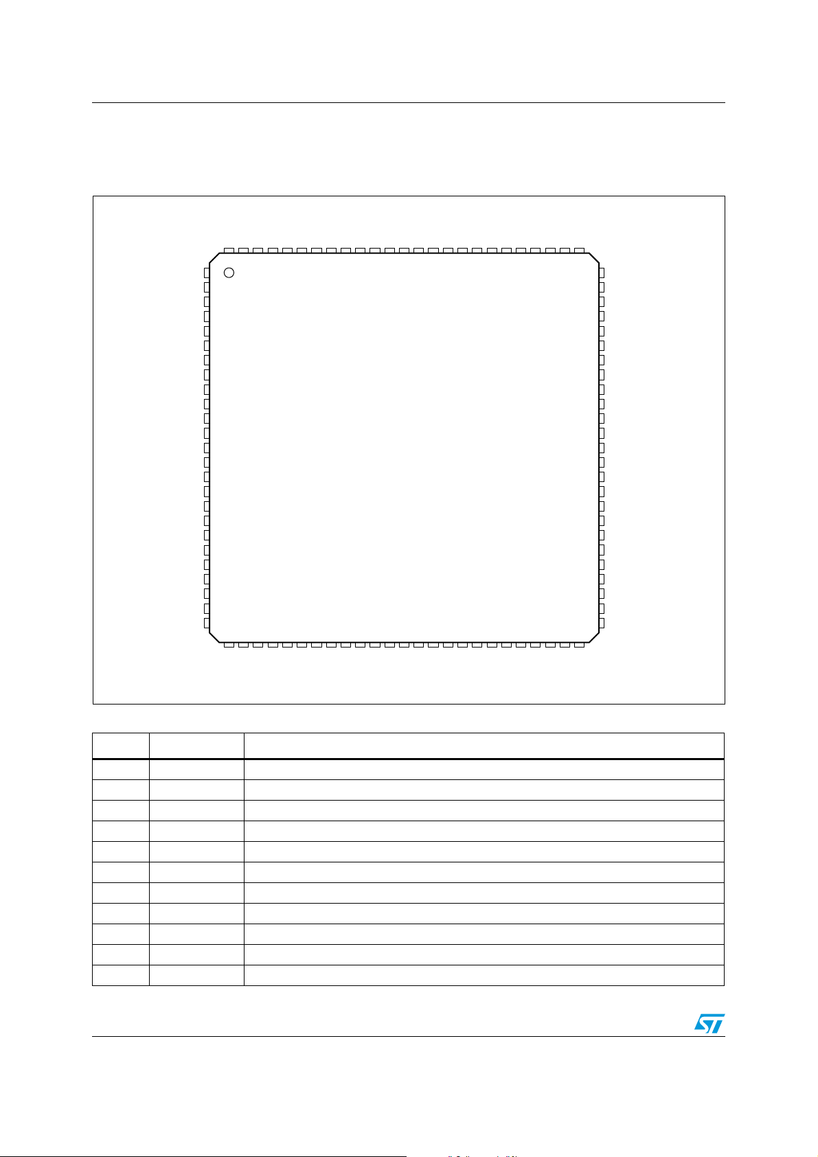
1 Pin description
Figure 1. Pin connection (top view)
OUT7
OUT7
PGND3_7
PGND3_7
PGND3_7
OUT3
PGND3_7
OUT3D8D8
OUT2
OUT2
OUT2
N.C.
PGND2_6
PGND2_6
PGND2_6
PGND2_6
PGND2_6
OUT6
N.C.D7D7
100 99 98
1
2
3
4
5
6
7
8
9
10
97 96 95 949293 91 90 89 88 87
OUT6
12
D6
13
D6
14
OUT1
15
OUT1
OUT5
OUT5
N.C.
16
17
18
19
20
21
22
23
D5
D5
24
25
26 27 28
N.C.
V
29 30 31 32 33
S
N.C.
VCP
HET1-6
HET1-6
HET1-6
HET1-6
34 35 36 37 38 39
V3
HET1-6
HET1-6
PGND1_5
PGND1_5
PGND1_5
PGND1_5
PGND1_5
Table 2. Pins description
Pin # Name Description
OUT8
OUT8
PGND4_8
PGND4_8
PGND4_8
PGND4_8
86 85 84 838182 80 79 78 77 76
40 41 42 43 44
N.C.
LOGI
VRS_Meas
DGND
OUT_EN
AGND
N.C.
CLKin
OUT4
N.C.D9D9
OUT4
451146 47 48 49 50
CS
CLK
MISO
MOSI
BUSY
D9
75
74
73
72
71
70
69
68
67
66
65
64
63
62
61
60
59
58
57
56
55
54
53
52
51
N.C.
OUT9
OUT9
OUT9
OUT9
PGND9
PGND9
PGND9
PGND9
OUT11
OUT11
D11
D11
D10
D10
OUT10
OUT10
PGND10_12
PGND10_12
PGND10_12
PGND10_12
PGND10_12
OUT12
OUT12
D12
D12
AC00078
1-3 OUT2 Valve Low Side Driver output, Switched or PWMmed
4 N.C. Not Connected
5-9 PGND2_6 Dedicated Output Power Ground
10-11 OUT6 Valve Low Side Driver output, PWMmed or Current Regulated
12-13 D6 Freewheeling Diode Cathode
14-15 OUT1 Valve Low Side Driver output, Switched or PWMmed
16-20 PGND1_5 Dedicated Output Power Ground
21-22 OUT5 Valve Low Side Driver output, PWMmed or Current Regulated
23-24 D5 Freewheeling Diode Cathode
25-26 N.C. Not Connected
27 Vs Battery level Supply input voltage
2/8

L9390 Pin description
Table 2. Pins description (continued)
Pin # Name Description
28 VCP Charge Pump voltage input
29 N.C. Not Connected
30-35 HET1-6 Serial High End Timer inputs
36 V3 3.3V supply input
37 LOGI Logic Supply Input, must be tied to V3
38 VRS_Meas Switch connection to pin D5 for the purpose of diagnosing specific load resistances.
39 OUT_EN Enables/ disables all outputs asynchronous to any other commands
40 DGND Circuit ground
41 AGND Signal Ground
42-43 N.C. Not Connected
44 CLKin Clock input for IC
45 CS SPI Chip Select input
46 CLK SPI Clock input
47 MISO SPI Master in Slave out
48 MOSI SPI Master out Slave in
49 BUSY SPI Enable input
50 N.C. Not Connected
51-52 D12 Freewheeling Diode Cathode
53-54 OUT12 Valve Low Side Driver output, Current Regulated
55-59 PGND10_12 Dedicated Output Power Ground
60-61 OUT10 Valve Low Side Driver output, Current Regulated
62-63 D10 Freewheeling Diode Cathode
64-65 D11 Freewheeling Diode Cathode
66-67 OUT11 Valve Low Side Driver output, PWMmed
68-71 PGND9 Dedicated Output Power Ground
72-75 OUT9 Valve Low Side Driver output, PWMmed
76-78 D9 Freewheeling Diode Cathode
79 N.C. Not Connected
80-81 OUT4 Valve Low Side Driver output, Switched or PWMmed
82-85 PGND4_8 Dedicated Output Power Ground
86-87 OUT8 Valve Low Side Driver output, PWMmed or Current Regulated
88-89 D8 Freewheeling Diode Cathode
90-91 OUT3 Valve Low Side Driver output, Switched or PWMmed
92-95 PGND3_7 Dedicated Output Power Ground
96-97 OUT7 Valve Low Side Driver output, PWMmed or Current Regulated
98-99 D7 Freewheeling Diode Cathode
100 N.C. Not Connected
3/8

Block diagram L9390
2 Block diagram
Figure 2. Block diagram
V3
OUT4
PGND4_8
OUT3
PGND3_7
OUT2
PGND2_6
OUT1
PGND1_5
D8
OUT8
PGND4_8
D7
OUT7
PGND3_7
D6
OUT6
PGND2_6
D5
OUT5
PGND1_5
D12
OUT12
PGND10_12
D11
OUT9_11
PGND11
D10
OUT10
PGND10_12
D9
OUT9
PGND9_11
VRS_Meas
VCP
Vs
V3
Logic
CS
CLK
MOSI
MISO
BUSY
CLKin
OUT_EN
HET1
HET2
HET3
HET4
HET5
HET6
DGND
AGND
Power Supply
Monitoring
UV, OV
SPI
Port
CLKin
Monitor
Serial
High
End
Timer
Interface
R
LIMIT
VRS Switch
CONTROL CIRCUIT
Data and Comand Registers
From D5
Valve Driver
Control Ckt
PWM/Switch
Control &
Diagnostics
Valve Driver
Control Ckt
Current Control
Control &
Diagnostics
Valve Driver
Control Ckt
Current Control
Control &
Diagnostics
Valve Driver
Control Ckt
PWM/Control
& Diagnostics
SWITCH/PW M
Output Stage x4 Drivers
SWITCH/PW M
Output Stage w/Diodes x4 Drivers
w/Diodes
x2 Drivers
Output Stage
SWITCH/PW M
w/Diodes
x2 Drivers
Output Stage
SWITCH/PW M
4/8
AC00079

L9390 Electrical specifications
3 Electrical specifications
3.1 Absolute maximum ratings
Warning: The absolute maximum ratings are the values at which if
exceeded the device may become damaged.
Table 3. Absolute maximum ratings
Val ue
PIN/Parameter Name Parameter
Min Max
Supply Voltage (Continuous) -0.3 +20 V
V
S
Supply Voltage (t < 5 min) +27 V
VS, VCP Supply Voltage τ < 400ms +35 V
V3, VLOGIC Maximum Voltage +3.6 V
CS, CLK, MOSI, MISO,
EN, CLKin, HETx
Maximum Voltage -0.3 +3.6 V
OUT_EN Maximum Voltage -0.3 +3.6 V
VRS_Meas Maximum Voltage -0.3 +3.6 V
OUTx, Dx Maximum Voltage -0.3 +35 V
T
J(Operating)
T
J(Operating)
T
J(Storage)
1. Internally limited
2. Allowed only during switch-off
Junction Temperature -40
Junction Temperature (1h over life-time) +190
Storage Temperature -65 +150 °C
(1)
(2)
Unit
°C
°C
3.2 Thermal data
th(j-a)
th(j-c)
Junction Temperature -40 +150 °C
Ambient Temperature -40 +105 °C
Thermal resistance Junction to Ambient
Thermal resistance Junction to case 2 °C/W
Maximum OUTx clamping energy, Single Pulse 50 mJ
Table 4. Thermal data
Symbol Parameter
T
J(Operating)
T
A(Operating)
R
R
E
OUT(MAX)
Val ue
Unit
Min Max
(3)
20 °C/W
5/8

Package information L9390
4 Package information
In order to meet environmental requirements, ST offers these devices in ECOPACK®
packages. These packages have a Lead-free second level interconnect. The category of
second Level Interconnect is marked on the package and on the inner box label, in
compliance with JEDEC Standard JESD97. The maximum ratings related to soldering
conditions are also marked on the inner box label. ECOPACK is an ST trademark.
ECOPACK specifications are available at: www.st.com.
Figure 3. TQFP100 mechanical data & package dimensions
DIM.
A 1.200 0.0472
A1 0.050 0.150 0.0020 0.0059
A2 0.950 1.000 1.050 0.0374 0.0394 0.0413
b 0.170 0.22 0 0.270 0.0067 0.0087 0.0106
c 0.090 0.200 0.0035 0.0079
D 15.800 16.000 16.200 0.6220 0.6299 0.6378
D1 13.800 14 .000 14.200 0.5433 0.5512 0.5591
(1)
D2
D3 12.000 0.4724
E 15.800 16.000 16.200 0.6220 0.6299 0.6378
E1 13.800 14.000 14.20 0 0.5433 0.5512 0.5591
(1)
E2
E3 12.000 0.4724
e 0.500 0.0197
L 0.450 0.60 0 0.750 0.0177 0.0236 0.0295
L1 1.000 0.0394
k 3.500 7.000 0.1378 0.2756
ccc 0.080 0.0031
(1) The size of exposed pad is variable depending of leadframe de-
sign pad size. End user should verify “D2” and “E2” dimensions
for each device application.
mm inch
MIN. TYP. MAX. MIN. TYP. MAX.
2.000 0.0787
2.000 0.0787
OUTLINE AND
MECHANICAL DATA
TQFP100 (14x14x1.40mm)
Exposed pad down
6/8
7357321 C

L9390 Revision history
5 Revision history
Table 5. Document revision history
Date Revision Changes
22-Mar-2007 1 Initial release.
7/8

L9390
Please Read Carefully:
Information in this document is provided solely in connection with ST products. STMicroelectronics NV and its subsidiaries (“ST”) reserve the
right to make changes, corrections, modifications or improvements, to this document, and the products and services described herein at any
time, without notice.
All ST products are sold pursuant to ST’s terms and conditions of sale.
Purchasers are solely responsible for the choice, selection and use of the ST products and services described herein, and ST assumes no
liability whatsoever relating to the choice, selection or use of the ST products and services described herein.
No license, express or implied, by estoppel or otherwise, to any intellectual property rights is granted under this document. If any part of this
document refers to any third party products or services it shall not be deemed a license grant by ST for the use of such third party products
or services, or any intellectual property contained therein or considered as a warranty covering the use in any manner whatsoever of such
third party products or services or any intellectual property contained therein.
UNLESS OTHERWISE SET FORTH IN ST’S TERMS AND CONDITIONS OF SALE ST DISCLAIMS ANY EXPRESS OR IMPLIED
WARRANTY WITH RESPECT TO THE USE AND/OR SALE OF ST PRODUCTS INCLUDING WITHOUT LIMITATION IMPLIED
WARRANTIES OF MERCHANTABILITY, FITNESS FOR A PARTICULAR PURPOSE (AND THEIR EQUIVALENTS UNDER THE LAWS
OF ANY JURISDICTION), OR INFRINGEMENT OF ANY PATENT, COPYRIGHT OR OTHER INTELLECTUAL PROPERTY RIGHT.
UNLESS EXPRESSLY APPROVED IN WRITING BY AN AUTHORIZED ST REPRESENTATIVE, ST PRODUCTS ARE NOT
RECOMMENDED, AUTHORIZED OR WARRANTED FOR USE IN MILITARY, AIR CRAFT, SPACE, LIFE SAVING, OR LIFE SUSTAINING
APPLICATIONS, NOR IN PRODUCTS OR SYSTEMS WHERE FAILURE OR MALFUNCTION MAY RESULT IN PERSONAL INJURY,
DEATH, OR SEVERE PROPERTY OR ENVIRONMENTAL DAMAGE. ST PRODUCTS WHICH ARE NOT SPECIFIED AS "AUTOMOTIVE
GRADE" MAY ONLY BE USED IN AUTOMOTIVE APPLICATIONS AT USER’S OWN RISK.
Resale of ST products with provisions different from the statements and/or technical features set forth in this document shall immediately void
any warranty granted by ST for the ST product or service described herein and shall not create or extend in any manner whatsoever, any
liability of ST.
ST and the ST logo are trademarks or registered trademarks of ST in various countries.
Information in this document supersedes and replaces all information previously supplied.
The ST logo is a registered trademark of STMicroelectronics. All other names are the property of their respective owners.
© 2007 STMicroelectronics - All rights reserved
STMicroelectronics group of companies
Australia - Belgium - Brazil - Canada - China - Czech Republic - Finland - France - Germany - Hong Kong - India - Israel - Italy - Japan -
Malaysia - Malta - Morocco - Singapore - Spain - Sweden - Switzerland - United Kingdom - United States of America
www.st.com
8/8
 Loading...