

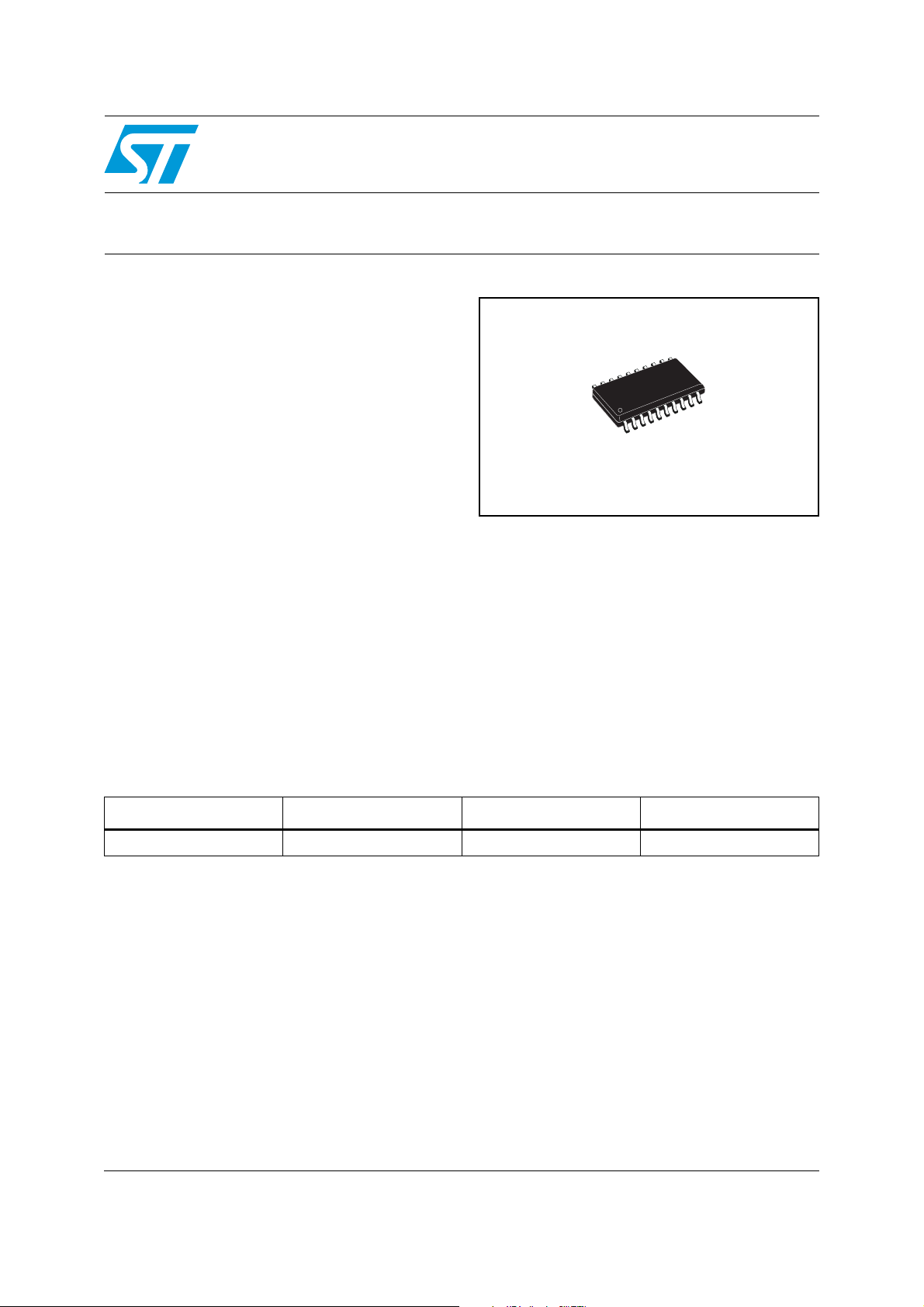
Dual intelligent power low side switch
Features
■ Multipower BCD technology
■ Dual power low side driver with 2 x 5 A
■ Low R
■ Internal output clamping diodes V
inductive recirculation
■ Limited output voltage slew rate for low EMI
■ µP compatible enable and input
■ Wide operating supply voltage range 4.5 V to
45 V
■ Real time diagnostic functions:
– Output shorted to GND
– Output shorted to V
– Open load
– Load bypass
– Over temperature
■ Device protection functions:
– Overload disable
– Reverse battery up to -16 V @ V
– Thermal shutdown
Table 1. Device summary
typically 200 mΩ @ TJ = 25 °C
DSON
SS
= 50 V for
FB
S
L9386
SO20
Description
The L9386 is a monolithic integrated dual low side
driver realized in an advanced Multipower BCD
mixed technology.
It is especially intended to drive valves in
automotive environment. Its inputs are µP
compatible for easy driving. Particular care has
been taken to protect the device against failures,
to avoid electro-magnetic interferences and to
offer extensive real time diagnostic.
Part number Order code Package Packing
L9386 L9386MD SO20 (12+4+4) Tube
July 2008 Rev 3 1/14
www.st.com
14

Contents L9386
Contents
1 Block and pins connection diagrams . . . . . . . . . . . . . . . . . . . . . . . . . . . 3
2 Electrical specifications . . . . . . . . . . . . . . . . . . . . . . . . . . . . . . . . . . . . . . 4
2.1 Absolute maximum ratings . . . . . . . . . . . . . . . . . . . . . . . . . . . . . . . . . . . . . 4
2.2 Thermal data . . . . . . . . . . . . . . . . . . . . . . . . . . . . . . . . . . . . . . . . . . . . . . . 4
2.3 Electrical characteristics . . . . . . . . . . . . . . . . . . . . . . . . . . . . . . . . . . . . . . . 5
2.4 Circuit description . . . . . . . . . . . . . . . . . . . . . . . . . . . . . . . . . . . . . . . . . . . 10
3 Package information . . . . . . . . . . . . . . . . . . . . . . . . . . . . . . . . . . . . . . . . 12
4 Revision history . . . . . . . . . . . . . . . . . . . . . . . . . . . . . . . . . . . . . . . . . . . 13
2/14
L9386 Block and pins connection diagrams
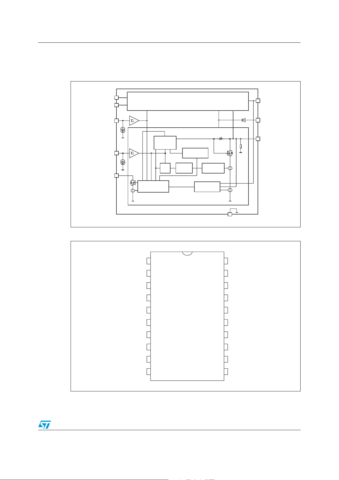
1 Block and pins connection diagrams
Figure 1. Block diagram
IN1
DIAG1
EN
Output
Diagnostic
Control
Control
R
QS
IN2
DIAG2
Channel 2
Figure 2. Pins connection (top view)
Channel 1
Overtemp
Delay
Timer
Overload
Openload
GND
OUT1
VS
OUT2
R
O
IN1
DIAG2
OUT2
GND
GND
GND
GND
N.C.
EN
VS
1
2
3
4
5
6
7
8
9
10
IN2
20
DIAG1
19
OUT1
18
GND
17
GND
16
GND
15
GND
14
13
N.C.
N.C.
12
11
N.C.
3/14
Electrical specifications L9386
2 Electrical specifications
2.1 Absolute maximum ratings
Table 2. Absolute maximum ratings (no damage or latch)
Symbol Parameter Value Unit
V
DC supply voltage -16 to 45 V
SDC
Transient supply voltage (t ≤ 500 ms) 60 V
V
STR
,EN Input voltage (| ≤ | 10 mA |) -1.5 to 6 V
V
IN
V
Diagnostic DC output voltage (| ≤ | 50 mA |) -0.3 to 16 V
DDC
DC output voltage 45 V
V
ODC
Transient output voltage (RL ≥ 4 Ω) 60 V
V
OTR
I
Output load current internal limited
O
Reverse output current limited by load -4 A
I
OR
EO
T
jEO
T
T
stg
Switch-off energy for inductive loads
(t
= 250 µs, T = 5 ms)
EO
50 mJ
Junction temperature during switch-off Σt = 30 min 175 °C
Junction temperature -40 to +150 °C
j
Storage temperature -55 to +150 °C
2.2 Thermal data
Table 3. Thermal data
Symbol Parameter Value Unit
T
Thermal disable junction temperature threshold 160 to 190 °C
jDIS
R
Thermal resistance junction to pins 14 °C/W
th j-pins
4/14
L9386 Electrical specifications
2.3 Electrical characteristics
Table 4. Electrical characteristics
(The electrical characteristics are valid within the below defined operative range, unless
otherwise specified.)
Symbol Parameter Test condition Min. Typ. Max. Unit
V
V
T
IS
SB
IS DC supply current
VD
ID
LE
ID
VO
ΔVO
UV1,2
IO
UC
IO
OC
V
OCL
S
ON,OFF
R
IO
R
DSON
Board supply voltage 4.5 12 32 V
S
Stabilized diagnostic output
D
voltage
Junction temperature -40 150 °C
j
(1)
Static standby supply current
Diagnostic output low voltage
L
Diagnostic output leakage
current
Diagnostic output current
capability
Open load voltage threshold VEN = X, VIN = L
UV
Open load difference voltage
threshold
Open load current threshold
(2)
VEN = L, VO ≤ VOuv
(1)
(2)
VEN = VIN = H
(1)
ID = 2 mA
(2)
ID = 1 mA
= 0 V or VS = open;
V
S
= 5.5 V Tj ≤ 125 °C
V
D
VD ≤ 16 V DIAG = L 2 6 30
(1)
VEN = X, V
≥ VOC ≥ VOUV
V
S
= output voltage of other
VO
C
IN1,2
= L
channel
(2)
(3)
VEN = VIN = H
(2)
-0.3 5 16 V
0.73 1.5
1.3
0.35 0.5 V
0.1 2 mA
0.51
xVS
VO
0.9V
VO
0.7V
100
-
C
-
C
0.55
xVS
-
VO
C
1.25V
VO
-
C
1.25V
320 480
20
Over load current threshold b) 5 7 A
Output voltage during clamping IOCL ≥ 100mA 45 52 60 V
Output (fall, rise) slew rate
Internal output pull down
resistor
Output on resistance
(3)
see Figure 4 200 1500 3200 V/ms
= L 10 20 40 KΩ
V
EN
V
> 9.5 V IO = 2 A
S
= 25 °C
T
j
200 300
Tj = 150 °C
15
5
15
0.59
xVS
VO
1.6V
VO
1.8V
500
mA
mA
mA
V
-
C
V
-
C
mA
mΩ
V
(EN,IN)L
V
(EN,IN)H
|IEN, IN| ≤ 10 mA
Logic input low voltage
(1)
(2)
-1.5
-1.5
1
0.5
Logic input high voltage 2.2 5.5 V
5/14
V

Electrical specifications L9386
Table 4. Electrical characteristics (continued)
(The electrical characteristics are valid within the below defined operative range, unless
otherwise specified.)
Symbol Parameter Test condition Min. Typ. Max. Unit
V
(EN,IN)hys
I
EN
I
IN
t
DON
t
DOFF
t
DH-L,Diag.
t
DIOu
t
DOL
1. 6.5 V ≤ VS ≤ 16 V (Diagnostic operation range).
2. 4.5 V ≤ V
3. 9 V ≤ V
RL ≤ 6 Ω, IO ≤ IO
Table 5. Diagnostic table (operating range: 4.5 V ≤ VS ≤ 32 V)
Logic input hysteresis 0.2 0.4 1 V
Enable input sink current 1 V ≤ VEN ≤ 5.5 V 10 30 60 µA
Logic input sink current 1 V ≤ VIN ≤ 5.5 V 40 95 180 µA
Output delay ON time
Output delay OFF time
Diag. delay output OFF time
Diagnostic open load delay time
Diagnostic overload delay
switch-off time
< 6.5 V and 16 V < VS ≤ 32 V (Extended operation range).
S
≤ 16 V (Nominal operating range)
S
OC.
(3)
see Figure 4 425µs
(3)
see Figure 4 51530µs
(3)
see Figure 4 53065µs
(3)
see Figure 6 850µs
(3)
see Figure 3 50 160 300 µs
Conditions EN IN Out Diag.
Normal function
GND short VO
Load bypass ΔVO
Open load IO
T
≥ 175 °C overtemperature
j typ
L
H
H
< 0.55 V
typ
≥ 1.25 V
1,2
< 320 mA H H on
typ
(2)
L
H
X
X
X
L
H
X
L
L
H
off
off
(1)
on
off
off
(1)
L
off
off
L
L
H
H
H
H
L
Latched overload IO
Reset overload latch X
1. for 4.5 V ≤ VS < 6.5 V, IO ≤ 2 A diag. table is valid.
2. If one diag. status shows the overtemperature recognition, in parallel this output will be switched OFF internally. The
corresponding channel should be switched OFF additional by its Input or ENABLE signal, otherwise the overload latch will
be set after t
recognition.
is passed. This behavior will be related to the overdrop sensing which will be used as over load
DOL
> 5 A X H off L
min
D.C. D.C.
6/14

L9386 Electrical specifications
Figure 3. Diagnostic overload delay time
UI
5V
t
IO
IO
SC
5A
IO
UC
td
OL
UD
5V
t
Figure 4. Output slope
U
IN
5V
V
(IN)H
V
(IN)L
U
OUT
VO
C
0.85VO
C
VS
VS-VO
CC
0.85VS
VO
UV
0.15VS
V
DIAG
V
D
0.5V
D
t
td
on
S
on
td
off
S
off
t
t
t
D
H-L
Diag
t
7/14

Electrical specifications L9386
Figure 5. Open load voltage detection block diagram
V
Batt.
L1 L2
OUT1 OUT2
IN
1
VS
55%
Enable
R
IO
R
IO
+
-
+
-
IN
2
& &
R
S
Latch
Latch
S
Q
R
Q
& &
8/14
VO
UV1
VO
UV2

L9386 Electrical specifications
Figure 6. Logic diagram
open load
voltage
normal
operation
OFF
ON
latch reset
open load voltage
open load current
off
td
normal
operation
u
on
td
IO
td
latched over.
load diagnostic
OL
td
over load
current
open load
current
normal
operation
u
on
td
IO
td
open load current
normal
operation
OFF ON
EN
V
IN
V
u
VO
o
IO
IO
u
D
V
9/14

Electrical specifications L9386
2.4 Circuit description
The L9386 is a dual low side driver for inductive loads like valves in automotive environment.
The device is enabled by a common CMOS compatible ENABLE high signal. The internal
pull down current sources at the ENABLE and INPUT pins protect the device in open input
conditions against malfunctions. An output slope limitation for du/dt is implemented to
reduce the EMI. An integrated active flyback voltage limitation clamps the output voltage
during the flyback phase to 50V.
Each driver is protected against short circuit and thermal overload. In short circuit condition
the output will be disabled after a short delay time t
latched until a negative slope occur at the correspondent input pin. The thermal disable for
T
> 175 °C of the output will be resetted if the junction temperature decreases about 20 °C
J
below the disable threshold temperature.
For the real time error diagnosis the voltage and the current of the outputs are compared
with internal fixed values V
(R
≥ 20 kΩ, RL > 38Ω) in ON and OFF conditions. The diagnostic operates also in the
L
extended supply voltage range of 4.5 V ≤ V
Also the output voltages VO
fixed offset of ΔVO
UV 1,2
for OFF and I
OUV
are compared against each other in OFF condition with a
1,2
OUC
≤ 32 V.
S
to recognize GND bypasses. To suppress mail ΔVO diagnoses
during the flyback phases of the compared output, the ΔVO diagnostic
to suppress spikes. This disable is
DOL
for ON conditions to recognize open load
includes a latch function. Reaching the flyback clamping voltage VO
the diagnostic signal
C
is resetted by a latch. To activate again this kind of diagnostic a low signal at the
correspondent INPUT or the ENABLE pin must occur (see also Figure 5).
The diagnostic output level in connection with different ENABLE and INPUT conditions
allows to recognize different fail states, like overtemperature, short to VSS, short to GND,
bypass to GND and disconnected load (see also Table 5 on page 6).
The diagnostic output is also protected against short to UD
current threshold IO
overload delay switch-off time t
, the output current will be limited internally during the diagnostic
o
DOL
.
. Oversteping the over load
max
10/14

L9386 Electrical specifications
Figure 7. Open load voltage detection block diagram
+5V
µ P
Controller
IN1
DIAG1
EN
IN2
DIAG2
Diagnostic
Control
Output
Control
R
QS
Channel 1
Overtemp
Delay
Timer
Channel 2
Overload
Openload
GND
Z
VALVE
OUT1
VS
OUT2
R
O
Z
VALVE
V
Batt
11/14

Package information L9386
3 Package information
In order to meet environmental requirements, ST (also) offers these devices in ECOPACK®
packages. ECOPACK
®
packages are lead-free. The category of second Level Interconnect
is marked on the package and on the inner box label, in compliance with JEDEC Standard
JESD97. The maximum ratings related to soldering conditions are also marked on the inner
box label.
ECOPACK is an ST trademark. ECOPACK specifications are available at: www.st.com.
Figure 8. SO20 mechanical data and package dimensions
DIM.
A 2.35 2.65 0.093 0.104
A1 0.10 0.30 0.004 0.012
B 0.33 0.51 0.013 0.200
C 0.23 0.32 0.009 0.013
(1)
D
E 7.40 7.60 0.291 0.299
e 1.27 0.050
H 10.0 10.65 0.394 0.419
h 0 .25 0.75 0.010 0.0 30
L 0 .40 1.27 0.016 0.0 50
k 0˚ (min.), 8˚ (max.)
ddd 0.10 0.004
(1) “D” dimensio n does not include mold flash, prot usions or gate
burrs. Mol d flash, protus ions or gat e burrs shall no t exceed
0.15mm per sid e.
mm inch
MIN. TYP. MAX. MIN. TYP. MAX.
12.60 13.00 0.496 0.512
OUTLINE AND
MECHANICAL DATA
SO20
12/14
0016022 D

L9386 Revision history
4 Revision history
Table 6. Document revision history
Date Revision Changes
16-Jan-2002 1 Initial release.
20-Sep-2003 2 Changed company name and logo.
16-Jul-2008 3
Document reformatted.
Added Table 1: Device summary on page 1.
13/14

L9386
Please Read Carefully:
Information in this document is provided solely in connection with ST products. STMicroelectronics NV and its subsidiaries (“ST”) reserve the
right to make changes, corrections, modifications or improvements, to this document, and the products and services described herein at any
time, without notice.
All ST products are sold pursuant to ST’s terms and conditions of sale.
Purchasers are solely responsible for the choice, selection and use of the ST products and services described herein, and ST assumes no
liability whatsoever relating to the choice, selection or use of the ST products and services described herein.
No license, express or implied, by estoppel or otherwise, to any intellectual property rights is granted under this document. If any part of this
document refers to any third party products or services it shall not be deemed a license grant by ST for the use of such third party products
or services, or any intellectual property contained therein or considered as a warranty covering the use in any manner whatsoever of such
third party products or services or any intellectual property contained therein.
UNLESS OTHERWISE SET FORTH IN ST’S TERMS AND CONDITIONS OF SALE ST DISCLAIMS ANY EXPRESS OR IMPLIED
WARRANTY WITH RESPECT TO THE USE AND/OR SALE OF ST PRODUCTS INCLUDING WITHOUT LIMITATION IMPLIED
WARRANTIES OF MERCHANTABILITY, FITNESS FOR A PARTICULAR PURPOSE (AND THEIR EQUIVALENTS UNDER THE LAWS
OF ANY JURISDICTION), OR INFRINGEMENT OF ANY PATENT, COPYRIGHT OR OTHER INTELLECTUAL PROPERTY RIGHT.
UNLESS EXPRESSLY APPROVED IN WRITING BY AN AUTHORIZED ST REPRESENTATIVE, ST PRODUCTS ARE NOT
RECOMMENDED, AUTHORIZED OR WARRANTED FOR USE IN MILITARY, AIR CRAFT, SPACE, LIFE SAVING, OR LIFE SUSTAINING
APPLICATIONS, NOR IN PRODUCTS OR SYSTEMS WHERE FAILURE OR MALFUNCTION MAY RESULT IN PERSONAL INJURY,
DEATH, OR SEVERE PROPERTY OR ENVIRONMENTAL DAMAGE. ST PRODUCTS WHICH ARE NOT SPECIFIED AS "AUTOMOTIVE
GRADE" MAY ONLY BE USED IN AUTOMOTIVE APPLICATIONS AT USER’S OWN RISK.
Resale of ST products with provisions different from the statements and/or technical features set forth in this document shall immediately void
any warranty granted by ST for the ST product or service described herein and shall not create or extend in any manner whatsoever, any
liability of ST.
ST and the ST logo are trademarks or registered trademarks of ST in various countries.
Information in this document supersedes and replaces all information previously supplied.
The ST logo is a registered trademark of STMicroelectronics. All other names are the property of their respective owners.
© 2008 STMicroelectronics - All rights reserved
STMicroelectronics group of companies
Australia - Belgium - Brazil - Canada - China - Czech Republic - Finland - France - Germany - Hong Kong - India - Israel - Italy - Japan -
Malaysia - Malta - Morocco - Singapore - Spain - Sweden - Switzerland - United Kingdom - United States of America
www.st.com
14/14
 Loading...