

Page 1
Features
■ Overvoltage charge pump shut off
■ For V
■ Reverse battery protection (referring to the
> 25 V
S
application circuit diagram)
■ Programmable overload protection function for
channel 1 and 2
■ Open ground protection function for channel 1
and 2
■ Constant gate charge/discharge current
Description
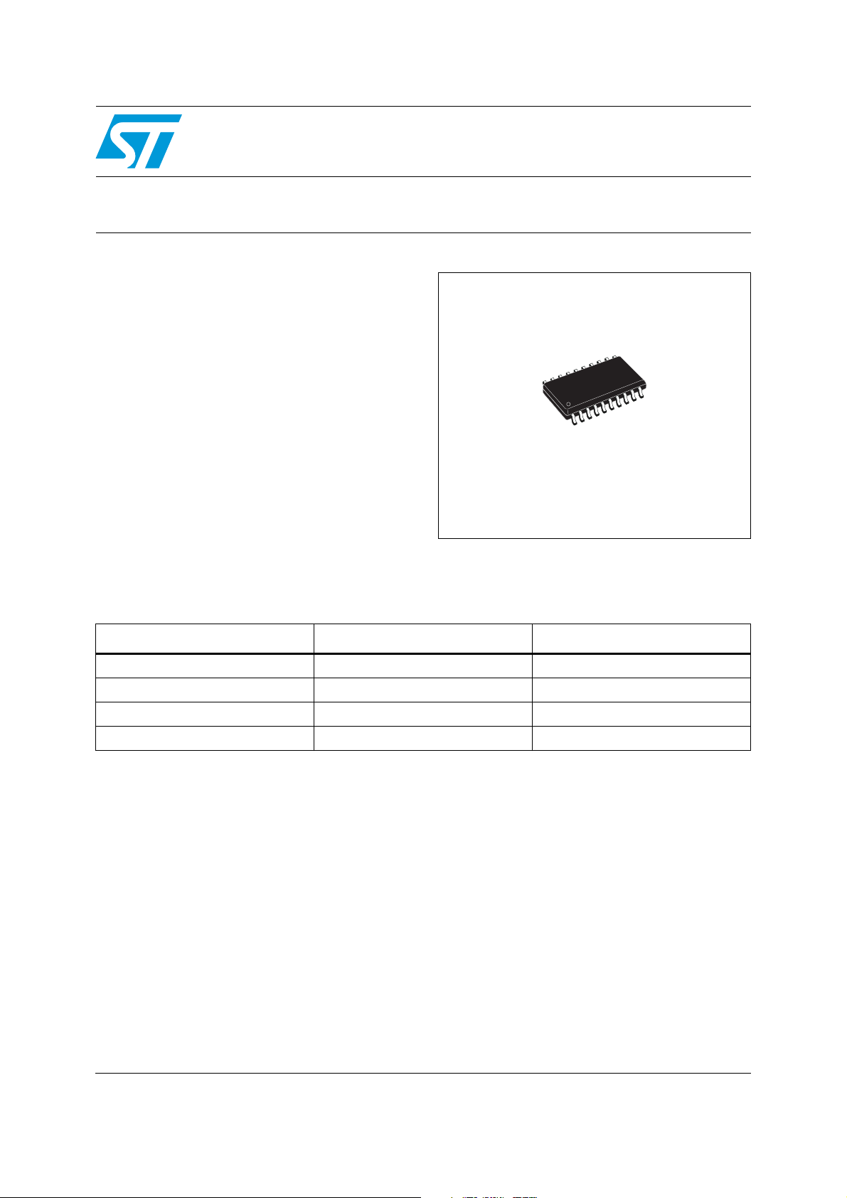
L9380
Triple high-side MOSFET driver
SO20
The L9380 device is a controller for three external
N-channel power MOS transistors in "High-Side
Switch" configuration.
Table 1. Device summary
Order code Package Packing
L9380 SO20 Tube
L9380-TR SO20 Tape and reel
L9380-LF
L9380-TR-LF
1. Devices in ECOPACK® packages (see Section 5: Package information on page 16).
(1)
(1)
It is intended for relays replacement in automotive
electric control units.
SO20 Tube
SO20 Tape and reel
February 2010 Doc ID 5853 Rev 3 1/18
www.st.com
1
Page 2

Contents L9380
Contents
1 Block diagram . . . . . . . . . . . . . . . . . . . . . . . . . . . . . . . . . . . . . . . . . . . . . . 5
2 Pins description . . . . . . . . . . . . . . . . . . . . . . . . . . . . . . . . . . . . . . . . . . . . 6
3 Electrical specifications . . . . . . . . . . . . . . . . . . . . . . . . . . . . . . . . . . . . . . 7
3.1 Absolute maximum ratings . . . . . . . . . . . . . . . . . . . . . . . . . . . . . . . . . . . . . 7
3.2 Thermal data . . . . . . . . . . . . . . . . . . . . . . . . . . . . . . . . . . . . . . . . . . . . . . . 7
3.3 Electrical characteristics . . . . . . . . . . . . . . . . . . . . . . . . . . . . . . . . . . . . . . . 7
4 Functional description . . . . . . . . . . . . . . . . . . . . . . . . . . . . . . . . . . . . . . . 9
4.1 Typical characteristics curve . . . . . . . . . . . . . . . . . . . . . . . . . . . . . . . . . . . 13
4.1.1 Electromagnetic emission classification (EME) . . . . . . . . . . . . . . . . . . . 15
5 Package information . . . . . . . . . . . . . . . . . . . . . . . . . . . . . . . . . . . . . . . . 16
6 Revision history . . . . . . . . . . . . . . . . . . . . . . . . . . . . . . . . . . . . . . . . . . . 17
2/18 Doc ID 5853 Rev 3
Page 3

L9380 List of tables
List of tables
Table 1. Device summary . . . . . . . . . . . . . . . . . . . . . . . . . . . . . . . . . . . . . . . . . . . . . . . . . . . . . . . . . . 1
Table 2. Pins function . . . . . . . . . . . . . . . . . . . . . . . . . . . . . . . . . . . . . . . . . . . . . . . . . . . . . . . . . . . . . 6
Table 3. Absolute maximum ratings . . . . . . . . . . . . . . . . . . . . . . . . . . . . . . . . . . . . . . . . . . . . . . . . . . 7
Table 4. Thermal data. . . . . . . . . . . . . . . . . . . . . . . . . . . . . . . . . . . . . . . . . . . . . . . . . . . . . . . . . . . . . 7
Table 5. Electrical characteristics . . . . . . . . . . . . . . . . . . . . . . . . . . . . . . . . . . . . . . . . . . . . . . . . . . . . 7
Table 6. Electromagnetic emission classification . . . . . . . . . . . . . . . . . . . . . . . . . . . . . . . . . . . . . . . 15
Table 7. Document revision history . . . . . . . . . . . . . . . . . . . . . . . . . . . . . . . . . . . . . . . . . . . . . . . . . 17
Doc ID 5853 Rev 3 3/18
Page 4

List of figures L9380
List of figures
Figure 1. Block diagram . . . . . . . . . . . . . . . . . . . . . . . . . . . . . . . . . . . . . . . . . . . . . . . . . . . . . . . . . . . . 5
Figure 2. Pins connection (top view) . . . . . . . . . . . . . . . . . . . . . . . . . . . . . . . . . . . . . . . . . . . . . . . . . . 6
Figure 3. Timing characteristic . . . . . . . . . . . . . . . . . . . . . . . . . . . . . . . . . . . . . . . . . . . . . . . . . . . . . . 10
Figure 4. Drain, source input current. . . . . . . . . . . . . . . . . . . . . . . . . . . . . . . . . . . . . . . . . . . . . . . . . 10
Figure 5. Comparator hysteresis . . . . . . . . . . . . . . . . . . . . . . . . . . . . . . . . . . . . . . . . . . . . . . . . . . . . 11
Figure 6. Application circuit . . . . . . . . . . . . . . . . . . . . . . . . . . . . . . . . . . . . . . . . . . . . . . . . . . . . . . . . 12
Figure 7. Charge loading time as function of VS (Vcp = 8 V +VS) . . . . . . . . . . . . . . . . . . . . . . . . . . 13
Figure 8. Charge pump current as function of the charge voltage. . . . . . . . . . . . . . . . . . . . . . . . . . . 13
Figure 9. Ground loss protection gate discarge current for source voltage . . . . . . . . . . . . . . . . . . . . 13
Figure 10. Input current as function of the input voltage . . . . . . . . . . . . . . . . . . . . . . . . . . . . . . . . . . . 13
Figure 11. Overvoltage shutdown of the charge pump with hysteresis . . . . . . . . . . . . . . . . . . . . . . . . 13
Figure 12. Measured circuit (The EMS of the device was verified in the below described setup) . . . . 14
Figure 13. Printed circuit board (PCB) . . . . . . . . . . . . . . . . . . . . . . . . . . . . . . . . . . . . . . . . . . . . . . . . . 15
Figure 14. SO20 mechanical data and package dimensions. . . . . . . . . . . . . . . . . . . . . . . . . . . . . . . . 16
4/18 Doc ID 5853 Rev 3
Page 5
L9380 Block diagram
1 Block diagram
Figure 1. Block diagram
VS
T1
IN1
T2
IN2
IN3
VSI
VSI
VSI
VSI
DRIVER 1
VSI
DRIVER 2
DRIVER 3
ENN
ENN
ENN
CHARGE PUMP
OVERVOLTAGE
≥1
≥1
-
+
CP
≥1
-
+
CP
≥1
CP
≥1
IPR
IPR
CP
GND
D1
S1
G1
D2
S2
G2
G3
EN
VS VSI
ENN
REFERENCE
REG.
2V
I
PR
PR
D98AT390
Doc ID 5853 Rev 3 5/18
Page 6
Pins description L9380
2 Pins description
Figure 2. Pins connection (top view)
Table 2. Pins function
N°
1T1
2V
4T2
5PR
Pin
name
S
Timer capacitor; the capacitor defines the time for the channel 1 shut down, after overload of
the external MOS transistor has been detected.
Supply voltage.
Timer capacitor; the capacitor defines the time for the channel 2 shut down, after overload of
the external MOS transistor has been detected.
Programming resistor for overload detetcion threshold; the resistor from this pin to ground
defines the drain pin current and the charging of the timer capacitor.
T1
VS
N.C.
T2
PR
IN3
IN2
IN1
EN G2
GND G3
2
3
4
5
6
7
8
9
10
D98AT391
20
19
18
17
16
15
14
13
12
11
Function
6 IN3 Input 3; equal to IN1.
7 IN2 Input 2; equal to IN1.
8IN1
Input 1; logic signal applied to this pin controls the driver 1; this pin features a current source
to assure defined high status when the pin is open.
9 EN Enable logic signal high on this pin enables all channels
10 GND Ground
11 G3 Gate 3 driver output; current source from CP or ground
12 G2 Gate 2 driver output; current source from CP or ground
14 S2 Source 2 sense input; monitors the source voltage.
15 S1 Source 1 sense input; monitors the source voltage.
16 G1 Gate 1 driver output; current source from CP or ground
17 D2
19 D1
Drain 2 sense input; a programmable input bias current defines the drop across the external
resistor R
; this drop fixes the overload threshold of the external MOS.
D1
Drain 1 sense input; a programmable input bias current defines the drop across the external
resistor R
; this drop fixes the overload threshold of the external MOS.
D1
Charge pump capacitor; a alternating current source at this pin charges the connected
20 CP
capacitor C
to a voltage 10V higher than VS; the charge stored in this capacitor is than used
CP
to charge all the three gates of the power MOS transistors.
3, 13, 18 NC Not connected
CP1
D1
N.C.
D2
G1
S1
S2
N.C.
6/18 Doc ID 5853 Rev 3
Page 7

L9380 Electrical specifications
3 Electrical specifications
3.1 Absolute maximum ratings
Table 3. Absolute maximum ratings
Symbol Parameter Value Unit
V
V
ΔV
V
IN,EN
V
V
D, G, S
V
D, G, S
I
D, G, S
T
DC supply voltage -0.3 to +27 V
S
Supply voltage pulse (t ≤ 400 ms) 45 V
S
/dt Supply voltage slope -10 to +10 V/µs
S
Input / enable voltage -0.3 to +7 V
Timer voltage -0.3 to 27 V
T
Drain, gate, source voltage -15 to +27 V
Drain, gate, source voltage pulse (t ≤ 400 ms) 45 V
Drain, gate, source current (t ≤ 2 ms) 0 to +4 mA
T
Operating junction temperature -40 to 150 °C
j
Storage temperature -65 to 150 °C
stg
Note: ESD for all pins, except the timer pins, are according to MIL 883C, tested at 2 kV,
corresponds to a maximum energy dissipation of 0.2 mJ.
The timer pins are tested with 800 V.
3.2 Thermal data
Table 4. Thermal data
Symbol Parameter Value Unit
R
th j-amb
Thermal resistance junction-to-ambient 100 °C/W
3.3 Electrical characteristics
7V ≤ VS ≤ 18.5 V; -40° C ≤ TJ ≤ 150 °C, unless otherwise specified.
Table 5. Electrical characteristics
Symbol Parameter Test condition Min. Typ. Max. Unit
Supply
I
VS
Charge pump
V
CP
I
CP
Static operating supply current VS = 14 V - - 2.5 mA
Charge pump voltage above VS-8-17V
V
= 7 V, VCP = 15 V, Tj ≥ 25 °C -23 - -12 µA
Charge pump current
S
= 7 V, VCP = 15 V, Tj < 25 °C -23 - -10 µA
V
S
Doc ID 5853 Rev 3 7/18
Page 8

Electrical specifications L9380
Table 5. Electrical characteristics (continued)
Symbol Parameter Test condition Min. Typ. Max. Unit
V
= 12 V, VCP = 20 V, Tj ≥ 25 °C -70 - -45 µA
I
t
V
SCP off
V
SCP hys
f
Charge pump current
CP
Charging time VCP = VS + 8 V CCP = 100 pF - - 200 µs
CP
Overvoltage shut down - 20 - 30 V
Overvoltage shut down hysteresis
Charge pump frequency
CP
Gate drivers
(1)
S
= 12 V, VCP = 20 V, Tj < 25 °C -70 - -38 µA
V
S
(1)
- 50 200 1000 mV
- 100 250 400 KHz
I
GSo
I
I
GCP
Gate source current VG = V
Gate sink current VG ≥ 0.8 V 1 3 5 mA
GSi
Charge pump current on the gate
Drain - source sensing
V
I
D Leak
I
Smax
V
HYST
Bias current programming voltage
PR
Drain pin leakage current VS = 0 V; VD =14 V 0 - 5 A
I
Drain pin bias current V
D
Source pin input current V
Comparator hysteresis - - 20 - mV
Timer
V
V
Timer threshold high - 4 4.4 4.8 V
THi
Timer threshold low - 0.3 0.4 0.5 V
TLo
I
Timer current
T
Inputs
V
V
HIGH
V
INhys
I
1. Not measured guaranteed by design.
Input enable low voltage - -0.3 - 1 V
LOW
Input enable high voltage - 3 - 7 V
Input enable hysteresis
I
Input source current VIN ≤ 3 V -30 - -5 μA
IN
Enable sink current VEN ≥ 1 V 5 - 30 μA
EN
Transfer time IN/ENABLE VS = 14 V VG = VS; Open Gate - - 2.5 µs
t
d
(1)
S
-5 -3 -1 mA
VS = 12 V, VG = 20 V, Tj ≥ 25 °C -60 - -35 µA
= 12V, VG = 20 V, Tj < 25 °C -60 - -28 µA
V
S
10 µA ≤ IPR ≤ 100 µA; VD ≥ 4 V 1.822.2V
≥ V
+ 1 V; V
S
D
≥ V
+ 1 V; V
S
D
IN = 5 V; V
IN = 0 V; V
V
≥ 5 V; VT = 2 V
D
≥ 5 V 0.9 I
D
≥ 7 V 10 - 60 A
D
= 2 V
T
< VD;
S
0.4 I
-0.6
I
PR
PR
PR
- 1.1 I
-
0.6 I
-0.4
I
PR
PR
-
PR
- 50 200 500 mV
Function is given for supply voltage down to 5.5 V.
Function means: the channels are controlled from the inputs, some other parameters may
exceed the limit. In this case the programming voltage and timer threshold will be lower. This
leads to a lower protection threshold and time.
8/18 Doc ID 5853 Rev 3
Page 9

L9380 Functional description
4 Functional description
The triple high-side Power-MOS Driver features all necessary control and protection
functions to switch on three Power-MOS transistors operating as High-Side switches in
automotive electronic control units. The key application field is relays replacement in
systems where high current loads, usually motors with nominal currents of about 40 A
connected to ground, has to be switched.
A high signal at the EN pin enables all three channels. With enable low gates are clamped to
ground. In this condition the gate sink current is higher than the specified 3 mA. An enable
low signal makes also a reset of the timer.
A low signal at the inputs switch on the gates of the external MOS. A short circuit at the input
leads to permanent activation of the concerned channel. In this case the device can be
disabled with the enable pin. The charge pump loading is not influenced due to the enable
input.
An external N-channel MOS driver in high side configuration needs a gate driving voltage
higher than V
capacitors and one external charge storage capacitor C
The charge pump is dimensioned to load a capacitor CCP of 33 nF in less than 20 ms up to
8V above V
the decay of the charge pump voltage down to that value where no significant influence on
the application occurs.
. It is generated by means of a charge pump with integrated charge transfer
S
. The value of CCP depends on the input capacitance of the external MOS and
S
CP
.
The necessary charging time for C
has to be respected in the sequence of the input
CP
control signals.
As a consequence the lower gate to source voltage can cause a higher drop across the
Power-MOS and get into overload condition. In this case the overload protection timer will
start.
After the protection time the concerned channel will be switched off. Channel 3 is not
equipped with an overload protection. The same situation can occur due to a discharge of
the storage capacitor caused by the gate short to ground. The gate driver that is supplied
from the pin CP, which is the charge pump output, has a sink and source current capability
of 3 mA. For a short-circuit of the load (source to ground) the L9380 has no gate to source
limitation. The gate source protection must be done externally.
Channel 1 and 2 provide drain to source voltage sensing possibility with programmable
shut-off delay when the activation threshold was exceeded.
This threshold V
resistor is determined by the programming resistor R
also the charge and discharge current of the timer capacitor C
threshold V
DSmin
is set by the external resistor RD. The bias current flowing through this
DSmin
and the timer shut off delay time T
V
DSmin
T
off
V
=
PR
= 4.4 CT R
. This external resistor RPR defines
PR
can be calculated:
o
ff
R
⎛⎞
D
----------- -
⎜⎟
R
⎝⎠
PR
PR
. The drain to source
CT
Doc ID 5853 Rev 3 9/18
Page 10

Functional description L9380
In application which don’t use the overload protection or if one channel is not used, the
Timer pin of this channel must be connected to ground and the drain pin with a resistor to
V
.
bat
The timing characteristic illustrates the function and the meaning of V
Figure 6). The input current of the overload sense comparator is specified as I
I
PR
+ I
generates a drop across the external resistor RD if the drain pin voltage is higher
Dmax
DSmin
and T
Smax
(see
off
. The sum
than the source pin (see Figure 4). In the switching point the comparator input source pin
currents are equal and the half of the specified current I
. For an offset compensation
Smax
equal external resistors (RD = RS) at drain and source pin are imperative. The drain sense
comparator, which detects the overload, has a symmetrical hysteresis of 20 mV (see
Figure 5).
Exceeding the source pin voltage by 10 mV with respect to the drain voltage forces the timer
capacitor to discharge. Decreasing the source pin voltage 10 mV lower than the drain pin
voltage an overload of the external MOS is detected and the timer capacitor will be loaded.
After reaching a voltage at pin CT higher than the timer threshold V
the influenced
Thi
channel is switched off. In this case the overload is stored in the timer capacitor.
The timer capacitor will be discharged with a ’High’ signal at the input (see Figure 3). After
reaching the lower timer threshold V
the overload protection is reset and the channel is
TLo
able to switch on again.
Figure 3. Timing characteristic
V
IN
V
G
t
d
V
S
V
T
4.4V
0.4V
Figure 4. Drain, source input current.
I
D
IPR + I
Dmax
t
d
V
D
> V
V
DSmin
T
off
= V
S
V
S
V
S
> V
D98AT392
D
D
I
PR
0
10/18 Doc ID 5853 Rev 3
D98AT393
I
SmaxIS
Page 11

L9380 Functional description
Figure 5. Comparator hysteresis
V
T
D98AT394
-10mV
+10mV
V
Dr
V
So
The application diagram is shown in Figure 6. Because of the transients present at the
power lines during operation and possible disturbances in the system the external resistors
are necessary.
Positive ISO-Pulses at Drain, Gate Source are clamped with an active clamping structure.
The clamping voltage is less than 60V. Negative Pulses are only clamped with the ESDStructure less than -15 V. This transients lower than -15 V can influence the other channels.
In order to protect the transistor against overload and gate breakdown protection diodes
between gate and source and gate and drain has to be connected. In case of overvoltage
into V
Then the charge pump capacitor will be loaded by a diode and a resistor in series up to V
(VS > 20 V) the charge pump oscillation is stopped.
S
S
(see Figure 1). In this case the channels are not influenced. In reverse battery condition the
pins D1, D2, S1, S2 follow the battery potential down to -13 V (high impedance) and the
gate driver pins G1, G2 is referred to S1, S2. In this way it is assured that M1 and M2 will not
be driven into the linear conductive mode. This protection function is operating for V
S1
, VS2
down to -15 V. The gate driver output G3 is referred to the D1 in this case. This function
guarantees that the source to source connected N-Channel MOS transistors M3 and M4
remains OFF.
All the supplies and the in- and output of the PC Board are supplied with a 40 wires flat
cable (not used wires are left open). This cable is submitted to the RF in the strip-line like
described in DIN 40839-4 or ISO 11456-5.
The measured circuit was build up on a PCB board with ground plane. In the frequency
range from 1 MHz to 400 MHz and 80 % AM-modulation of 1 kHz with field strength of
200 V/m no influence to the basic function was detected on a typical device.
The failure criteria is an envelope of the output signal with 20 % in the amplitude and 2 % in
the time.
Doc ID 5853 Rev 3 11/18
Page 12

Functional description L9380
Figure 6. Application circuit
D1
V
BAT
MICROCONTROLLER
C1D2
C2
C3
VS
T1
IN1
T2
IN2
IN3
EN
VSI
VSI
DRIVER 1
VSI
VSI
DRIVER 2
VSI
DRIVER 3
LOAD CONTROL
≥1
ENN
≥1
ENN
ENN
ENN
-
+
CP
≥1
-
+
CP
≥1
CP
≥1
VS VSI
REG.
2V
REFERENCE
I
PR
CHARGE PUMP
OVERVOLTAGE
IPR
IPR
CP
GND
D1
G1
S1
D2
G2
S2
G3
PR
C4
R1
D3
R2
D4
R3
R4
D5
R5
D6
R6
D7
R7
R8
VALUE DRIVER
U405
D98AT395A
M1
M2
MM1
M3
D8
M4
M M2
L4L3L2L1
Recommendations to the application circuit: The timer and the charge capacitors are loaded
with an alternating current source. A short ground connection of the charge capacitor is
indispensable to avoid electromagnetic emigrations. The dimension of the resistors RD, RG
and RS have to respect the maximum current during transients at each pin.
12/18 Doc ID 5853 Rev 3
Page 13

L9380 Functional description
t
4.1 Typical characteristics curve
Depending on production spread, certain deviations may occure. For limits see Ta bl e 5 .
Figure 7. Charge loading time as function of
V
(Vcp = 8 V +VS)
CH
(ms)
S
D98AT396
Figure 8. Charge pump current as function of
the charge voltage
I
CP
(μA)
D98AT397
20
10
68nF
33nF
10nF
0
6 10121416VS(V)8
Figure 9. Ground loss protection gate
discarge current for source voltage
I
G
(μA)
-200
-400
-600
-800
-1000
-15 -10 -5 VS(V)
D98AT398
Figure 11. Overvoltage shutdown of the
charge pump with hysteresis
V
CH
(V)
D98AT400
100
16V
12V
10V
50
7V
0
71727V
(V)
C
Figure 10. Input current as function of the
input voltage
I
C
(μA)
-5
-10
-15
-20
01234V
D98AT399
(V)
I
30
20
24 24.5 25 25.5 VS(V)
Doc ID 5853 Rev 3 13/18
Page 14

Functional description L9380
Figure 12. Measured circuit (The EMS of the device was verified in the below described setup)
3.125Hz
9
6.25Hz
12.5Hz
25Hz
V
BAT
8
7
6
1
345 10 12
U(t)
BNC
+
CAR-BATTERY
ANECHOIC CHAMBER
2m
STRIPLINE
f
2
f
2
f
2
SMB7W01-200
BNC
2
V
S
100nF
1KΩ
6
IN1
2.2nF
5.6V 4.7nF
1KΩ
7
IN2
2.2nF
1KΩ
8
IN3
2.2nF
1KΩ
9
EN
2.2nF
5.6V
10
PC-BOARD IN RF BOX
4.7nF5.6V
4.7nF5.6V
4.7nF
33μFSMT_39A
10nF
10nF
VS
T1
IN1
T2
IN2
IN3
EN
VSI
VSI
DRIVER 1
VSI
VSI
DRIVER 2
VSI
DRIVER 3
ENN
≥1
ENN
≥1
ENN
ENN
REFERENCE
-
+
CP
≥1
-
+
CP
≥1
CP
≥1
VS VSI
REG.
2V
I
PR
CHARGE PUMP
OVERVOLTAGE
IPR
IPR
CP
GND
2KΩ
D1
STD17N06
G1
10KΩ
2KΩ
S1
2KΩ
D2
STD17N06
G2
10KΩ
S2
2KΩ
STD17N06
G3
10KΩ
20KΩ
PR
33V
18V
1KΩ
33V
18V
1KΩ
33V
33nF
18V
5Ω
B60N06
5Ω
B60N06
10KΩ
10KΩ
B60N06
10KΩ
1KΩ
3
4
5
OUT1
2.2nF
OUT2
2.2nF
OUT3
2.2nF
D98AT401
14/18 Doc ID 5853 Rev 3
Page 15

L9380 Functional description
Figure 13. Printed circuit board (PCB)
4.1.1 Electromagnetic emission classification (EME)
Electromagnetic emission classes presented below are typical data found on bench test. For
detailes test description please refer to "Electromagnetic Emission (EME) Measurement of
Integrated Circuits, DC to 1 GHz" of VDE/ZVEI work group 767.13 and VDE/ZVEI work
group 767.14 or IEC project number 47A 1967Ed. This data is targeted to board designers
to allow an estimation of emission filtering effort required in application. All measurements
are done with the EMS-board (See Figure 12 and 13).
Table 6. Electromagnetic emission classification
Pin EME class Remark
VCP G - w -
Note: Electromagnetic Emission and Susceptivity is not tested in production.
Doc ID 5853 Rev 3 15/18
Page 16

Package information L9380
5 Package information
In order to meet environmental requirements, ST offers these devices in different grades of
ECOPACK
®
packages, depending on their level of environmental compliance. ECOPACK
®
specifications, grade definitions and product status are available at: www.st.com.
ECOPACK
®
is an ST trademark.
Figure 14. SO20 mechanical data and package dimensions
DIM.
A 2.35 2.65 0.093 0.104
A1 0.10 0.30 0.004 0.012
B 0.33 0.51 0.013 0.200
C 0.23 0.32 0.009 0.0 13
(1)
D
E 7.40 7.60 0.291 0.299
e 1.27 0.050
H 10.0 10.65 0.394 0.419
h 0.25 0.75 0.010 0.030
L 0.40 1.27 0.016 0.050
k 0˚ (min.), 8˚ (max.)
ddd 0.10 0.004
(1) “D” dimensio n does not include mold flash, prot usions or gate
burrs. Mol d flash, protusions or g ate burrs shall not exceed
0.15mm per sid e.
mm inch
MIN. TYP. MAX. MIN. TYP. MAX.
12.60 13.0 0 0.496 0.512
OUTLINE AND
MECHANICAL DATA
SO20
16/18 Doc ID 5853 Rev 3
0016022 D
Page 17

L9380 Revision history
6 Revision history
Table 7. Document revision history
Date Revision Changes
20-May-2003 1 Initial release.
05-Mar-2008 2
01-Feb-2010 3 Updated Table 1: Device summary on page 1.
Document reformatted.
Modified Figure 6: Application circuit.
Doc ID 5853 Rev 3 17/18
Page 18

L9380
Please Read Carefully:
Information in this document is provided solely in connection with ST products. STMicroelectronics NV and its subsidiaries (“ST”) reserve the
right to make changes, corrections, modifications or improvements, to this document, and the products and services described herein at any
time, without notice.
All ST products are sold pursuant to ST’s terms and conditions of sale.
Purchasers are solely responsible for the choice, selection and use of the ST products and services described herein, and ST assumes no
liability whatsoever relating to the choice, selection or use of the ST products and services described herein.
No license, express or implied, by estoppel or otherwise, to any intellectual property rights is granted under this document. If any part of this
document refers to any third party products or services it shall not be deemed a license grant by ST for the use of such third party products
or services, or any intellectual property contained therein or considered as a warranty covering the use in any manner whatsoever of such
third party products or services or any intellectual property contained therein.
UNLESS OTHERWISE SET FORTH IN ST’S TERMS AND CONDITIONS OF SALE ST DISCLAIMS ANY EXPRESS OR IMPLIED
WARRANTY WITH RESPECT TO THE USE AND/OR SALE OF ST PRODUCTS INCLUDING WITHOUT LIMITATION IMPLIED
WARRANTIES OF MERCHANTABILITY, FITNESS FOR A PARTICULAR PURPOSE (AND THEIR EQUIVALENTS UNDER THE LAWS
OF ANY JURISDICTION), OR INFRINGEMENT OF ANY PATENT, COPYRIGHT OR OTHER INTELLECTUAL PROPERTY RIGHT.
UNLESS EXPRESSLY APPROVED IN WRITING BY AN AUTHORIZED ST REPRESENTATIVE, ST PRODUCTS ARE NOT
RECOMMENDED, AUTHORIZED OR WARRANTED FOR USE IN MILITARY, AIR CRAFT, SPACE, LIFE SAVING, OR LIFE SUSTAINING
APPLICATIONS, NOR IN PRODUCTS OR SYSTEMS WHERE FAILURE OR MALFUNCTION MAY RESULT IN PERSONAL INJURY,
DEATH, OR SEVERE PROPERTY OR ENVIRONMENTAL DAMAGE. ST PRODUCTS WHICH ARE NOT SPECIFIED AS "AUTOMOTIVE
GRADE" MAY ONLY BE USED IN AUTOMOTIVE APPLICATIONS AT USER’S OWN RISK.
Resale of ST products with provisions different from the statements and/or technical features set forth in this document shall immediately void
any warranty granted by ST for the ST product or service described herein and shall not create or extend in any manner whatsoever, any
liability of ST.
ST and the ST logo are trademarks or registered trademarks of ST in various countries.
Information in this document supersedes and replaces all information previously supplied.
The ST logo is a registered trademark of STMicroelectronics. All other names are the property of their respective owners.
© 2010 STMicroelectronics - All rights reserved
STMicroelectronics group of companies
Australia - Belgium - Brazil - Canada - China - Czech Republic - Finland - France - Germany - Hong Kong - India - Israel - Italy - Japan -
Malaysia - Malta - Morocco - Philippines - Singapore - Spain - Sweden - Switzerland - United Kingdom - United States of America
www.st.com
18/18 Doc ID 5853 Rev 3
 Loading...