

■
QUAD LOW-SIDE DRIVER FOR AUTOMOTIVE APPLICATION
■
CURRENT FEEDBACK OUTPUT FOR EACH
POWER STAGE
■
5V SUPPLY VOLTAGE
■
INTERNAL FAILURE DIAGNOSTIC
■
OUTPUT VOLTAGE SLOPE CONTROL FOR
LOW ELECTRO MAGNETI C EMISSIONS
■
INTERNAL SHORT CIRCUIT PROTECTION
■
OVERTEMPERATURE PROTECTIO N AND
OVERCURRENT PROTECTION AND DISABLE
■
SWITCHING FREQUENCY UP TO 2kHZ
■
INTERNAL ZENER CLAMP OF THE OUTPUT
VOLTAGE FOR INDUCTIVE LOADS
■
PARALLEL INPUT
■
SPI FOR DIAGNOSTIC INFORMATION EXCHANGE
■
RESET INPUT
L9362
QUAD LOW SIDE DRIVER
PowerSO36
ORDERING NUMBER: L9362
■
TYPICAL INTERNAL OSCILLATOR FREQUENCY 325kHZ
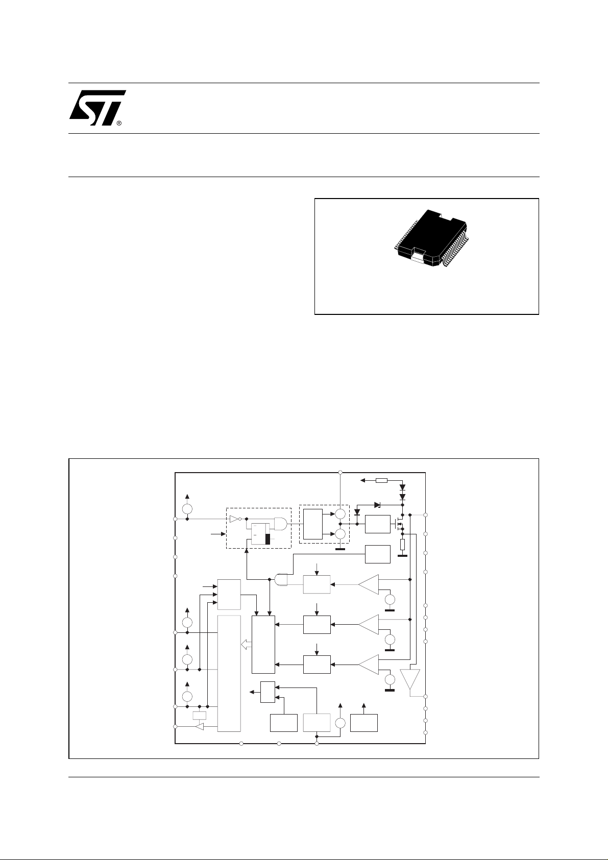
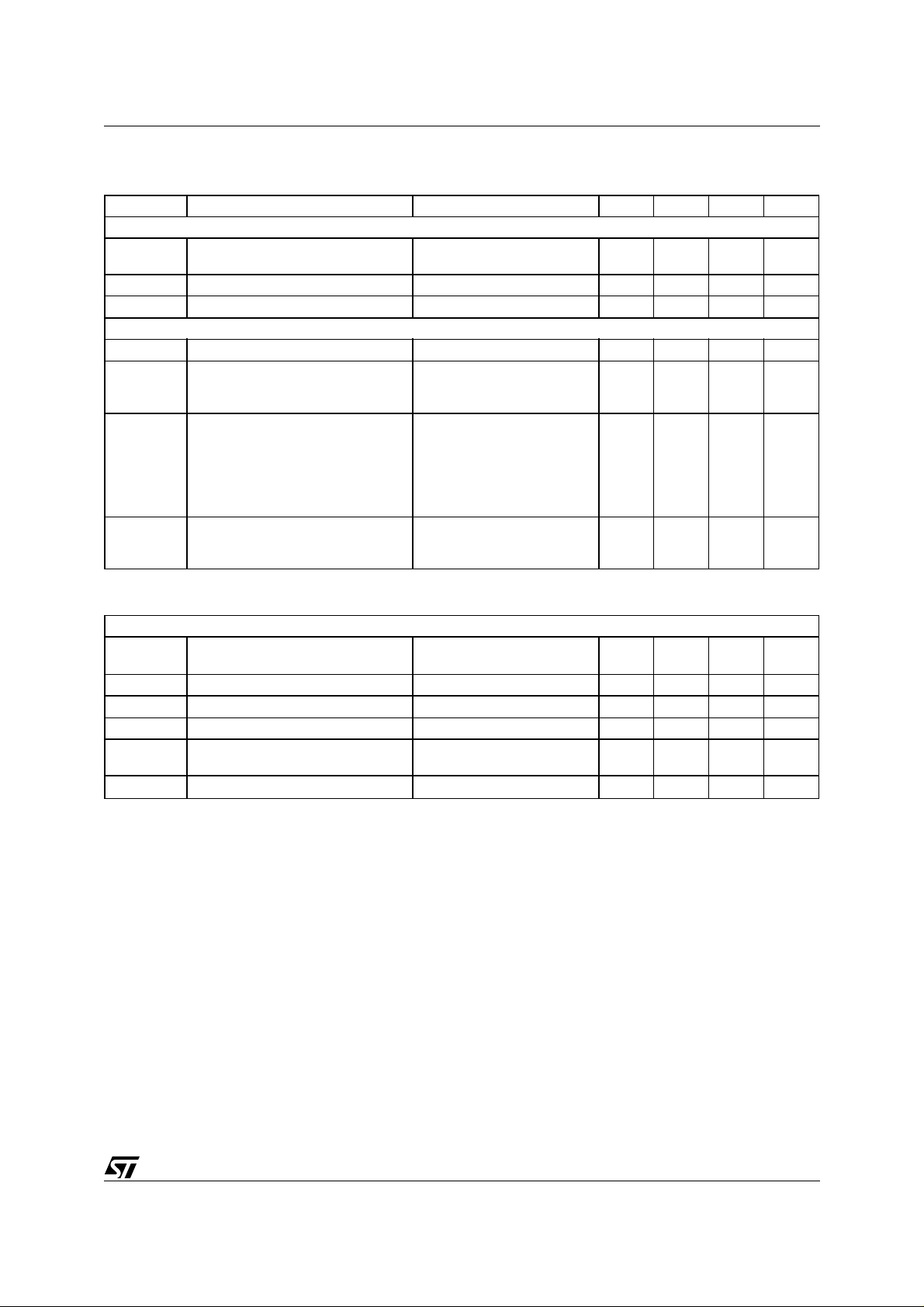
DESCRIPTION
The Quad Driver is an integrated quad low-side
power switch with power limitation, load i nterrupt
and shorted load detection, thermal shutdown, error detection via SPI interface and integrated Z-diodes for output clamping, free running diodes.
BLOCK DIAGRAM
NON1
NON2
NON3
NON4
SDI
CLK
NSC
SDO
99AT0007
V
V
V
V
CC
=
Reset
CC
=
CC
=
CC
=
Reset
IRES
FR
RESET
Shift
Register
Trigger
S
R
IRES
Failure
Register
Reset ≥1
(FR)
Under
voltage
RESET
Driver
NON1
I_SCB Filter
t_SCB
NON1
I_OL Filter
t_OL
NON1
SCG Filter
t_SCG
RESET
NRESSGNDLGND
VCC
=
=
V
CC
=
V
CC
OSC
Oscillator
R
OL
dV/dt
Control
Overtemp.
OUT1
OUT2
OUT3
OUT4
=
=
=
PGND1
PGND2
PGND3
PGND4
CFB1
CFB2
CFB3
CFB4
May 2002
1/17
L9362
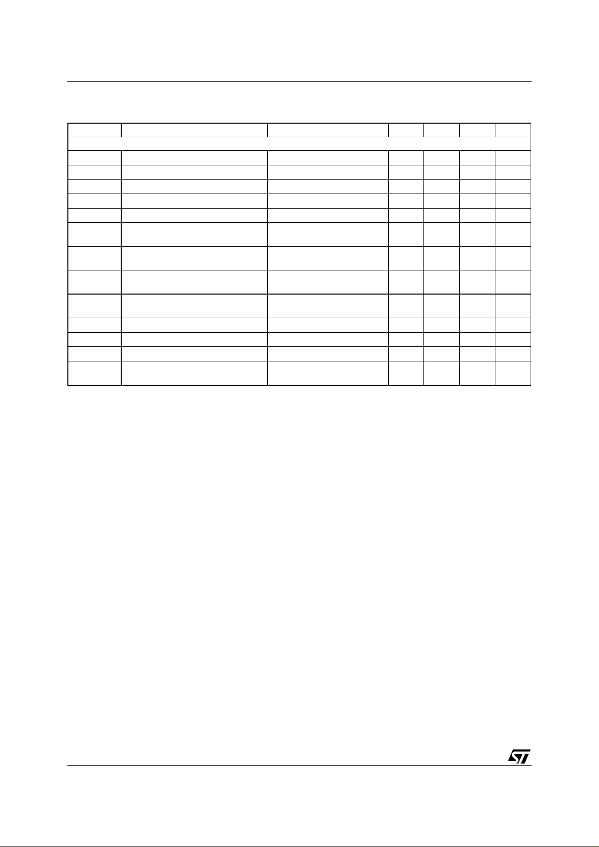
PIN CONNECTION
99AT0012
PGND1
N.C.
CFB1
OUT1
OUT1
CLK
NCS
N.C.
SGND
LGND
N.C.
SDO
SDI
OUT4
OUT4
CFB4
N.C.
PGND4
136
235
334
433
532
631
730
829
928
10 27
11 26
12 25
13 24
14 23
15 22
16 21
17 20
18
Frame connected to PGND
19
PGND2
N.C.
CFB2
OUT2
OUT2
NON1
NON2
N.C.
VCC
N.C.
NRES
NON3
NON4
OUT3
OUT3
CFB3
N.C.
PGND3
PIN FUNCTIONS
Pin No. Pin Name Pin Description Notes
1 PGND1 Power Ground
2 N.C.
3 CFB1 Output Current feedback Sinks current proportional to I
4 OUT1 Output Power Switch
5 OUT1 Output Power Switch
6 CLK Input Clock Digital input, Schmitt trigger, internal Pullup current
7 NCS inverted Chip Select Input Digital input, Schmitt trigger, internal Pullup current
8 N.C.
9 SGND Signal Ground
10 LGND Ground of digital part
11 N.C.
12 SDO Serial Data Output Digital tristate output
13 SDI Serial Data Input Digital input, Schmitt trigger, internal Pullup current
14 OUT4 Output Power Switch
15 OUT4 Output Power Switch
16 CFB4 Output Current feedback Sinks current proportional to I
17 N.C.
18 PGND4 Power Ground
19 PGND3 Power Ground
20 N.C.
21 CFB3 Output Current feedback Sinks current proportional to I
22 OUT3 Output Power Switch
23 OUT3 Output Power Switch
24 NON4 Inverted Control Signal Input Digital input, Schmitt trigger, internal Pullup current
OUT1
OUT4
OUT3
2/17
L9362
PIN FUNCTIONS
(continued)
Pin No. Pin Name Pin Description Notes
25 NON3 Inverted Control Signal Input Digital input, Schmitt trigger, internal Pullup current
26 NRES Inverted Reset Input Digital input, Schmitt trigger, internal Pullup current
27 N.C.
28 VCC 5V Supply Voltage Input
29 N.C.
30 NON2 Inverted Control Signal Input Digital input, Schmitt trigger, internal Pullup current
31 NON1 Inverted Control Signal Input Digital input, Schmitt trigger, internal Pullup current
32 OUT2 Output Power Switch
33 OUT2 Output Power Switch
34 CFB2 Output Current feedback Sinks current proportional to I
OUT2
35 N.C.
36 PGND2 Power Ground
THERMAL DATA
Symbol Parameter Test Conditions Min. Typ. Max. Unit
Thermal resistance
R
th j-case
R
thja
R
thja
ESD
ESD MIL 883C ±2KV
Thermal resistance junction to case
(one powerstage in use)
Die must be
soldered on the
4.5 °C/W
frame.
Thermal resistance junction-ambient pad layout 50 °C/W
Thermal resistance junction-ambient
pad layout + 6 cm
2
35 °C/W
on board heat sink
ABSOLUTE MAXIMUM RATINGS
For externally applied voltages or currents exceeding these limits damage of the circuit may occur
Symbol Parameter Test Conditions Min. Typ. Max. Unit
Supply Voltages
V
CC
Outputs (Out 1 ... 4)
V
Out
I
outc
I
SCBpeak
W
OFF
Inputs (NONx; NCS; CLK; NRES; SDI)
V
IN
Outputs (SDO; CFB)
V
OUT
Operating junction temperature
T
Note: The maxi mum ratings may not be exceeded under an y circumstanc es, not even moment arily and individ ually, as perman ent
Supply voltage -0.3 7 V
Continues output voltage With no reverse
-0.3 45 V
current.
Continues current 3.0 A
Peak output current -10 I_SCB A
Clamped energy at the switching OFF For 2ms, see fig. 8 50 mJ
Input voltage -0.3 7 V
Output voltage -0.3 V
Operating junction temperature -40 150 °C
j
damage to the IC will result.
CC
+0.3
V
3/17
L9362
ELECTRICAL CHARACTERISTICS
≤
VCC ≤ 5.5V, -40°C ≤ TJ ≤ 125°C, unless otherwise specified.
4.5V
Symbol Parameter Test Conditions Min. Typ. Max. Unit
Supply current
I
CCRES
Standby current Without load.
≤ 85°C
T
j
NRES = LOW
I
CCOPM
I
CCLV
Operating mode I
OUT 1 ... 4
= 2A 11 17 mA
Low voltage supply current VCC < 0,5V 80 µA
Inputs (NONx; NCS; CLK; NRES; SDI)
V
INL
V
INH
V
hyst
I
IN
I
IN
Low threshold -0.3 0.2 •
High threshold 0.7 •
Hysteresis 0.85 V
Input leakage current VIN = V
Input current (NONx, NCS, CLK,
V
IN
CC
≤ 0.8•V
CC
SDI)
I
IN NRES
Input current NRES 3 20 µA
Serial Data Output
V
V
I
SDOL
SDOH
SDOL
High output level (I
Low output level (I
= -2mA) V
SDO
= 3.2mA) 0.4 V
SDO
Tristate leakage current (NCS = HIGH;
= 0V ... VCC)
V
SDO
Outputs (Out 1 ... 4)
I
OUTL1
Leakage current 1 (NON = HIGH;
= 14V;
V
OUT
VCC = 5V)
V
W
R
DSON
OVR
OVR
OVR
clpa
OFF
Output clamp voltage V
Clamped energy at the switching
1)
OFF
ON resistance I
Positive output voltage ramp
p1
(with inductive load)
p2
Negative output voltage ramp 80% ... 30% of V
n
(I
clpa
= 0.5A) 45 50 60 V
OUT
For 2ms, see fig. 8 50 mJ
= 2A; Tj = 150°C;
OUT
Tj = 25°C
V
OUT
V
BAT
V
OUT
V
BAT
2)
= 30% ... 80% of
=16V 3)
=
... 0.9 • V
clp
with inductive load
t
dON
t
dOFF
Note 1: Typical lo ads for the zener clamping and the out put voltage ramps are:
Note 2: At 150°C gu aranteed by design and el ectrical characteri sation
Note 3: Tested with resistive load of R
Turn ON delay NON = 50%;
V
OUT
Turn OFF delay NON = 50%;
V
OUT
a) 10Ω, 16mH at all outputs or
b) 25Ω, 160mH
Ω
= 50
load
= 0.8 • V
= 0.3 • V
BAT
BAT
3)
BAT
= 16V
3)
V
CC
20 100 µA
CC
- 0.4
-10 10 µA
250
0.3
0.9 1.35
0.75
0.3 0.9 1.35 V/µs
0410µs
0410µs
1.3 mA
V
CC
V
CC
+0.3
10 µA
10 µA
500
300
2.25
V
V
V
mΩ
mΩ
V/µs
V/µs
4/17
L9362
ELECTRICAL CHARACTERISTICS
≤
4.5V
VCC ≤ 5.5V, -40°C ≤ TJ ≤ 125°C, unless otherwise specified.
(continued)
Symbol Parameter Test Conditions Min. Typ. Max. Unit
Powerstage protection
I
SCB
Short current detection and switch
With filter-time t_SCB. 3.0 5.0 A
off threshold
t_SCB Short circuit switch off delay time 3 30 µs
V
ccmin
VCC undervoltage 3.0 4.0 V
Current feedback
T
Ratio 1ICFB
6)
T
MPS1
/ I
for I
OUT
5)
OUT
=0.4...2A
4)
V
≥ 1.8V 1.45 1.65 2 mA/A
CFB
Temperature stability
±3 ±6%
for 0.4A to < 2.0A, related to
25°C
CURS1
CURlin1
CURlin2
= 0.4A to 2A
for I
OUT
6)
for I
= 0.4A to 1.0A
OUT
for I
= 1.0A to 2.0A
OUT
5)
4)
4)
Current stability
∆gain/Gain at 2A
= -40°C -12 17 %
T
J
= +25°C -6 10 %
T
J
= +125°C -5 5 %
T
J
Linearity Error
(within the calibration points
±0.2 ±1
±0.7
at 0.5A, 1A, 2A)
Note 4: At 150°C gu aranteed by design and el ectrical characteri sation
Note 5: Guaranteed by design and electri cal charact erisatio n
Note 6: Values for T
, CURlin1 and CURlin2 are typical values from testing results
MPS1
Diagnostic
V
REF1
Short to GND threshold voltage for I
≤ 2A 0.390
OUT
•V
CC
0.435
•V
CC
t_SCG Short to GND filter time 140 250 µs
I
OL
Open load threshold current 10 55 mA
t_OL Open load filter time 140 265 µs
R
OL
Pullup resistor at OUT1, OUT2,
2.0 8.0 kΩ
OUT3 and OUT4 for OL detection
T
OFF
Note 7: Guaranteed by meas urement and correlati on
Temperature detection threshold
7)
155 170 190 °C
%
%
V
5/17
L9362
ELECTRICAL CHARACTERISTICS
≤
4.5V
VCC ≤ 5.5V, -40°C ≤ TJ ≤ 125°C, unless otherwise specified.
(continued)
Symbol Parameter Test Conditions Min. Typ. Max. Unit
Serial diagnostic link (external Load capacitor at SDO = 100pF)
f
t
clh
t
t
pcld
t
csdv
t
sclch
clk
cll
Clock frequency 50% duty cycle. 0 3 MHz
Minimum time CLK = HIGH 100 ns
Minimum time CLK = LOW 100 ns
Propagation delay CLK to data at SDO valid. 100 ns
NCS = LOW To data at SDO valid. 100 ns
CLK low before NCS low Setup time CLK to NCS
100 ns
change H/L.
t
hclcl
CLK change L/H after
100 ns
NCS = LOW
t
scld
SDI input setup time CLK change H/L after SDI
20 ns
data valid.
t
hcld
SDI input hold time SDI data hold after CLK
20 ns
change H/L.
t
sclcl
t
hclch
t
pchdz
t
fNCS
CLK low before NCS high 150 ns
CLK high after NCS high 150 ns
NCS L/H to output data float 100 ns
NCS filter-time Pulses ≤ t
fNCS
will be
10 40 ns
ignored.
Note: 8. Input Pin Capacitance of SDI, CLK, NCS, NON1, NON2, NON3, NON4 6pF typical; Output Pin Capacitance of SDO 12pF typica
6/17
 Loading...