

Features
■ Output current up to 1.5 A
■ Output voltages of - 5; - 8; - 12; - 15 V
■ Thermal overload protection
■ Short circuit protection
■ Output transition SOA protection
Description
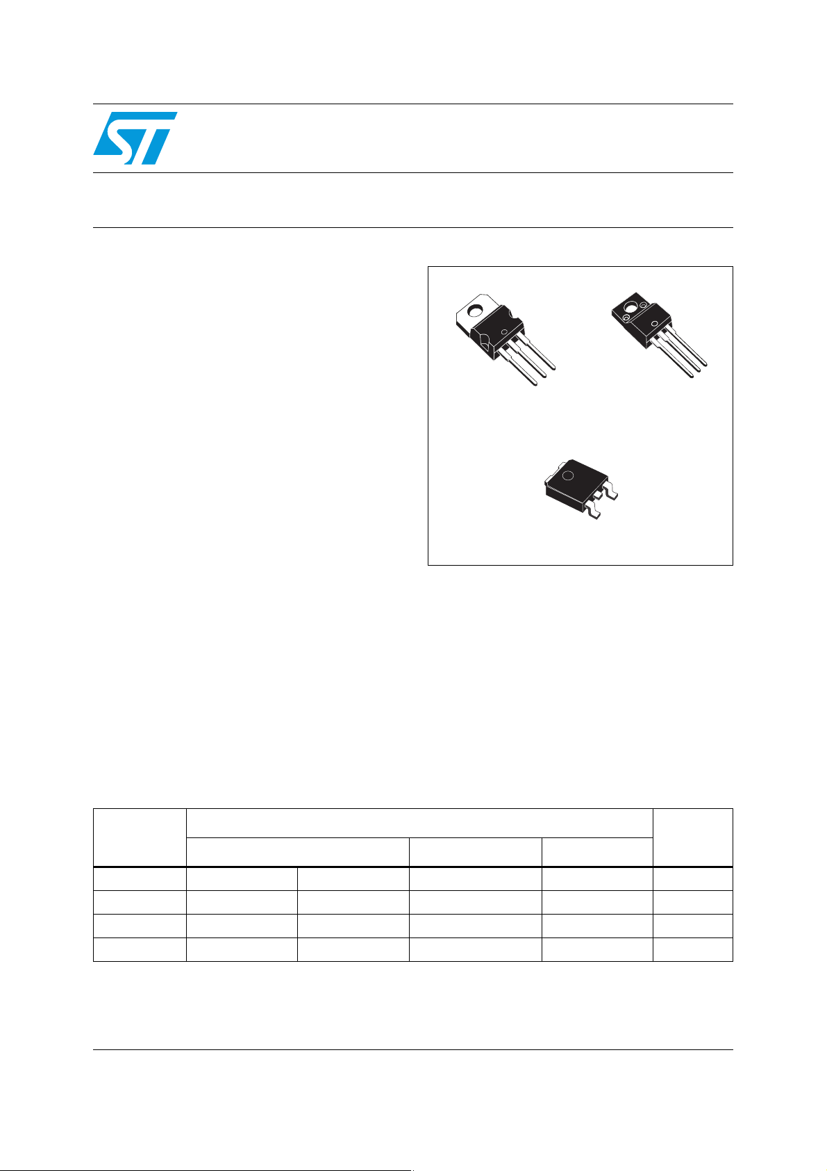
The L79xxC series of three-terminal negative
regulators is available in TO-220, TO-220FP and
D²PAK packages and several fixed output
voltages, making it useful in a wide range of
applications. These regulators can provide local
on-card regulation, eliminating the distribution
problems associated with single point regulation;
furthermore, having the same voltage option as
the L78xx positive standard series, they are
particularly suited for split power supplies. If
adequate heat sinking is provided, they can
deliver over 1.5 A output current. Although
designed primarily as fixed voltage regulators,
these devices can be used with external
components to obtain adjustable voltages and
currents.
L79xxC
Negative voltage regulators
Datasheet − production data
TO-220
D²PAK
TO-220FP
Table 1. Device summary
Order codes
Part numbers
TO-220 D²PAK TO-220FP
L7905C L7905CV L7905CV-DG
L7908C L7908CV L7908CV-DG
L7912C L7912CV L7912CV-DG
L7915C L7915CV L7915CV-DG
1. TO-220 Dual Gauge frame.
May 2012 Doc ID 2149 Rev 21 1/24
This is information on a product in full production.
(1)
(1)
(1)
(1)
L7905CD2T-TR L7905CP - 5 V
L7912CD2T-TR L7912CP - 12 V
L7915CD2T-TR L7915CP - 15 V
Output
voltages
- 8 V
www.st.com
24

Contents L79xxC
Contents
1 Diagram . . . . . . . . . . . . . . . . . . . . . . . . . . . . . . . . . . . . . . . . . . . . . . . . . . . 3
2 Pin configuration . . . . . . . . . . . . . . . . . . . . . . . . . . . . . . . . . . . . . . . . . . . 4
3 Maximum ratings . . . . . . . . . . . . . . . . . . . . . . . . . . . . . . . . . . . . . . . . . . . . 5
4 Test circuit . . . . . . . . . . . . . . . . . . . . . . . . . . . . . . . . . . . . . . . . . . . . . . . . . 6
5 Electrical characteristics . . . . . . . . . . . . . . . . . . . . . . . . . . . . . . . . . . . . . 7
6 Application information . . . . . . . . . . . . . . . . . . . . . . . . . . . . . . . . . . . . . 11
7 Package mechanical data . . . . . . . . . . . . . . . . . . . . . . . . . . . . . . . . . . . . 13
8 Revision history . . . . . . . . . . . . . . . . . . . . . . . . . . . . . . . . . . . . . . . . . . . 23
2/24 Doc ID 2149 Rev 21
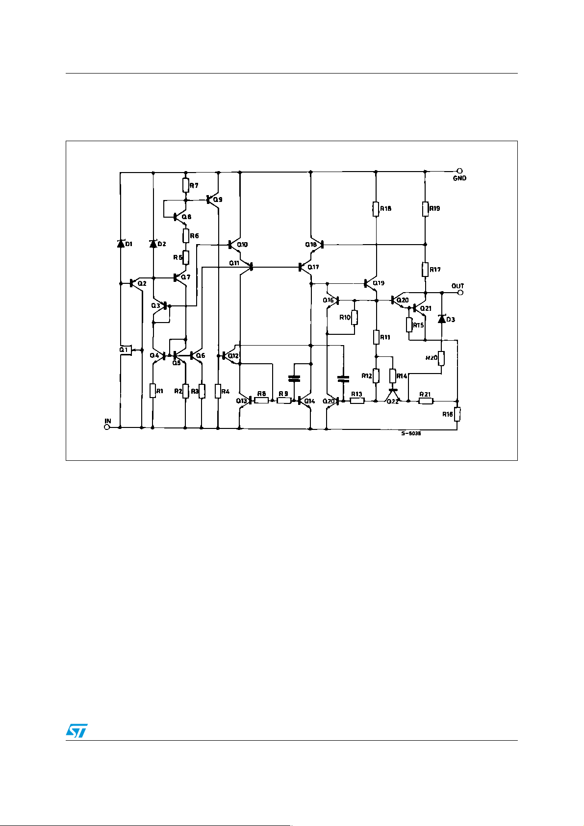
L79xxC Diagram
1 Diagram
Figure 1. Schematic diagram
Doc ID 2149 Rev 21 3/24
Pin configuration L79xxC
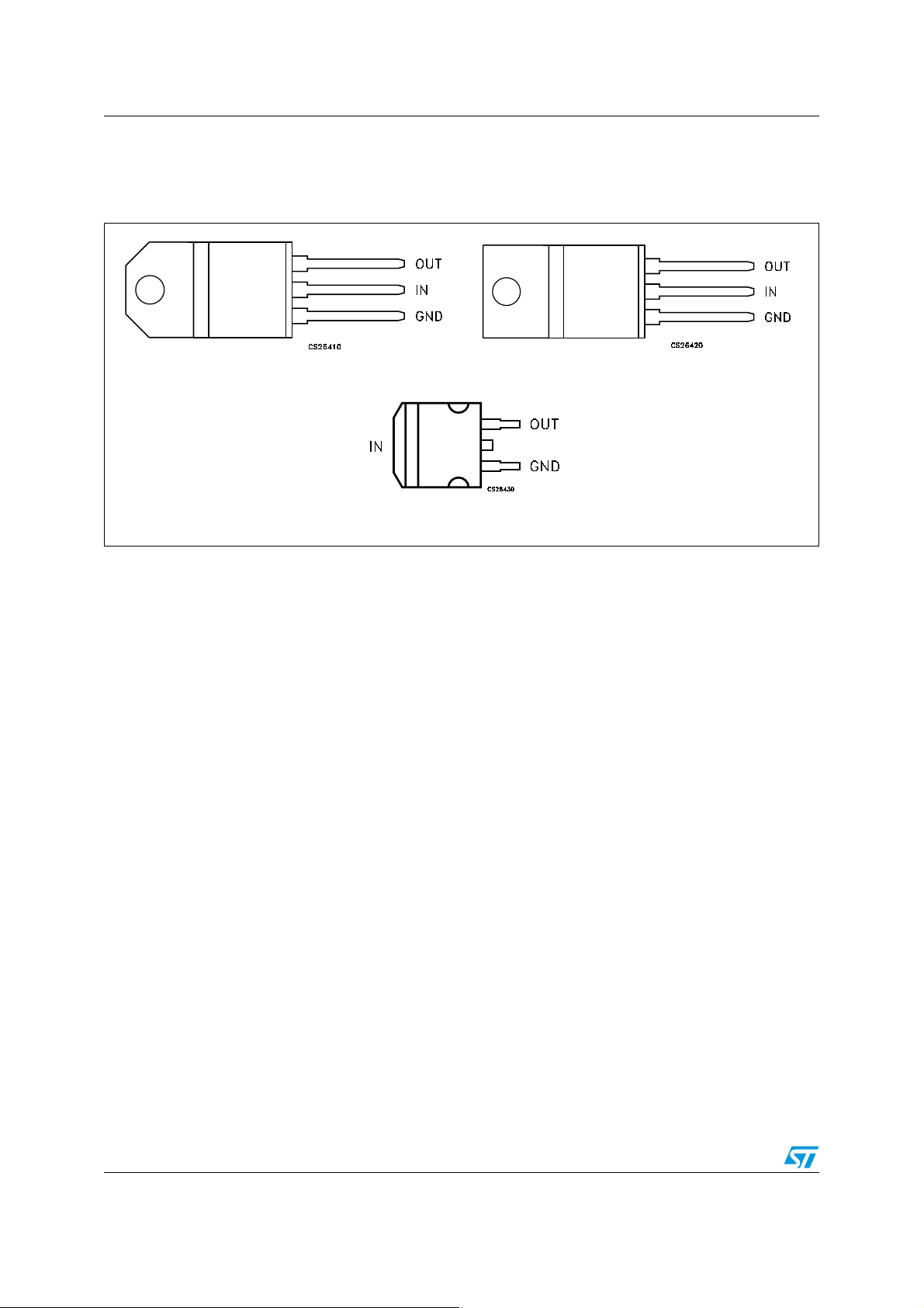
2 Pin configuration
Figure 2. Pin connections (top view)
TO-220
TO220FP
D²PAK (any type)
4/24 Doc ID 2149 Rev 21
L79xxC Maximum ratings
3 Maximum ratings
Table 2. Absolute maximum ratings
Symbol Parameter Value Unit
for V
= - 5 to - 18 V -35
O
= - 20 to - 24 V -40
for V
O
V
T
P
T
V
I
STG
OP
DC input voltage
I
Output current Internally limited
O
Power dissipation Internally limited
D
Storage temperature range -65 to 150 °C
Operating junction temperature range 0 to 150 °C
Note: Absolute maximum ratings are those values beyond which damage to the device may occur.
Functional operation under these condition is not implied.
Table 3. Thermal data
Symbol Parameter D²PAK TO-220 TO-220FP Unit
R
thJC
R
thJA
Thermal resistance junction-case 3 5 5 °C/W
Thermal resistance junction-ambient 62.5 50 60 °C/W
Doc ID 2149 Rev 21 5/24
Test circuit L79xxC
4 Test circuit
Figure 3. Test circuit
6/24 Doc ID 2149 Rev 21
L79xxC Electrical characteristics
5 Electrical characteristics
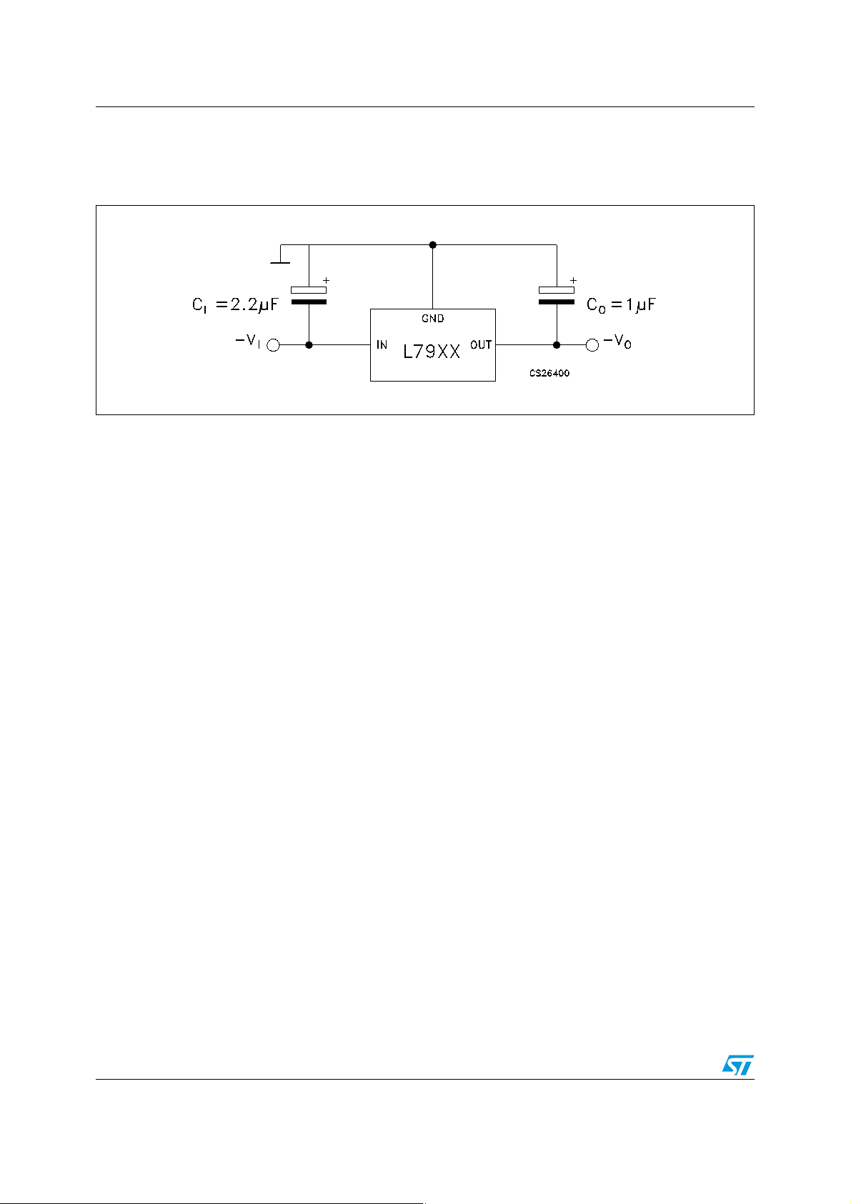
Refer to the test circuits, TJ = 0 to 125 °C, VI = -10 V, IO = 500 mA, CI = 2.2 µF, CO = 1 µF
unless otherwise specified.
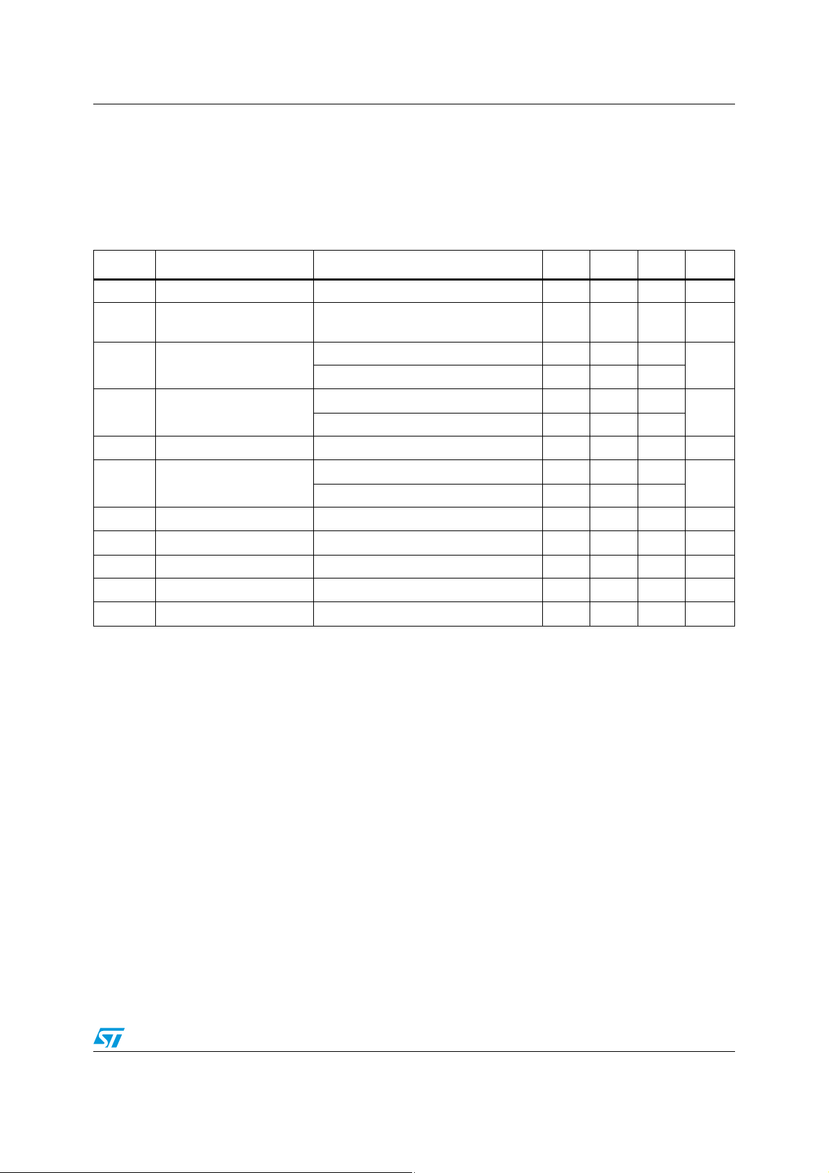
Table 4. Electrical characteristics of L7905C
Symbol Parameter Test conditions Min. Typ. Max. Unit
V
V
ΔV
ΔV
ΔI
ΔV
eN Output noise voltage B = 10Hz to 100kHz, T
Output voltage TJ = 25°C -4.8 -5 -5.2 V
O
= -5 mA to -1 A, PO ≤ 15 W
I
Output voltage
O
(1)
Line regulation
O
(1)
Load regulation
O
I
Quiescent current TJ = 25°C 3 mA
d
Quiescent current change
d
/ΔT Output voltage drift IO = 5 mA -0.4 mV/°C
O
O
= -8 to -20 V
V
I
V
= -7 to -25 V, TJ = 25°C 100
I
= -8 to -12 V, TJ = 25°C 50
V
I
= 5 mA to 1.5 A, TJ = 25°C 100
I
O
-4.75 -5 -5.25 V
IO = 250 to 750 mA, TJ = 25°C 50
I
= 5 mA to 1 A 0.5
O
VI = -8 to -25 V 1.3
= 25°C 100 µV
J
SVR Supply voltage rejection ΔVI = 10 V, f = 120Hz 54 60 dB
V
I
1. Load and line regulation are specified at constant junction temperature. Changes in VO due to heating effects must be
taken into account separately. Pulse testing with low duty cycle is used.
Dropout voltage IO = 1 A, TJ = 25°C, ΔVO = 100 mV 1.4 V
d
Short circuit current 2.1 A
sc
mV
mV
mA
Doc ID 2149 Rev 21 7/24
Electrical characteristics L79xxC
Refer to the test circuits, TJ = 0 to 125 °C, VI = -14 V, IO = 500 mA, CI = 2.2 µF, CO = 1 µF
unless otherwise specified.
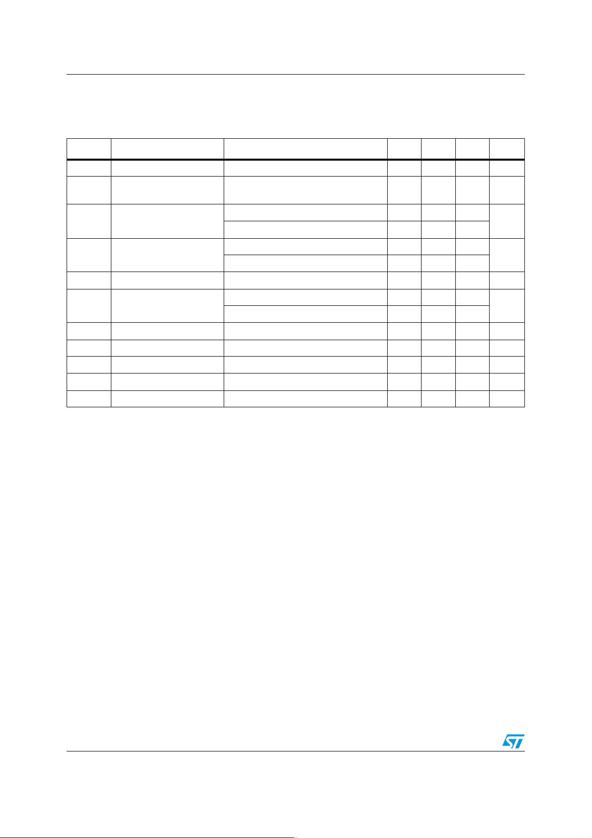
Table 5. Electrical characteristics of L7908C
Symbol Parameter Test conditions Min. Typ. Max. Unit
V
V
ΔV
ΔV
ΔI
ΔV
Output voltage TJ = 25°C -7.7 -8 -8.3 V
O
Output voltage
O
(1)
Line regulation
O
(1)
Load regulation
O
I
Quiescent current TJ = 25°C 3 mA
d
Quiescent current change
d
/ΔT Output voltage drift IO = 5 mA -0.6 mV/°C
O
IO = -5 mA to -1 A, PO ≤ 15 W
V
= -11.5 to -23 V
I
V
= -10.5 to -25 V, TJ = 25°C 160
I
= -11 to -17 V, TJ = 25°C 80
V
I
I
= 5 mA to 1.5 A, TJ = 25°C 160
O
= 250 to 750 mA, TJ = 25°C 80
I
O
I
= 5 mA to 1 A 0.5
O
= -11.5 to -25 V 1
V
I
-7.6 -8 -8.4 V
eN Output noise voltage B = 10Hz to 100kHz, TJ = 25°C 175 µV
SVR Supply voltage rejection ΔV
V
I
1. Load and line regulation are specified at constant junction temperature. Changes in VO due to heating effects must be
taken into account separately. Pulse testing with low duty cycle is used.
Dropout voltage IO = 1 A, TJ = 25°C, ΔVO = 100 mV 1.1 V
d
Short circuit current 1.5 A
sc
= 10 V, f = 120Hz 54 60 dB
I
mV
mV
mA
8/24 Doc ID 2149 Rev 21
 Loading...