

ST L7900 User Manual
查询79XX供应商
■ OUTPUT CURRENT UP TO 1.5A
■ OUTPUT VOLTAGES OF -5; -5.2; -6; -8; -9;
-12; -15; -18; -20 ; -22; -24V
■ THERMAL OVERLOAD PROTECTION
■ SHORT CIRCUIT PROTECTION
■ OUTPUT TRANSITION SOA PROTECTION
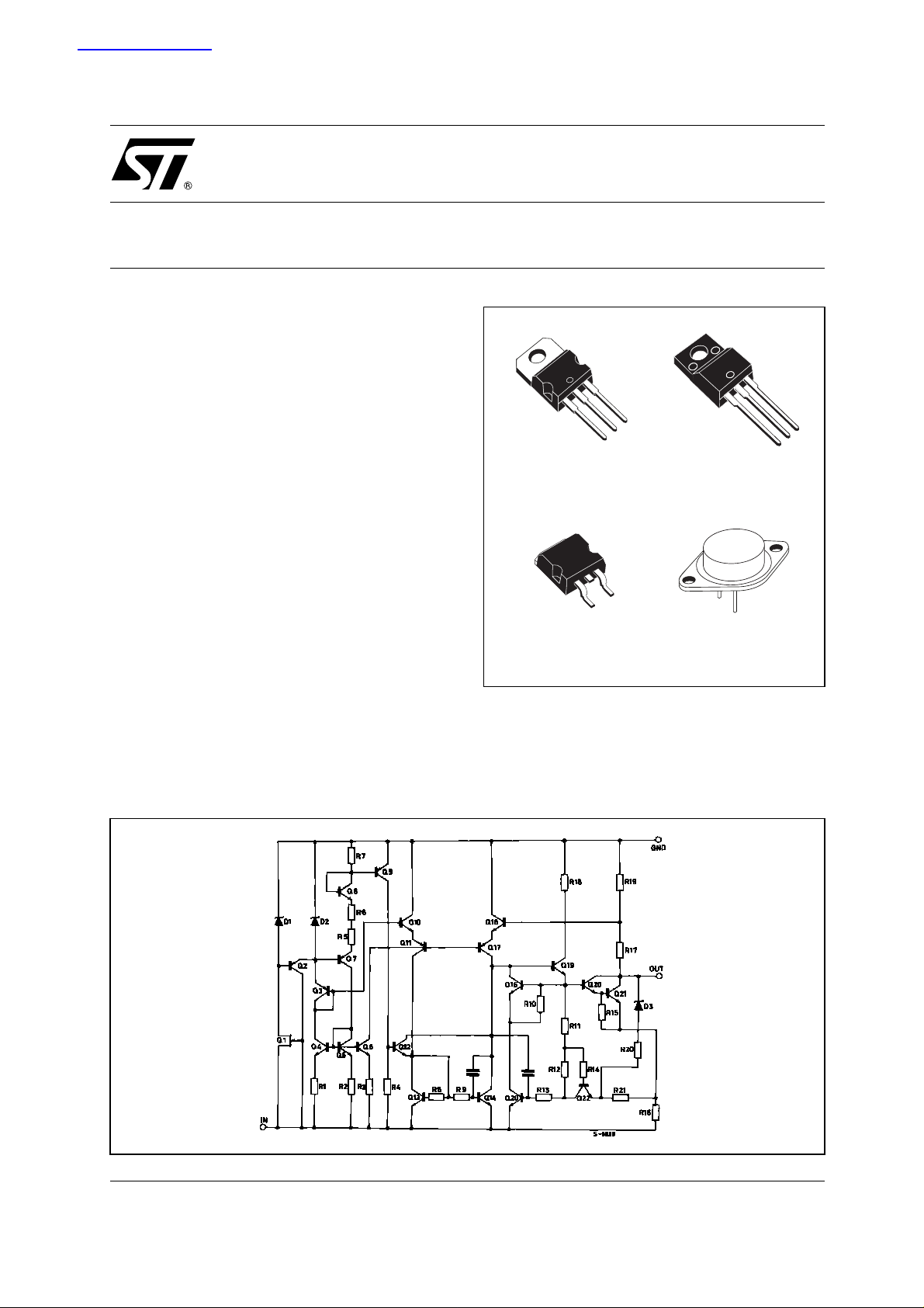
L7900
SERIES
NEGATIVE VOLTAGE REGULATORS
DESCRIPTION
The L7900 series of three-terminal negative
regulators is available in TO-220, TO-220FP,
TO-3 and D
output voltages, making it useful in a wide range of
applications. These regulators c an provide local
on-card regulation, eliminating t he distribution
problems associated with sin gle point regulation;
furthermore, having the same voltage option as
the L7800 positive standard series, they are
particularly suited for split power supplies. In
addition, the -5.2V is also available for ECL
system. If adequate heat sinking is provided, they
can deliver over 1.5A output current.
Although designed primarily as fixed voltage
regulators, thes e devices can be used with
external components to obtain adjust able voltages
and currents.
SCHEMATIC DIAGRAM
2
PAK packages and several fixed
TO-220
D2PAK
TO-220FP
TO-3
1/16February 2003
L7900 SERIE S
ABSOLUTE MAXIMUM RATINGS
Symbol Parameter² Value Unit
V
I
P
T
T
Absolute Maximum Ratings are those values beyond which damage to the device may occur. Functional operation under these condition is
not implied.
DC Input Voltage for VO= 5 to 18V
I
Output Current
O
Power Dissipation
tot
Storage Temperature Range
stg
Operating Junction Temperature Range
op
for V
= 20, 24V
O
THERMAL DATA
-35
-40
Internally Limited
Internally Limited
-65 to 150 °C
0 to 150 °C
V
Symbol Parameter
R
thj-case
R
thj-amb
Thermal Resistance Junction-case Max
Thermal Resistance Junction-ambient Max
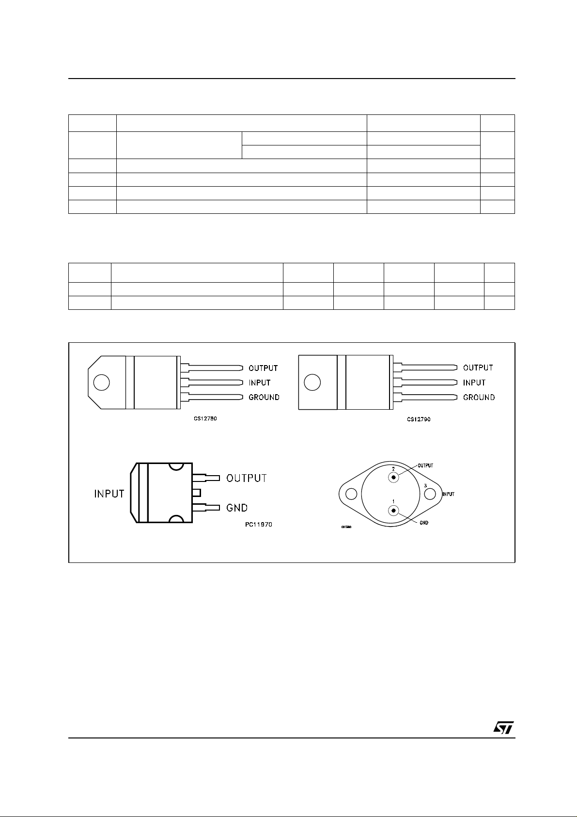
CONNECTION DIAGRAM (top view)
TO-220 TO-220FP
2
PAK
2
PAK
D
TO-220 TO-220FP TO-3 Unit
3354°C/W
62.5 50 60 35 °C/W
TO-3D
2/16
ORDERING CODES
L7900 SERIE S
TYPE TO-220
2
D
PAK (*)
TO-220FP TO-3 OUTPUT VOLTAGE
L7905C L7905CV L7905ACD2T L7905CP L7905CT -5 V
L7952C L7952CV L7952ACD2T L7952CT -5.2 V
L7906C L7906CV L7906ACD2T L7906CP L7906CT -6 V
L7908C L7908CV L7908ACD2T L7908CP L7908CT -8 V
L7912C L7912CV L7912ACD2T L7912CP L7912CT -12 V
L7915C L7915CV L7915ACD2T L7915CP L7915CT -15 V
L7918C L7918CV L7918ACD2T L7918CP L7918CT -18 V
L7920C L7920CV L7920ACD2T L7920CP L7920CT -20 V
L7922C L7922CV L7922ACD2T L7922CT -22 V
L7924C L7924CV L7924ACD2T L7924CP L7924CT -24 V
(*) Available in Tape & Reel with the suffix "-TR".
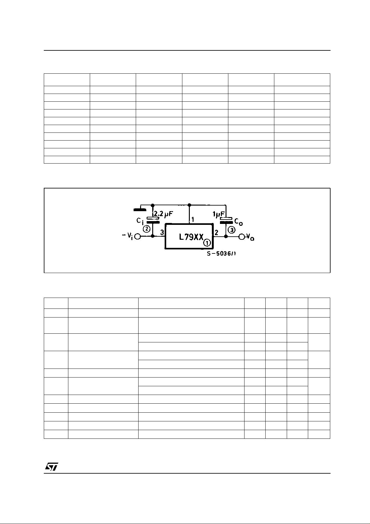
TEST CIRCUIT
ELECTRICAL CHARACTERISTICS O F L7905C (refer to the test circuits, T
I
=500mA,CI=2.2µF,CO= 1 µF unless otherwise specified).
O
= 0 t o 125°C, VI= -10V,
J
Symbol Parameter Test Conditions Min. Typ. Max. Unit
V
Output Voltage TJ= 25°C -4.8 -5 -5.2 V
O
Output Voltage IO=-5mAto-1A PO≤15 W
V
O
(*) Line Regulation VI=-7to-25V TJ= 25°C 100 mV
∆V
O
(*) Load Regulation IO=5mAto1.5A TJ= 25°C 100 mV
∆V
O
Quiescent Current TJ= 25°C 3 mA
I
d
Quiescent Current Change IO=5mAto1A 0.5 mA
∆I
d
/∆T Output Voltage Drift IO= 5 mA -0.4 mV/°C
∆V
O
eN Output Noise Voltage B = 10Hz to 100KHz T
SVR Supply Voltage Rejection ∆V
Dropout Voltage IO=1A TJ= 25°C ∆VO= 100 mV 1.4 V
V
d
Short Circuit Current 2.1 A
I
sc
(*) Load and line regulation are specified at constant junction temperature. Changes in VOdue to heating effects must be taken into account
separately. Pulse testingwith low duty cycle is used.
V
= 8 to 20 V
I
V
=-8to-12V TJ= 25°C 50
I
= 250 to 750 mA TJ= 25°C 50
I
O
= -8 to -25 V 1.3
V
I
= 25°C 100 µV
J
= 10 V f = 120Hz 54 60 dB
I
-4.75 -5 -5.25 V
3/16
L7900 SERIE S
ELECTRICAL CHARACTERISTICS O F L7952C (refer to the test circuits, TJ= 0 t o 125°C, VI= -10V,
I
=500mA,CI=2.2µF,CO= 1 µF unless otherwise specified).
O
Symbol Parameter Test Conditions Min. Typ. Max. Unit
V
Output Voltage TJ= 25°C -5.0 -5.2 -5.4 V
O
Output Voltage IO=-5mAto-1A PO≤15 W
V
O
(*) Line Regulation VI=-8to-25V TJ= 25°C 105 mV
∆V
O
(*) Load Regulation IO=5mAto1.5A TJ= 25°C 105 mV
∆V
O
Quiescent Current TJ= 25°C 3 mA
I
d
Quiescent Current Change IO=5mAto1A 0.5 mA
∆I
d
/∆T Output Voltage Drift IO= 5 mA -0.5 mV/°C
∆V
O
eN Output Noise Voltage B = 10Hz to 100KHz T
SVR Supply Voltage Rejection ∆V
Dropout Voltage IO=1A TJ= 25°C ∆VO= 100 mV 1.4 V
V
d
Short Circuit Current 2 A
I
sc
(*) Load and line regulation are specified at constant junction temperature. Changes in VOdue to heating effects must be taken into account
separately. Pulse testingwith low duty cycle is used.
V
= -9 to -21 V
I
=-9to-12V TJ= 25°C 52
V
I
= 250 to 750 mA TJ= 25°C 52
I
O
= -9 to -25 V 1.3
V
I
= 25°C 125 µV
J
= 10 V f = 120Hz 54 60 dB
I
-4.95 -5.2 -5.45 V
ELECTRICAL CHARACTERISTICS O F L7906C (refer to the test circuits, TJ= 0 t o 125°C, VI= -11V,
=500mA,CI=2.2µF,CO= 1 µF unless otherwise specified).
I
O
Symbol Parameter Test Conditions Min. Typ. Max. Unit
Output Voltage TJ= 25°C -5.75 -6 -6.25 V
V
O
Output Voltage IO=-5mAto-1A PO≤15 W
V
O
(*) Line Regulation VI= -8.5 to -25 V TJ= 25°C 120 mV
∆V
O
(*) Load Regulation IO=5mAto1.5A TJ= 25°C 120 mV
∆V
O
Quiescent Current TJ= 25°C 3 mA
I
d
Quiescent Current Change IO=5mAto1A 0.5 mA
∆I
d
/∆T Output Voltage Drift IO= 5 mA -0.6 mV/°C
∆V
O
eN Output Noise Voltage B = 10Hz to 100KHz T
SVR Supply Voltage Rejection ∆V
Dropout Voltage IO=1A TJ= 25°C ∆VO= 100 mV 1.4 V
V
d
I
Short Circuit Current 2 A
sc
(*) Load and line regulation are specified at constant junction temperature. Changes in VOdue to heating effects must be taken into account
separately. Pulse testingwith low duty cycle is used.
V
= -9.5 to -21.5 V
I
=-9to-15V TJ= 25°C 60
V
I
= 250 to 750 mA TJ= 25°C 60
I
O
= -9.5 to -25 V 1.3
V
I
= 25°C 144 µV
J
= 10 V f = 120Hz 54 60 dB
I
-5.7 -6 -6.3 V
4/16
L7900 SERIE S
ELECTRICAL CHARACTERISTICS O F L7908C (refer to the test circuits, TJ= 0 t o 125°C, VI= -14V,
I
=500mA,CI=2.2µF,CO= 1 µF unless otherwise specified).
O
Symbol Parameter Test Conditions Min. Typ. Max. Unit
V
Output Voltage TJ= 25°C -7.7 -8 -8.3 V
O
Output Voltage IO=-5mAto-1A PO≤15 W
V
O
(*) Line Regulation VI= -10.5 to -25 V TJ= 25°C 160 mV
∆V
O
(*) Load Regulation IO=5mAto1.5A TJ= 25°C 160 mV
∆V
O
Quiescent Current TJ= 25°C 3 mA
I
d
Quiescent Current Change IO=5mAto1A 0.5 mA
∆I
d
/∆T Output Voltage Drift IO= 5 mA -0.6 mV/°C
∆V
O
eN Output Noise Voltage B = 10Hz to 100KHz T
SVR Supply Voltage Rejection ∆V
Dropout Voltage IO=1A TJ= 25°C ∆VO= 100 mV 1.1 V
V
d
Short Circuit Current 1.5 A
I
sc
(*) Load and line regulation are specified at constant junction temperature. Changes in VOdue to heating effects must be taken into account
separately. Pulse testingwith low duty cycle is used.
V
= -11.5 to -23V
I
= -11 to -17 V TJ= 25°C 80
V
I
= 250 to 750 mA TJ= 25°C 80
I
O
= -11.5 to -25V 1
V
I
= 25°C 175 µV
J
= 10 V f = 120Hz 54 60 dB
I
-7.6 -8 -8.4 V
ELECTRICAL CHARACTERISTICS O F L7912C (refer to the test circuits, TJ= 0 t o 125°C, VI= -19V,
=500mA,CI=2.2µF,CO= 1 µF unless otherwise specified).
I
O
Symbol Parameter Test Conditions Min. Typ. Max. Unit
Output Voltage TJ= 25°C -11.5 -12 -12.5 V
V
O
Output Voltage IO=-5mAto-1A PO≤15 W
V
O
(*) Line Regulation VI= -14.5 to -30 V TJ= 25°C 240 mV
∆V
O
(*) Load Regulation IO=5mAto1.5A TJ= 25°C 240 mV
∆V
O
Quiescent Current TJ= 25°C 3 mA
I
d
Quiescent Current Change IO=5mAto1A 0.5 mA
∆I
d
/∆T Output Voltage Drift IO= 5 mA -0.8 mV/°C
∆V
O
eN Output Noise Voltage B = 10Hz to 100KHz T
SVR Supply Voltage Rejection ∆V
Dropout Voltage IO=1A TJ= 25°C ∆VO= 100 mV 1.1 V
V
d
I
Short Circuit Current 1.5 A
sc
(*) Load and line regulation are specified at constant junction temperature. Changes in VOdue to heating effects must be taken into account
separately. Pulse testingwith low duty cycle is used.
V
= -15.5 to -27 V
I
= -16 to -22 V TJ= 25°C 120
V
I
= 250 to 750 mA TJ= 25°C 120
I
O
= -15 to -30 V 1
V
I
= 25°C 200 µV
J
= 10 V f = 120Hz 54 60 dB
I
-11.4 -12 -12.6 V
5/16
 Loading...