

Features
■ Output current to 2 A
■ Output voltages of 5; 7.5; 9; 10; 12; 15; 18; 24 V
■ Thermal overload protection
■ Short circuit protection
■ Output transition SOA protection
L78Sxx
L78SxxC
2 A positive voltage regulators
Datasheet − production data
Description
The L78Sxx series of three-terminal positive
regulators is available in TO-220 and TO-3
packages and several fixed output voltages,
making it useful in a wide range of applications.
These regulators can provide local on-card
regulation, eliminating the distribution problems
associated with single point regulation. Each type
employs internal current limiting, thermal shutdown and safe area protection, making it
essentially indestructible. If adequate heat sinking
is provided, they can deliver over 2 A output
current. Although designed primarily as fixed
voltage regulators, these devices can be used
with external components to obtain adjustable
voltages and currents.
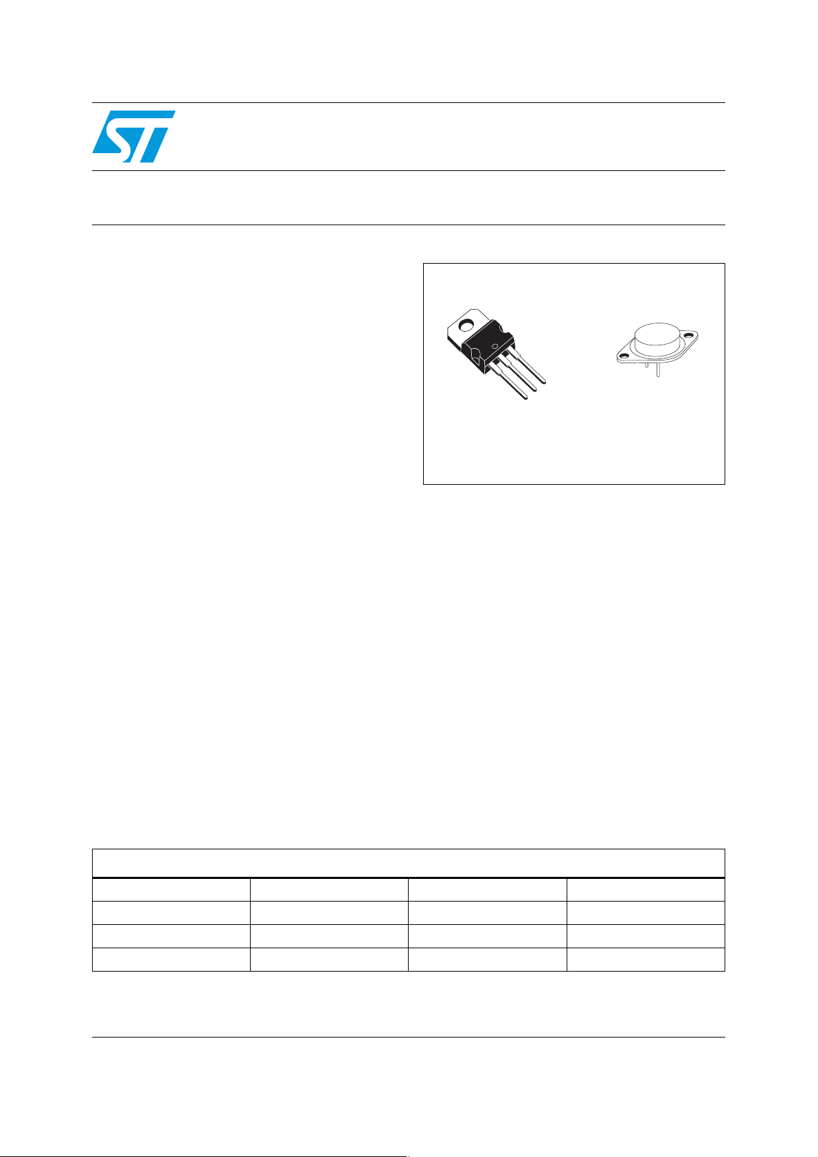
TO-220
TO-3
Table 1. Device summary
Part numbers
L78S05 L78S09 L78S12 L78S18
L78S05C L78S09C L78S12C L78S18C
L78S75 L78S10 L78S15 L78S24
L78S75C L78S10C L78S15C L78S24C
May 2012 Doc ID 2148 Rev 7 1/39
This is information on a product in full production.
www.st.com
39

Contents L78Sxx, L78SxxC
Contents
1 Diagram . . . . . . . . . . . . . . . . . . . . . . . . . . . . . . . . . . . . . . . . . . . . . . . . . . . 5
2 Pin configuration . . . . . . . . . . . . . . . . . . . . . . . . . . . . . . . . . . . . . . . . . . . 6
3 Maximum ratings . . . . . . . . . . . . . . . . . . . . . . . . . . . . . . . . . . . . . . . . . . . . 7
4 Test circuits . . . . . . . . . . . . . . . . . . . . . . . . . . . . . . . . . . . . . . . . . . . . . . . . 8
5 Electrical characteristics . . . . . . . . . . . . . . . . . . . . . . . . . . . . . . . . . . . . . 9
6 Typical performance . . . . . . . . . . . . . . . . . . . . . . . . . . . . . . . . . . . . . . . . 22
7 Package mechanical data . . . . . . . . . . . . . . . . . . . . . . . . . . . . . . . . . . . . 32
8 Order codes . . . . . . . . . . . . . . . . . . . . . . . . . . . . . . . . . . . . . . . . . . . . . . 37
9 Revision history . . . . . . . . . . . . . . . . . . . . . . . . . . . . . . . . . . . . . . . . . . . 38
2/39 Doc ID 2148 Rev 7

L78Sxx, L78SxxC List of tables
List of tables
Table 1. Device summary . . . . . . . . . . . . . . . . . . . . . . . . . . . . . . . . . . . . . . . . . . . . . . . . . . . . . . . . . . 1
Table 2. Absolute maximum ratings . . . . . . . . . . . . . . . . . . . . . . . . . . . . . . . . . . . . . . . . . . . . . . . . . . 7
Table 3. Thermal data. . . . . . . . . . . . . . . . . . . . . . . . . . . . . . . . . . . . . . . . . . . . . . . . . . . . . . . . . . . . . 7
Table 4. Electrical characteristics of L78S05 . . . . . . . . . . . . . . . . . . . . . . . . . . . . . . . . . . . . . . . . . . . 9
Table 5. Electrical characteristics of L78S75 . . . . . . . . . . . . . . . . . . . . . . . . . . . . . . . . . . . . . . . . . . 10
Table 6. Electrical characteristics of L78S09 . . . . . . . . . . . . . . . . . . . . . . . . . . . . . . . . . . . . . . . . . . 10
Table 7. Electrical characteristics of L78S10 . . . . . . . . . . . . . . . . . . . . . . . . . . . . . . . . . . . . . . . . . . 11
Table 8. Electrical characteristics of L78S12 . . . . . . . . . . . . . . . . . . . . . . . . . . . . . . . . . . . . . . . . . . 11
Table 9. Electrical characteristics of L78S15 . . . . . . . . . . . . . . . . . . . . . . . . . . . . . . . . . . . . . . . . . . 12
Table 10. Electrical characteristics of L78S18 . . . . . . . . . . . . . . . . . . . . . . . . . . . . . . . . . . . . . . . . . . 12
Table 11. Electrical characteristics of L78S24 . . . . . . . . . . . . . . . . . . . . . . . . . . . . . . . . . . . . . . . . . . 13
Table 12. Electrical characteristics of L78S05C . . . . . . . . . . . . . . . . . . . . . . . . . . . . . . . . . . . . . . . . . 14
Table 13. Electrical characteristics of L78S75C . . . . . . . . . . . . . . . . . . . . . . . . . . . . . . . . . . . . . . . . . 15
Table 14. Electrical characteristics of L78S09C . . . . . . . . . . . . . . . . . . . . . . . . . . . . . . . . . . . . . . . . . 16
Table 15. Electrical characteristics of L78S10C . . . . . . . . . . . . . . . . . . . . . . . . . . . . . . . . . . . . . . . . . 17
Table 16. Electrical characteristics of L78S12C . . . . . . . . . . . . . . . . . . . . . . . . . . . . . . . . . . . . . . . . . 18
Table 17. Electrical characteristics of L78S15C . . . . . . . . . . . . . . . . . . . . . . . . . . . . . . . . . . . . . . . . . 19
Table 18. Electrical characteristics of L78S18C . . . . . . . . . . . . . . . . . . . . . . . . . . . . . . . . . . . . . . . . . 20
Table 19. Electrical characteristics of L78S24C . . . . . . . . . . . . . . . . . . . . . . . . . . . . . . . . . . . . . . . . . 21
Table 20. TO-220 mechanical data . . . . . . . . . . . . . . . . . . . . . . . . . . . . . . . . . . . . . . . . . . . . . . . . . . 32
Table 21. Order codes . . . . . . . . . . . . . . . . . . . . . . . . . . . . . . . . . . . . . . . . . . . . . . . . . . . . . . . . . . . . 37
Table 22. Document revision history . . . . . . . . . . . . . . . . . . . . . . . . . . . . . . . . . . . . . . . . . . . . . . . . . 38
Doc ID 2148 Rev 7 3/39

List of figures L78Sxx, L78SxxC
List of figures
Figure 1. Block diagram . . . . . . . . . . . . . . . . . . . . . . . . . . . . . . . . . . . . . . . . . . . . . . . . . . . . . . . . . . . . 5
Figure 2. Pin connections (top view) . . . . . . . . . . . . . . . . . . . . . . . . . . . . . . . . . . . . . . . . . . . . . . . . . . 6
Figure 3. Schematic diagram . . . . . . . . . . . . . . . . . . . . . . . . . . . . . . . . . . . . . . . . . . . . . . . . . . . . . . . . 6
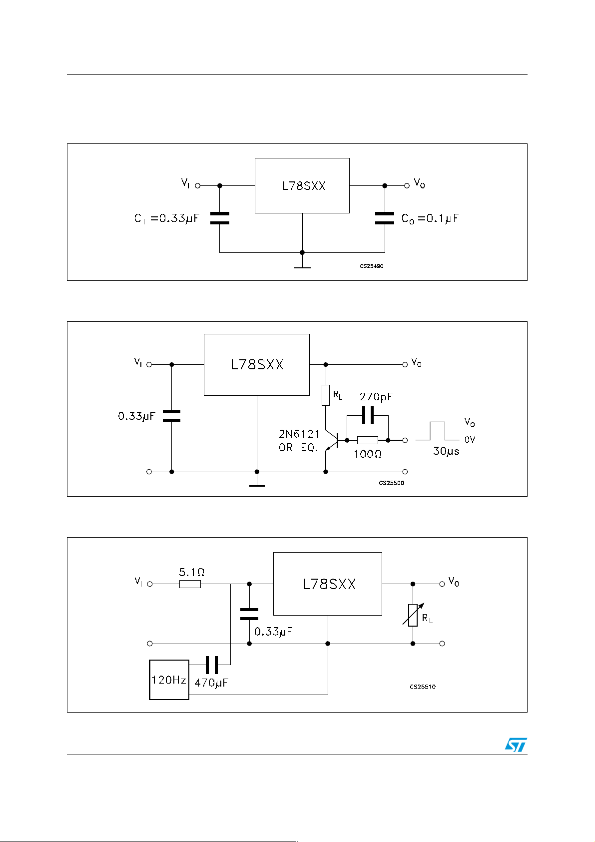
Figure 4. Application circuits . . . . . . . . . . . . . . . . . . . . . . . . . . . . . . . . . . . . . . . . . . . . . . . . . . . . . . . . 7
Figure 5. DC parameter . . . . . . . . . . . . . . . . . . . . . . . . . . . . . . . . . . . . . . . . . . . . . . . . . . . . . . . . . . . . 8
Figure 6. Load regulation . . . . . . . . . . . . . . . . . . . . . . . . . . . . . . . . . . . . . . . . . . . . . . . . . . . . . . . . . . . 8
Figure 7. Ripple rejection . . . . . . . . . . . . . . . . . . . . . . . . . . . . . . . . . . . . . . . . . . . . . . . . . . . . . . . . . . . 8
Figure 8. Dropout voltage vs. junction temperature . . . . . . . . . . . . . . . . . . . . . . . . . . . . . . . . . . . . . . 22
Figure 9. Peak output current vs. input/output differential voltage . . . . . . . . . . . . . . . . . . . . . . . . . . . 22
Figure 10. Output impedance vs. frequency . . . . . . . . . . . . . . . . . . . . . . . . . . . . . . . . . . . . . . . . . . . . 22
Figure 11. Output voltage vs. junction temperature . . . . . . . . . . . . . . . . . . . . . . . . . . . . . . . . . . . . . . . 22
Figure 12. Supply voltage rejection vs. frequency . . . . . . . . . . . . . . . . . . . . . . . . . . . . . . . . . . . . . . . . 22
Figure 13. Quiescent current vs. junction temperature . . . . . . . . . . . . . . . . . . . . . . . . . . . . . . . . . . . . 22
Figure 14. Load transient response . . . . . . . . . . . . . . . . . . . . . . . . . . . . . . . . . . . . . . . . . . . . . . . . . . . 23
Figure 15. Line transient response . . . . . . . . . . . . . . . . . . . . . . . . . . . . . . . . . . . . . . . . . . . . . . . . . . . 23
Figure 16. Quiescent current vs. input voltage . . . . . . . . . . . . . . . . . . . . . . . . . . . . . . . . . . . . . . . . . . 23
Figure 17. Fixed output regulator . . . . . . . . . . . . . . . . . . . . . . . . . . . . . . . . . . . . . . . . . . . . . . . . . . . . . 23
Figure 18. Constant current regulator . . . . . . . . . . . . . . . . . . . . . . . . . . . . . . . . . . . . . . . . . . . . . . . . . 24
Figure 19. Circuit for increasing output voltage . . . . . . . . . . . . . . . . . . . . . . . . . . . . . . . . . . . . . . . . . . 24
Figure 20. Adjustable output regulator (7 to 30 V) . . . . . . . . . . . . . . . . . . . . . . . . . . . . . . . . . . . . . . . . 24
Figure 21. 0.5 to 10 V regulator . . . . . . . . . . . . . . . . . . . . . . . . . . . . . . . . . . . . . . . . . . . . . . . . . . . . . . 25
Figure 22. High current voltage regulator . . . . . . . . . . . . . . . . . . . . . . . . . . . . . . . . . . . . . . . . . . . . . . 25
Figure 23. High output current with short circuit protection . . . . . . . . . . . . . . . . . . . . . . . . . . . . . . . . . 25
Figure 24. Tracking voltage regulator . . . . . . . . . . . . . . . . . . . . . . . . . . . . . . . . . . . . . . . . . . . . . . . . . 26
Figure 25. Positive and negative regulator . . . . . . . . . . . . . . . . . . . . . . . . . . . . . . . . . . . . . . . . . . . . . 26
Figure 26. Negative output voltage circuit . . . . . . . . . . . . . . . . . . . . . . . . . . . . . . . . . . . . . . . . . . . . . . 27
Figure 27. Switching regulator . . . . . . . . . . . . . . . . . . . . . . . . . . . . . . . . . . . . . . . . . . . . . . . . . . . . . . . 27
Figure 28. High input voltage circuit. . . . . . . . . . . . . . . . . . . . . . . . . . . . . . . . . . . . . . . . . . . . . . . . . . . 27
Figure 29. High input voltage circuit. . . . . . . . . . . . . . . . . . . . . . . . . . . . . . . . . . . . . . . . . . . . . . . . . . . 28
Figure 30. High output voltage regulator . . . . . . . . . . . . . . . . . . . . . . . . . . . . . . . . . . . . . . . . . . . . . . . 28
Figure 31. High input and output voltage . . . . . . . . . . . . . . . . . . . . . . . . . . . . . . . . . . . . . . . . . . . . . . . 28
Figure 32. Reducing power dissipation with dropping resistor. . . . . . . . . . . . . . . . . . . . . . . . . . . . . . . 29
Figure 33. Remote shutdown . . . . . . . . . . . . . . . . . . . . . . . . . . . . . . . . . . . . . . . . . . . . . . . . . . . . . . . . 29
Figure 34. Power AM modulator (unity voltage gain, I
Figure 35. Adjustable output voltage with temperature compensation . . . . . . . . . . . . . . . . . . . . . . . . 30
Figure 36. Light controllers (V
Figure 37. Protection against input short-circuit with high capacitance loads . . . . . . . . . . . . . . . . . . . 31
Figure 38. Drawing dimension TO-220 (type STD-ST Dual Gauge) . . . . . . . . . . . . . . . . . . . . . . . . . . 33
Figure 39. Drawing dimension TO-220 (type STD-ST Single Gauge) . . . . . . . . . . . . . . . . . . . . . . . . . 34
Figure 40. Drawing dimension tube for TO-220 Dual Gauge (mm.) . . . . . . . . . . . . . . . . . . . . . . . . . . 35
Figure 41. Drawing dimension tube for TO-220 Single Gauge (mm.) . . . . . . . . . . . . . . . . . . . . . . . . . 35
= VXX + VBE) . . . . . . . . . . . . . . . . . . . . . . . . . . . . . . . . . . . . . . . . . 30
Omin
≤ 1 A) . . . . . . . . . . . . . . . . . . . . . . . . . . . . . . 29
O
4/39 Doc ID 2148 Rev 7
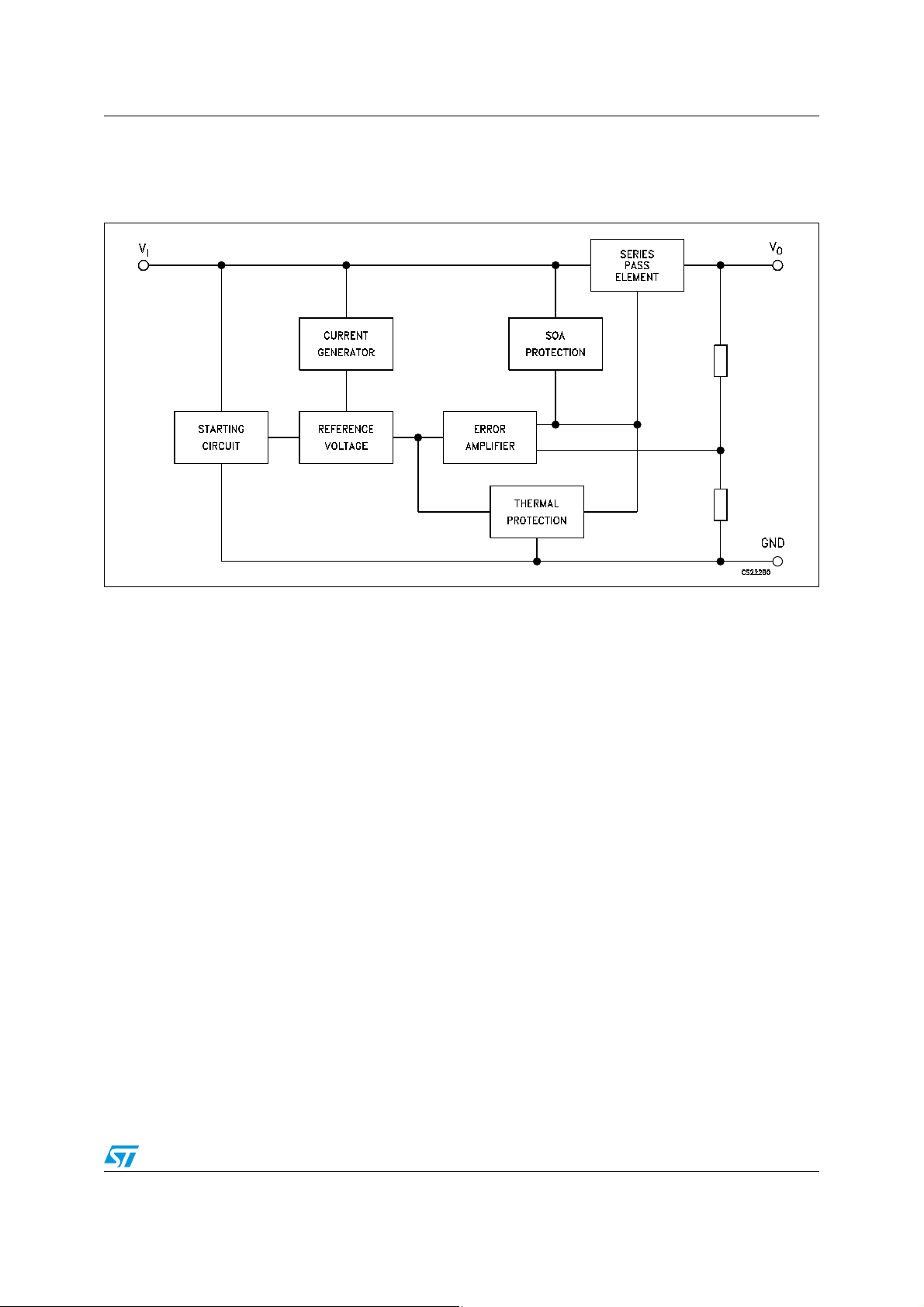
L78Sxx, L78SxxC Diagram
1 Diagram
Figure 1. Block diagram
Doc ID 2148 Rev 7 5/39
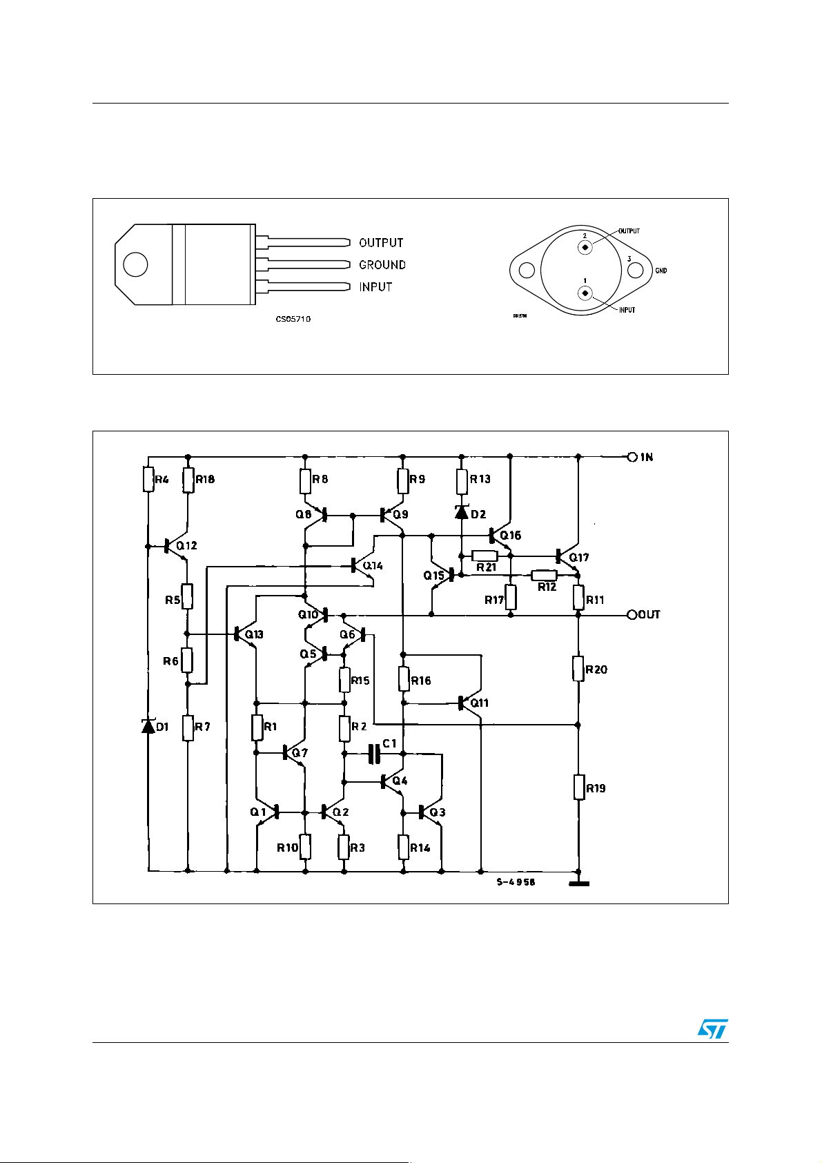
Pin configuration L78Sxx, L78SxxC
2 Pin configuration
Figure 2. Pin connections (top view)
TO-220
Figure 3. Schematic diagram
TO-3
6/39 Doc ID 2148 Rev 7
L78Sxx, L78SxxC Maximum ratings
3 Maximum ratings
Table 2. Absolute maximum ratings
Symbol Parameter Value Unit
for V
= 5 to 18V 35
O
= 24V 40
for V
O
for L78Sxx -55 to 150
for L78SxxC 0 to 150
V
°C
T
P
T
V
I
STG
OP
DC input voltage
I
Output current Internally limited
O
Power dissipation Internally limited
D
Storage temperature range -65 to 150 °C
Operating junction temperature range
Note: Absolute maximum ratings are those values beyond which damage to the device may occur.
Functional operation under these condition is not implied.
Table 3. Thermal data
Symbol Parameter TO-220 TO-3 Unit
R
thJC
R
thJA
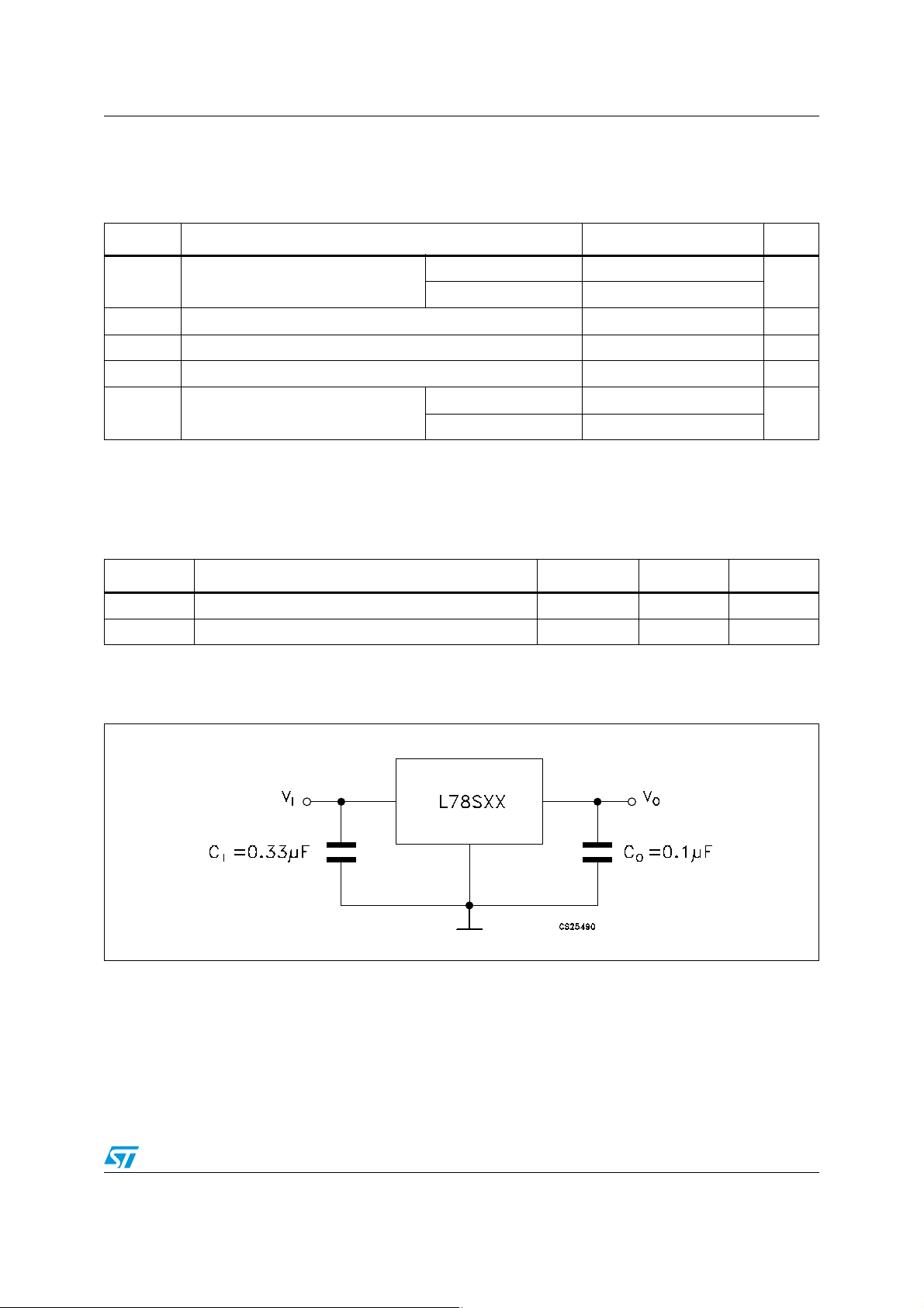
Figure 4. Application circuits
Thermal resistance junction-case 5 4 °C/W
Thermal resistance junction-ambient 50 35 °C/W
Doc ID 2148 Rev 7 7/39
Test circuits L78Sxx, L78SxxC
4 Test circuits
Figure 5. DC parameter
Figure 6. Load regulation
Figure 7. Ripple rejection
8/39 Doc ID 2148 Rev 7
L78Sxx, L78SxxC Electrical characteristics
5 Electrical characteristics
Refer to the test circuits, TJ = 25 °C, VI = 10 V, IO = 500 mA, unless otherwise specified.
Table 4. Electrical characteristics of L78S05
Symbol Parameter Test conditions Min. Typ. Max. Unit
V
V
ΔV
ΔV
ΔI
ΔV
Output voltage 4.8 5 5.2 V
O
Output voltage IO = 1 A, VI = 7 V 4.75 5 5.25 V
O
= 7 to 25 V 100
V
Line regulation
O
Load regulation IO = 20 mA to 2 A 100 mV
O
I
Quiescent current 8 mA
Q
Quiescent current change
Q
/ΔT Output voltage drift IO = 5 mA, TJ = -55 °C to 150 °C -1.1 mV/°C
O
I
VI = 8 to 25 V 50
I
= 20 mA to 1 A 0.5
O
= 7 to 25 V, IO = 20 mA 1.3
V
I
eN Output noise voltage B =10 Hz to 100 kHz 40 µV
SVR Supply voltage rejection f = 120 Hz 60 dB
V
Operating input voltage IO ≤ 1 A 8 V
I
R
I
I
Output resistance f = 1 kHz 17 mΩ
O
Short circuit current VI = 27 V 500 mA
sc
Short circuit peak current 3 A
scp
mV
mA
Doc ID 2148 Rev 7 9/39
Electrical characteristics L78Sxx, L78SxxC
Refer to the test circuits, TJ = 25 °C, VI = 12.5 V, IO = 500 mA, unless otherwise specified.
Table 5. Electrical characteristics of L78S75
Symbol Parameter Test conditions Min. Typ. Max. Unit
V
V
ΔV
ΔV
ΔI
Output voltage 7.15 7.5 7.9 V
O
Output voltage IO = 1 A, VI = 9.5 V 7.1 7.5 7.95 V
O
V
= 9.5 to 25 V 120
Line regulation
O
Load regulation IO = 20 mA to 2 A 120 mV
O
I
Quiescent current 8 mA
Q
Quiescent current change
Q
I
= 10.5 to 20 V 60
V
I
I
= 20 mA to 1 A 0.5
O
= 20 mA, VI = 9.5 to 25 V 1.3
I
O
ΔVO/ΔT Output voltage drift IO = 5 mA, TJ = -55 °C to 150 °C -0.8 mV/°C
eN Output noise voltage B =10 Hz to 100 kHz 52 µV
SVR Supply voltage rejection f = 120 Hz 54 dB
V
Operating input voltage IO ≤ 1.5 A 10.5 V
I
R
I
I
Output resistance f = 1 kHz 16 mΩ
O
Short circuit current VI = 27 V 500 mA
sc
Short circuit peak current 3 A
scp
Refer to the test circuits, TJ = 25 °C, VI = 14 V, IO = 500 mA, unless otherwise specified.
Table 6. Electrical characteristics of L78S09
mV
mA
Symbol Parameter Test conditions Min. Typ. Max. Unit
V
V
ΔV
ΔV
ΔI
ΔV
Output voltage 8.65 9 9.35 V
O
Output voltage IO = 1 A, VI = 11 V 8.6 9 9.4 V
O
V
= 11 to 25 V 130
Line regulation
O
Load regulation IO = 20 mA to 2 A 130 mV
O
I
Quiescent current 8 mA
Q
Quiescent current change
Q
/ΔT Output voltage drift IO = 5 mA, TJ = -55 °C to 150 °C -1 mV/°C
O
I
VI = 11 to 20 V 65
I
= 20mA to 1A 0.5
O
= 11 to 25 V, IO = 20 mA 1.3
V
I
eN Output noise voltage B =10 Hz to 100 kHz 60 µV
SVR Supply voltage rejection f = 120 Hz 53 dB
V
Operating input voltage IO ≤ 1.5 A 12 V
I
R
I
I
Output resistance f = 1 kHz 17 mΩ
O
Short circuit current VI = 27 V 500 mA
sc
Short circuit peak current 3 A
scp
10/39 Doc ID 2148 Rev 7
mV
mA
L78Sxx, L78SxxC Electrical characteristics
Refer to the test circuits, TJ = 25 °C, VI = 15 V, IO = 500 mA, unless otherwise specified.
Table 7. Electrical characteristics of L78S10
Symbol Parameter Test conditions Min. Typ. Max. Unit
V
V
ΔV
ΔV
ΔI
Output voltage 9.5 10 10.5 V
O
Output voltage IO = 1 A, VI = 12.5 V 9.4 10 10.6 V
O
V
= 12.5 to 30 V 200
Line regulation
O
Load regulation IO = 20 mA to 2 A 150 mV
O
I
Quiescent current 8 mA
Q
Quiescent current change
Q
I
= 14 to 22 V 100
V
I
I
= 20 mA to 1A 0.5
O
= 12.5 to 30 V, IO = 20 mA 1
V
I
ΔVO/ΔT Output voltage drift IO = 5 mA, TJ = -55 °C to 150 °C -1 mV/°C
eN Output noise voltage B =10 Hz to 100 kHz 65 µV
SVR Supply voltage rejection f = 120 Hz 53 dB
V
Operating input voltage IO ≤ 1.5 A 13 V
I
R
I
I
Output resistance f = 1 kHz 17 mΩ
O
Short circuit current VI = 27 V 500 mA
sc
Short circuit peak current 3 A
scp
Refer to the test circuits, TJ = 25 °C, VI = 19 V, IO = 500 mA, unless otherwise specified.
Table 8. Electrical characteristics of L78S12
mV
mA
Symbol Parameter Test conditions Min. Typ. Max. Unit
V
V
ΔV
ΔV
ΔI
ΔV
Output voltage 11.5 12 12.5 V
O
Output voltage IO = 1 A, VI = 14.5 V 11.4 12 12.6 V
O
V
= 14.5 to 30 V 240
Line regulation
O
Load regulation IO = 20 mA to 2 A 160 mV
O
I
Quiescent current 8 mA
Q
Quiescent current change
Q
/ΔT Output voltage drift IO = 5 mA, TJ = -55 °C to 150 °C -1 mV/°C
O
I
VI = 16 to 22 V 120
I
= 20 mA to 1 A 0.5
O
= 14.5 to 30 V, IO = 20 mA 1
V
I
mV
mA
eN Output noise voltage B =10 Hz to 100 kHz 75 µV
SVR Supply voltage rejection f = 120 Hz 53 dB
V
Operating input voltage IO ≤ 1.5 A 15 V
I
R
I
I
Output resistance f = 1 kHz 18 mΩ
O
Short circuit current VI = 27 V 500 mA
sc
Short circuit peak current 3 A
scp
Doc ID 2148 Rev 7 11/39

Electrical characteristics L78Sxx, L78SxxC
Refer to the test circuits, TJ = 25 °C, VI = 23 V, IO = 500 mA, unless otherwise specified.
Table 9. Electrical characteristics of L78S15
Symbol Parameter Test conditions Min. Typ. Max. Unit
V
V
ΔV
ΔV
ΔI
Output voltage 14.4 15 15.6 V
O
Output voltage IO = 1 A, VI = 17.5 V 14.25 15 15.75 V
O
V
= 17.5 to 30 V 300
Line regulation
O
Load regulation IO = 20 mA to 2 A 180 mV
O
I
Quiescent current 8 mA
Q
Quiescent current change
Q
I
= 20 to 26 V 150
V
I
I
= 20 mA to 1 A 0.5
O
= 17.5 to 30 V, IO = 20 mA 1
V
I
ΔVO/ΔT Output voltage drift IO = 5 mA, TJ = -55 °C to 150 °C -1 mV/°C
eN Output noise voltage B =10 Hz to 100 kHz 90 µV
SVR Supply voltage rejection f = 120 Hz 52 dB
V
Operating input voltage IO ≤ 1.5 A 18 V
I
R
I
I
Output resistance f = 1 kHz 19 mΩ
O
Short circuit current VI = 27 V 500 mA
sc
Short circuit peak current 3 A
scp
Refer to the test circuits, TJ = 25 °C, VI = 26 V, IO = 500 mA, unless otherwise specified.
Table 10. Electrical characteristics of L78S18
mV
mA
Symbol Parameter Test conditions Min. Typ. Max. Unit
V
V
ΔV
ΔV
ΔI
ΔV
Output voltage 17.1 18 18.9 V
O
Output voltage IO = 1 A, VI = 20.5 V 17 18 19 V
O
V
= 20.5 to 30 V 360
Line regulation
O
Load regulation IO = 20 mA to 2 A 200 mV
O
I
Quiescent current 8 mA
Q
Quiescent current change
Q
/ΔT Output voltage drift IO = 5 mA, TJ = -55 °C to 150 °C -1 mV/°C
O
I
VI = 22 to 28 V 180
I
= 20 mA to 1 A 0.5
O
= 20.5 to 30 V, IO = 20 mA 1
V
I
eN Output noise voltage B =10 Hz to 100 kHz 110 µV
SVR Supply voltage rejection f = 120 Hz 49 dB
V
Operating input voltage IO ≤ 1.5 A 21 V
I
R
I
I
Output resistance f = 1 kHz 22 mΩ
O
Short circuit current VI = 27 V 500 mA
sc
Short circuit peak current 3 A
scp
12/39 Doc ID 2148 Rev 7
mV
mA
 Loading...