

Features
■ Output current to 0.5 A
■ Output voltages of 5; 6; 8; 9; 10; 12; 15; 24 V
■ Thermal overload protection
■ Short circuit protection
■ Output transition SOA protection
■ ± 2 % output voltage tolerance
■ Guaranteed in extended temperature range
Description
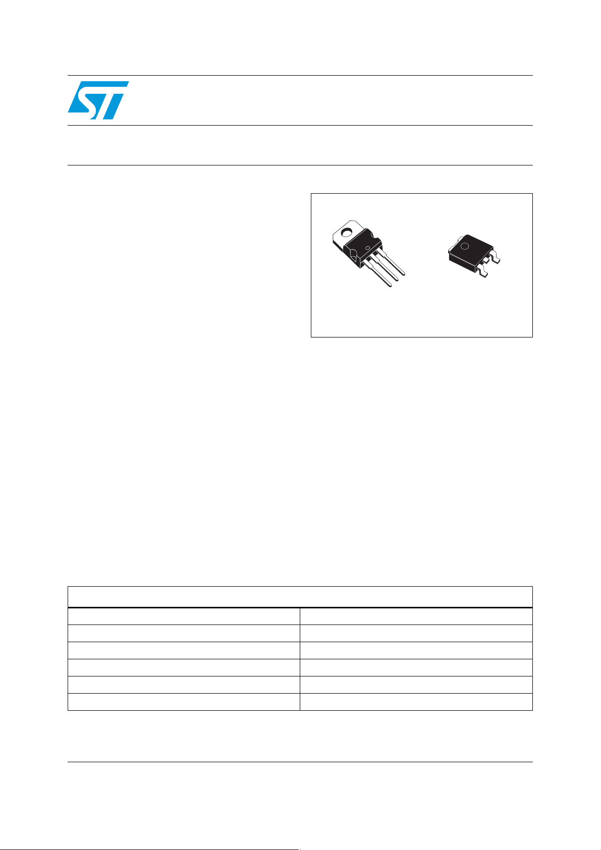
The L78MxxA series of three-terminal positive
regulators is available in TO-220 and DPAK
packages and with several fixed output voltages,
making it useful in a wide range of applications.
These regulators can provide local on-card
regulation eliminating the distribution problems
associated with single point regulation. Each type
employs internal current limiting, thermal
shutdown and safe area protection, making it
essentially indestructible. If adequate heat sinking
is provided, they can deliver over 0.5 A output
current. Although designed primarily as fixed
voltage regulators, these devices can be used
with external components to obtain adjustable
voltage and currents.
L78MxxAB
L78MxxAC
Precision 500 mA regulators
Datasheet − production data
TO-22 0
DPAK
Table 1. Device summary
Part numbers
L78M05AB L78M12AB
L78M05AC L78M12AC
L78M06AB L78M15AB
L78M08AB L78M24AB
L78M09AB L78M24AC
L78M10AB
May 2012 Doc ID 2147 Rev 13 1/31
This is information on a product in full production.
www.st.com
31

Contents L78MxxAB, L78MxxAC
Contents
1 Diagram . . . . . . . . . . . . . . . . . . . . . . . . . . . . . . . . . . . . . . . . . . . . . . . . . . . 3
2 Pin configuration . . . . . . . . . . . . . . . . . . . . . . . . . . . . . . . . . . . . . . . . . . . 4
3 Maximum ratings . . . . . . . . . . . . . . . . . . . . . . . . . . . . . . . . . . . . . . . . . . . . 5
4 Test circuits . . . . . . . . . . . . . . . . . . . . . . . . . . . . . . . . . . . . . . . . . . . . . . . 6
5 Electrical characteristics . . . . . . . . . . . . . . . . . . . . . . . . . . . . . . . . . . . . . 7
6 Typical performance . . . . . . . . . . . . . . . . . . . . . . . . . . . . . . . . . . . . . . . . 15
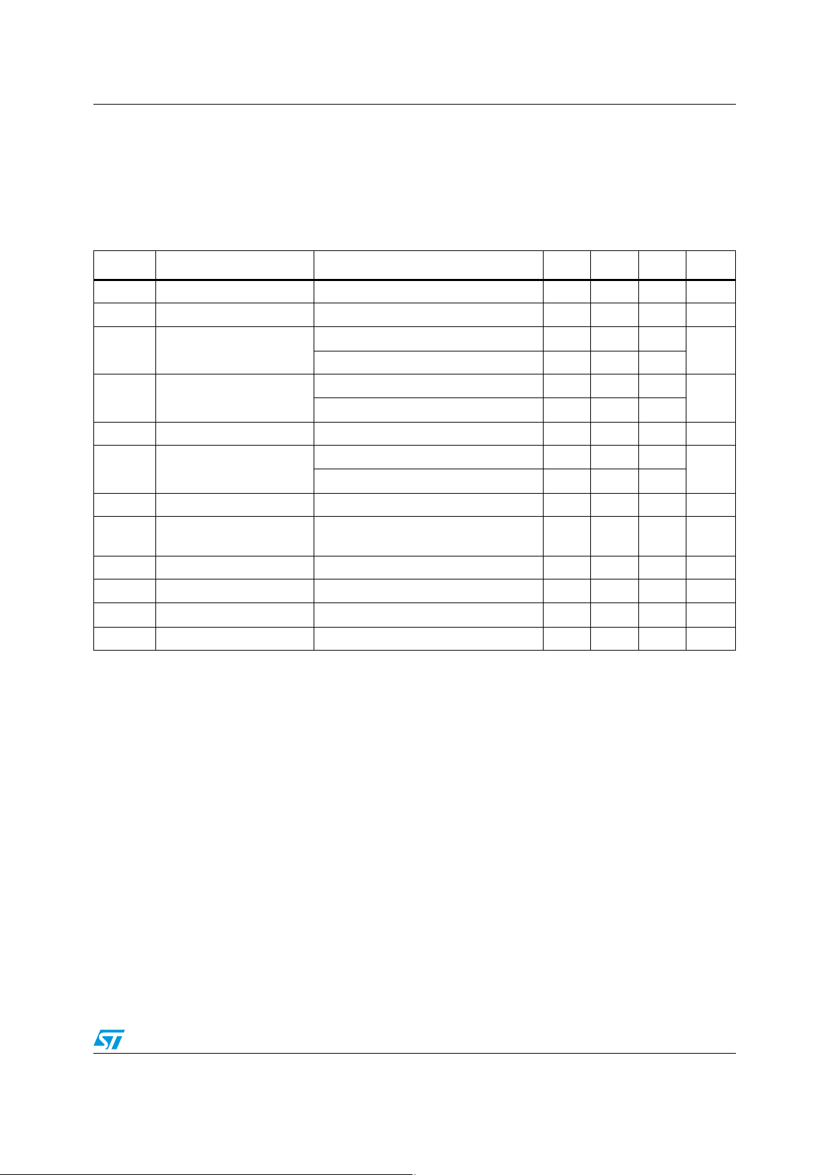
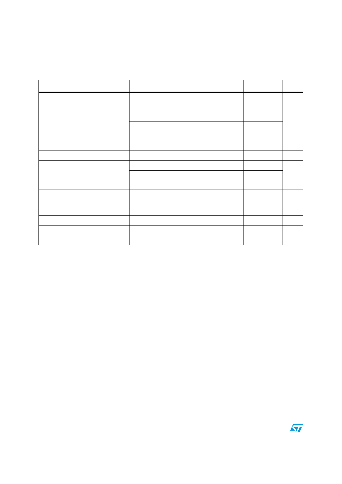
7 Applications information . . . . . . . . . . . . . . . . . . . . . . . . . . . . . . . . . . . . 17
7.1 Design considerations . . . . . . . . . . . . . . . . . . . . . . . . . . . . . . . . . . . . . . . 17
8 Package mechanical data . . . . . . . . . . . . . . . . . . . . . . . . . . . . . . . . . . . . 19
9 Order codes . . . . . . . . . . . . . . . . . . . . . . . . . . . . . . . . . . . . . . . . . . . . . . . 29
10 Revision history . . . . . . . . . . . . . . . . . . . . . . . . . . . . . . . . . . . . . . . . . . . 30
2/31 Doc ID 2147 Rev 13
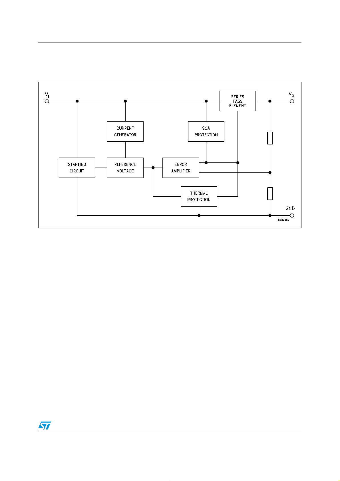
L78MxxAB, L78MxxAC Diagram
1 Diagram
Figure 1. Block diagram
Doc ID 2147 Rev 13 3/31
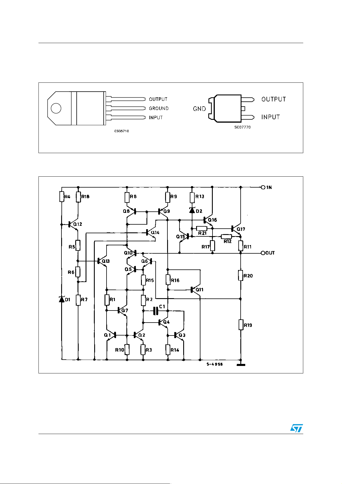
Pin configuration L78MxxAB, L78MxxAC
2 Pin configuration
Figure 2. Pin connections (top view)
DPAKTO-220
Figure 3. Schematic diagram
4/31 Doc ID 2147 Rev 13
L78MxxAB, L78MxxAC Maximum ratings
3 Maximum ratings
Table 2. Absolute maximum ratings
Symbol Parameter Value Unit
for V
= 5 to 18 V 35
O
= 20, 24 V 40
for V
O
for L78M00AC 0 to 125
for L78M00AB -40 to 125
V
°C
T
P
T
V
I
STG
OP
DC input voltage
I
Output current Internally limited mA
O
Power dissipation Internally limited mW
D
Storage temperature range -65 to 150 °C
Operating junction temperature range
Note: Absolute maximum ratings are those values beyond which damage to the device may occur.
Functional operation under these condition is not implied.
Table 3. Thermal data
Symbol Parameter TO-220 DPAK Unit
R
thJC
R
thJA
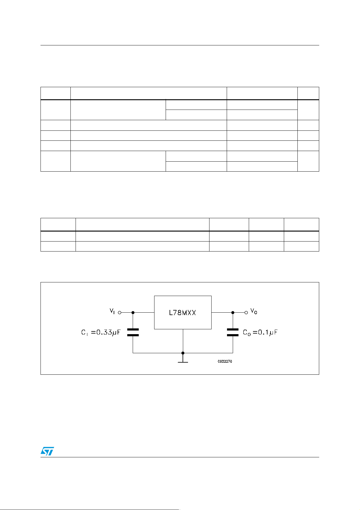
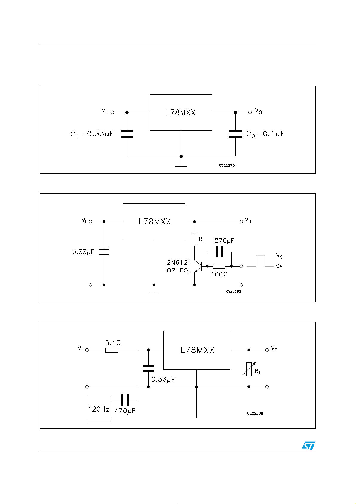
Figure 4. Application circuit
Thermal resistance junction-case 5 8 °C/W
Thermal resistance junction-ambient 50 100 °C/W
Doc ID 2147 Rev 13 5/31
Test circuits L78MxxAB, L78MxxAC
4 Test circuits
Figure 5. DC parameter
Figure 6. Load regulation
Figure 7. Ripple rejection
6/31 Doc ID 2147 Rev 13
L78MxxAB, L78MxxAC Electrical characteristics
5 Electrical characteristics
Refer to the test circuits, VI = 10 V, IO = 350 mA, CI = 0.33 µF, CO = 0.1 µF,
= -40 to 125 °C (AB), TJ = 0 to 125 °C (AC) unless otherwise specified.
T
J
Table 4. Electrical characteristics of L78M05XX
Symbol Parameter Test conditions Min. Typ. Max. Unit
V
V
ΔV
ΔV
ΔI
Output voltage TJ = 25°C 4.9 5 5.1 V
O
Output voltage IO = 5 to 350 mA, VI = 7 to 20 V 4.8 5 5.2 V
O
= 7 to 25 V, IO = 200 mA, TJ = 25°C 100
V
Line regulation
O
Load regulation
O
I
Quiescent current TJ = 25°C 6 mA
d
Quiescent current change
d
I
VI = 8 to 25 V, IO = 200 mA, TJ = 25°C 50
I
= 5 to 500 mA, TJ = 25°C 100
O
= 5 to 200 mA, TJ = 25°C 50
I
O
I
= 5 to 350 mA 0.5
O
= 200 mA, VI = 8 to 25 V 0.8
I
O
mV
mV
mA
ΔVO/ΔT Output voltage drift IO = 5 mA -0.5 mV/°C
= 8 to 18 V, f = 120Hz, IO = 300mA,
V
SVR Supply voltage rejection
I
= 25°C
T
J
62 dB
eN Output noise voltage B =10Hz to 100kHz, TJ = 25°C 40 µV
V
I
I
Dropout voltage TJ = 25°C 2 V
d
Short circuit current TJ = 25°C, VI = 35 V 300 mA
sc
Short circuit peak current TJ = 25°C 700 mA
scp
Doc ID 2147 Rev 13 7/31
Electrical characteristics L78MxxAB, L78MxxAC
Refer to the test circuits, VI = 11 V, IO = 350 mA, CI = 0.33 µF, CO = 0.1 µF,
T
= -40 to 125 °C (AB), TJ = 0 to 125 °C (AC) unless otherwise specified.
J
Table 5. Electrical characteristics of L78M06XX
Symbol Parameter Test conditions Min. Typ. Max. Unit
V
V
ΔV
ΔV
ΔI
ΔV
SVR Supply voltage rejection
Output voltage TJ = 25°C 5.88 6 6.12 V
O
Output voltage IO = 5 to 350 mA, VI = 8 to 21 V 5.75 6 6.3 V
O
V
= 8 to 25 V, IO = 200 mA, TJ = 25°C 100
Line regulation
O
Load regulation
O
I
Quiescent current TJ = 25°C 6 mA
d
Quiescent current change
d
/ΔT Output voltage drift IO = 5 mA -0.5 mV/°C
O
I
= 9 to 25 V, IO = 200 mA, TJ = 25°C 30
V
I
= 5 to 500 mA, TJ = 25°C 120
I
O
IO = 5 to 200 mA, TJ = 25°C 60
= 5 to 350 mA 0.5
I
O
IO = 200 mA, VI = 9 to 25 V 0.8
= 9 to 19 V, f = 120Hz, IO = 300mA,
V
I
T
= 25°C
J
59 dB
eN Output noise voltage B =10Hz to 100kHz 45 µV
V
I
I
Dropout voltage TJ = 25°C 2 V
d
Short circuit current TJ = 25°C, VI = 35 V 270 mA
sc
Short circuit peak current TJ = 25°C 700 mA
scp
mV
mV
mA
8/31 Doc ID 2147 Rev 13
L78MxxAB, L78MxxAC Electrical characteristics
Refer to the test circuits, VI = 14 V, IO = 350 mA, CI = 0.33 µF, CO = 0.1 µF, TJ = -40 to 125
°C (AB), T
Table 6. Electrical characteristics of L78M08XX
Symbol Parameter Test conditions Min. Typ. Max. Unit
= 0 to 125 °C (AC) unless otherwise specified).
J
V
V
ΔV
ΔV
ΔI
ΔV
SVR Supply voltage rejection
eN Output noise voltage B =10Hz to 100kHz, T
V
I
I
Output voltage TJ = 25°C 7.84 8 8.16 V
O
Output voltage IO = 5 to 350 mA, VI = 10.5 to 23 V 7.7 8 8.3 V
O
VI = 10.5 to 25 V, IO = 200 mA,
= 25°C
T
Line regulation
O
Load regulation
O
I
Quiescent current TJ = 25°C 6 mA
d
Quiescent current change
d
/ΔT Output voltage drift IO = 5 mA -0.5 mV/°C
O
Dropout voltage TJ = 25°C 2 V
d
Short circuit current TJ = 25°C, VI = 35 V 250 mA
sc
Short circuit peak current TJ = 25°C 700 mA
scp
J
= 11 to 25 V, IO = 200 mA, TJ = 25°C 30
V
I
I
= 5 to 500 mA, TJ = 25°C 160
O
= 5 to 200 mA, TJ = 25°C 80
I
O
I
= 5 to 350 mA 0.5
O
= 200 mA, VI = 10.5 to 25 V 0.8
I
O
VI = 11.5 to 21.5 V, f = 120Hz
= 300mA, TJ = 25°C
I
O
= 25°C 52 µV
J
56 dB
100
mV
mV
mA
Doc ID 2147 Rev 13 9/31
Electrical characteristics L78MxxAB, L78MxxAC
Refer to the test circuits, VI = 15 V, IO = 350 mA, CI = 0.33 µF, CO = 0.1 µF,
T
= -40 to 125 °C (AB), TJ = 0 to 125 °C (AC) unless otherwise specified).
J
Table 7. Electrical characteristics of L78M09XX
Symbol Parameter Test conditions Min. Typ. Max. Unit
V
V
ΔV
ΔV
ΔI
ΔV
SVR Supply voltage rejection
eN Output noise voltage B =10Hz to 100kHz, T
V
I
I
Output voltage TJ = 25°C 8.82 9 9.18 V
O
Output voltage IO = 5 to 350 mA, VI = 11.5 to 24 V 8.64 9 9.36 V
O
VI = 11.5 to 25 V, IO = 200 mA,
= 25°C
T
Line regulation
O
Load regulation
O
I
Quiescent current TJ = 25°C 6 mA
d
Quiescent current change
d
/ΔT Output voltage drift IO = 5 mA -0.5 mV/°C
O
Dropout voltage TJ = 25°C 2 V
d
Short circuit current VI = 35 V, TJ = 25°C 250 mA
sc
Short circuit peak current TJ = 25°C 700 mA
scp
J
= 12 to 25 V, IO = 200 mA, TJ = 25°C 30
V
I
I
= 5 to 500 mA, TJ = 25°C 180
O
= 5 to 200 mA, TJ = 25°C 90
I
O
I
= 5 to 350 mA 0.5
O
= 200 mA, VI = 11.5 to 25 V 0.8
I
O
VI = 12.5 to 23 V, f = 120Hz,
= 300mA, TJ = 25°C
I
O
= 25°C 52 µV
J
56 dB
100
mV
mV
mA
10/31 Doc ID 2147 Rev 13
 Loading...