


PRECISION 500mA REGULATORS
■ OUTPUT CURRENT TO 0.5A
■ OUTPUT VOLTAGES OF 5; 6; 8; 9; 10; 12;
15; 18; 20; 24V
■ THERMAL OVERLOAD PROTECTION
■ SHORT CIRCUIT PROTECTION
■ OUTPUT TRANSITION SOA PROTECTION
■ ±2% OUTPUT VOLTAGE TOLERANCE
■ GUARANTEED INEXTENDED
TEMPERATURE RANGE
DESCRIPTION
The L78M00AB series of three-terminal positive
regulators is available in TO-220 and DPAK
packages and with several fixed outp ut voltages,
making it useful in a wide range of applications.
These regulators can provide local on-card
regulation eliminating the distribution problems
associated with single point regulation. Each type
employs internal current limiting, thermal
shut-down and safe area protection, making it
essentially indestructible. If adequate heat sinking
is provided, they can deliver over 0.5A output
current. Although designed primarily as fixed
L78M00AB/AC
SERIES
TO-220
DPAK
voltage regulators, these devices can be used
with external components to obtain adjustable
voltage an d currents.
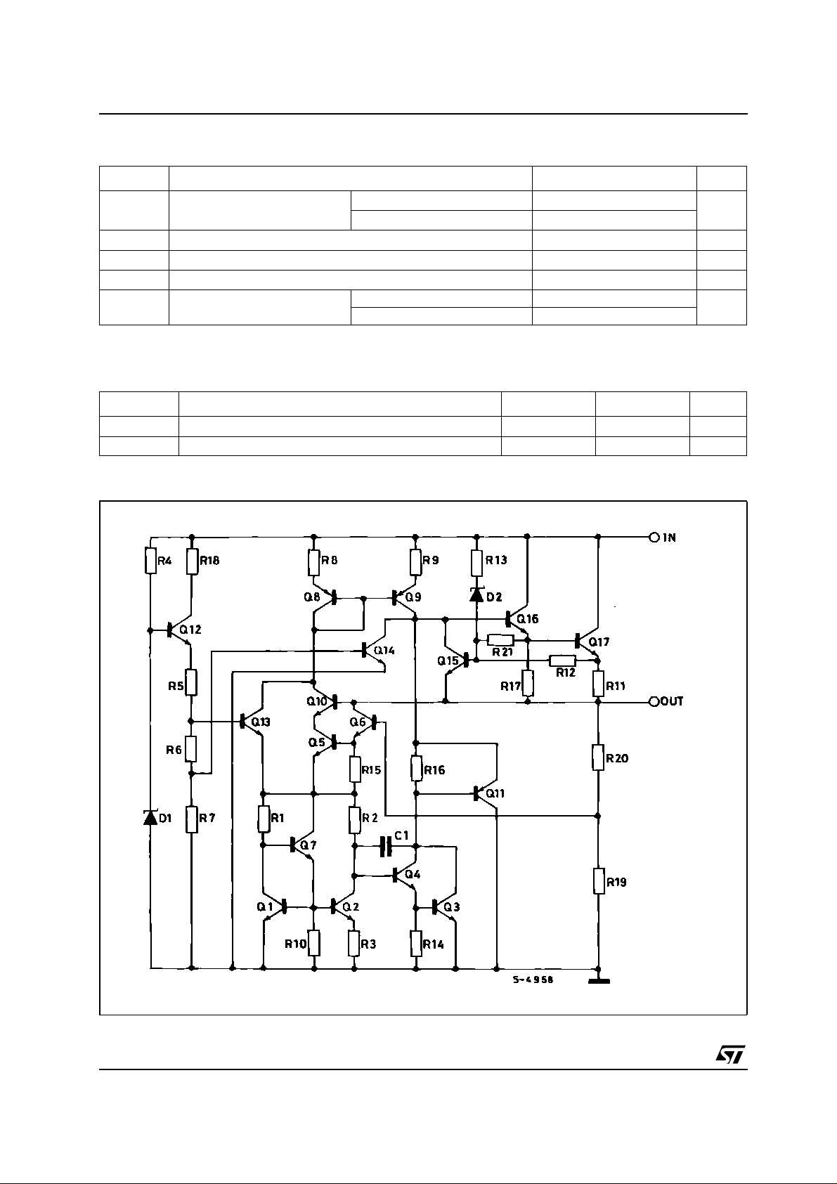
SCHEMATIC DIAGRAM
1/17October 2003
L78M00AB/AC SERIES
ABSOLUTE MAXIMUM RATINGS
Symbol Parameter² Value Unit
V
I
P
T
T
Absolute Maximum Ratings are those values beyond which damage to the device may occur. Functional operation under these condition is
not implied.
DC Input Voltage for VO= 5 to 18V
I
Output Current
O
Power Dissipation
tot
Storage Temperature Range
stg
OperatingJunctionTemperature
op
Range
= 20, 24V
for V
O
for L78M00AC 0 to 125
for L78M00AB -40 to 125
THERMAL DATA
Symbol Parameter TO-220 DPAK Unit
R
thj-case
R
thj-amb
Thermal Resistance Junction-case MAX
Thermal Resistance Junction-ambient MAX
38°C/W
50 100 °C/W
SHEMATIC DIAGRAM
35
40
Internally Limited
Internally Limited
-65 to +150 °C
V
°C
2/17

CONNECTION DIAGRAM (t op v iew)
TO-220 DPAK
ORDERING CODES
TYPE TO-220 DPAK (*) OUTPUT VOLTAGE
L78M05AB L78M05ABV L78M05ABDT 5 V
L78M05AC L78M05ACDT 5 V
L78M06AB L78M06ABV L78M06ABDT 6 V
L78M06AC L78M06ACDT 6 V
L78M08AB L78M08ABV L78M08ABDT 8 V
L78M08AC L78M08ACDT 8 V
L78M09AB L78M09ABV L78M09ABDT 9 V
L78M09AC L78M09ACDT 9 V
L78M10AB L78M10ABV L78M10ABDT 10 V
L78M10AC L78M10ACDT 10 V
L78M12AB L78M12ABV L78M12ABDT 12 V
L78M12AC L78M12ACDT 12 V
L78M15AB L78M15ABV L78M15ABDT 15 V
L78M15AC L78M15ACDT 15 V
L78M18AB L78M18ABV L78M18ABDT 18 V
L78M18AC L78M18ACDT 18 V
L78M20AB L78M20ABV L78M20ABDT 20 V
L78M20AC L78M20ACDT 20 V
L78M24AB L78M24ABV L78M24ABDT 24 V
L78M24AC L78M24ACDT 24 V
L78M00AB/AC SE RIES
(*) Available in Tape & Reel with the suffix "-TR".
APPLICATION CIRCUITS
3/17

L78M00AB/AC SERIES
TEST CIRCUITS
Figure1 : DC Parameter
Figure2 : Load Regulation
Figure3 : Ripple Rejection
4/17
L78M00AB/AC SE RIES
ELECTRICAL CHARACTERISTICS OF L78M05XX (refer to the t est circuits, VI= 10V, IO=350mA,
C
=0.33µF,CO=0.1µF,TJ= -40 to 125°C (AB), TJ= 0 to 125°C (AC) unless otherwise specified)
I
Symbol Parameter Test Conditions Min. Typ. Max. Unit
V
Output Voltage TJ= 25°C 4.9 5 5.1 V
O
Output Voltage IO= 5 to 350 mA VI= 7 to 20 V 4.8 5 5.2 V
V
O
∆V
∆V
∆V
SVR Supply Voltage Rejection V
Line Regulation VI= 7 to 25 V, IO= 200 mA TJ= 25°C 100 mV
O
= 8 to 25 V, IO= 200 mA TJ=25°C 50
V
I
Load Regulation IO= 5 to 500 mA TJ= 25°C 100 mV
O
I
= 5 to 200 mA TJ= 25°C 50
O
Quiescent Current TJ= 25°C 6 mA
I
d
Quiescent Current Change IO= 5 to 350 mA 0.5 mA
∆I
d
= 200 mA VI= 8 to 25 V 0.8
I
O
/∆T Output Voltage Drift IO= 5 mA -0.5 mV/°C
O
= 8 to 18 V f = 120Hz
I
= 300mA TJ= 25°C
I
O
eN Output Noise Voltage B =10Hz to 100KHz T
Dropout Voltage TJ= 25°C 2 V
V
d
Short Circuit Current TJ= 25°C VI= 35 V 300 mA
I
sc
Short Circuit Peak Current TJ= 25°C 700 mA
I
scp
= 25°C 40 µV
J
62 dB
ELECTRICAL CHARACTERISTICS OF L78M06XX (refer to the t est circuits, V
C
=0.33µF,CO=0.1µF,TJ= -40 to 125°C (AB), TJ= 0 to 125°C (AC) unless otherwise specified)
I
= 11V, IO=350mA,
I
Symbol Parameter Test Conditions Min. Typ. Max. Unit
Output Voltage TJ= 25°C 5.88 6 6.12 V
V
O
Output Voltage IO= 5 to 350 mA VI= 8 to 21 V 5.75 6 6.3 V
V
O
∆V
∆V
∆V
SVR Supply Voltage Rejection V
Line Regulation VI= 8 to 25 V, IO= 200 mA TJ= 25°C 100 mV
O
= 9 to 25 V, IO= 200 mA TJ=25°C 30
V
I
Load Regulation IO= 5 to 500 mA TJ= 25°C 120 mV
O
= 5 to 200 mA TJ= 25°C 60
I
O
Quiescent Current TJ= 25°C 6 mA
I
d
∆I
Quiescent Current Change IO= 5 to 350 mA 0.5 mA
d
= 200 mA VI= 9 to 25 V 0.8
I
O
/∆T Output Voltage Drift IO= 5 mA -0.5 mV/°C
O
= 9 to 19 V f = 120Hz
I
I
= 300mA TJ= 25°C
O
59 dB
eN Output Noise Voltage B =10Hz to 100KHz 45 µV
V
Dropout Voltage TJ= 25°C 2 V
d
Short Circuit Current TJ= 25°C VI= 35 V 270 mA
I
sc
Short Circuit Peak Current TJ= 25°C 700 mA
I
scp
5/17
L78M00AB/AC SERIES
ELECTRICAL CHARACTERISTICS OF L78M08XX (refer to the t est circuits, VI= 14V, IO=350mA,
C
=0.33µF,CO=0.1µF,TJ= -40 to 125°C (AB), TJ= 0 to 125°C (AC) unless otherwise specified)
I
Symbol Parameter Test Conditions Min. Typ. Max. Unit
V
Output Voltage TJ= 25°C 7.84 8 8.16 V
O
Output Voltage IO= 5 to 350 mA VI= 10.5 to 23 V 7.7 8 8.3 V
V
O
∆V
∆V
∆V
SVR Supply Voltage Rejection V
Line Regulation VI= 10.5 to 25 V, IO= 200 mA TJ= 25°C 100 mV
O
=11to25V,IO= 200 mA TJ= 25°C 30
V
I
Load Regulation IO= 5 to 500 mA TJ= 25°C 160 mV
O
I
= 5 to 200 mA TJ= 25°C 80
O
Quiescent Current TJ= 25°C 6 mA
I
d
Quiescent Current Change IO= 5 to 350 mA 0.5 mA
∆I
d
= 200 mA VI= 10.5 to 25 V 0.8
I
O
/∆T Output Voltage Drift IO= 5 mA -0.5 mV/°C
O
= 11.5 to 21.5 V f = 120Hz
I
= 300mA TJ= 25°C
I
O
eN Output Noise Voltage B =10Hz to 100KHz T
Dropout Voltage TJ= 25°C 2 V
V
d
Short Circuit Current TJ= 25°C VI= 35 V 250 mA
I
sc
Short Circuit Peak Current TJ= 25°C 700 mA
I
scp
= 25°C 52 µV
J
56 dB
ELECTRICAL CHARACTERISTICS OF L78M09XX (refer to the t est circuits, V
=0.33µF,CO=0.1µF,TJ= -40 to 125°C (AB), TJ= 0 to 125°C (AC) unless otherwise specified)
C
I
= 14V, IO=350mA,
I
Symbol Parameter Test Conditions Min. Typ. Max. Unit
Output Voltage TJ= 25°C 8.82 9 9.18 V
V
O
Output Voltage IO= 5 to 350 mA VI= 11.5 to 24 V 8.64 9 9.36 V
V
O
∆V
∆V
∆V
SVR Supply Voltage Rejection V
Line Regulation VI= 11.5 to 25 V, IO= 200 mA TJ= 25°C 100 mV
O
=12to25V,IO= 200 mA TJ=25°C 30
V
I
Load Regulation IO= 5 to 500 mA TJ= 25°C 180 mV
O
= 5 to 200 mA TJ= 25°C 90
I
O
Quiescent Current TJ= 25°C 6 mA
I
d
∆I
Quiescent Current Change IO= 5 to 350 mA 0.5 mA
d
= 200 mA VI= 11.5 to 25 V 0.8
I
O
/∆T Output Voltage Drift IO= 5 mA -0.5 mV/°C
O
= 12.5 to 23 V f = 120Hz
I
I
= 300mA TJ= 25°C
O
eN Output Noise Voltage B =10Hz to 100KHz T
Dropout Voltage TJ= 25°C 2 V
V
d
I
Short Circuit Current TJ= 25°C VI= 35 V 250 mA
sc
Short Circuit Peak Current TJ= 25°C 700 mA
I
scp
= 25°C 52 µV
J
56 dB
6/17

L78M00AB/AC SE RIES
ELECTRICAL CHARACTERISTICS OF L78M10XX (refer to the t est circuits, VI= 16V, IO=350mA,
C
=0.33µF,CO=0.1µF,TJ= -40 to 125°C (AB), TJ= 0 to 125°C (AC) unless otherwise specified)
I
Symbol Parameter Test Conditions Min. Typ. Max. Unit
V
Output Voltage TJ= 25°C 9.8 10 10.2 V
O
Output Voltage IO= 5 to 350 mA VI= 12.5 to 25 V 9.6 10 10.4 V
V
O
∆V
∆V
∆V
SVR Supply Voltage Rejection V
Line Regulation VI= 12.5 to 30 V, IO= 200 mA TJ= 25°C 100 mV
O
=13to30V,IO= 200 mA TJ=25°C 30
V
I
Load Regulation IO= 5 to 500 mA TJ= 25°C 200 mV
O
I
= 5 to 200 mA TJ= 25°C 100
O
Quiescent Current TJ= 25°C 6 mA
I
d
Quiescent Current Change IO= 5 to 350 mA 0.5 mA
∆I
d
= 200 mA VI= 12.5 to 30 V 0.8
I
O
/∆T Output Voltage Drift IO= 5mA -0.5 mV/°C
O
= 13.5 to 24 V f = 120Hz
I
= 300mA TJ= 25°C
I
O
eN Output Noise Voltage B =10Hz to 100KHz T
Dropout Voltage TJ= 25°C 2 V
V
d
Short Circuit Current TJ= 25°C VI= 35 V 245 mA
I
sc
Short Circuit Peak Current TJ= 25°C 700 mA
I
scp
= 25°C 64 µV
J
56 dB
ELECTRICAL CHARACTERISTICS OF L78M12XX (refer to the t est circuits, V
C
=0.33µF,CO=0.1µF,TJ= -40 to 125°C (AB), TJ= 0 to 125°C (AC) unless otherwise specified)
I
= 19V, IO=350mA,
I
Symbol Parameter Test Conditions Min. Typ. Max. Unit
Output Voltage TJ= 25°C 11.75 12 12.25 V
V
O
Output Voltage IO= 5 to 350 mA VI= 14.5 to 27 V 11.5 12 12.5 V
V
O
∆V
∆V
∆V
SVR Supply Voltage Rejection V
Line Regulation VI= 14.5 to 30 V, IO= 200 mA TJ= 25°C 100 mV
O
=16to30V,IO= 200 mA TJ=25°C 30
V
I
Load Regulation IO= 5 to 500 mA TJ= 25°C 240 mV
O
= 5 to 200 mA TJ= 25°C 120
I
O
Quiescent Current TJ= 25°C 6 mA
I
d
Quiescent Current Change IO= 5 to 350 mA 0.5 mA
∆I
d
= 200 mA VI= 14.5 to 30 V 0.8
I
O
/∆T Output Voltage Drift IO= 5 mA -1 mV/°C
O
= 15 to 25 V f = 120Hz
I
I
= 300mA TJ= 25°C
O
eN Output Noise Voltage B =10Hz to 100KHz T
Dropout Voltage TJ= 25°C 2 V
V
d
Short Circuit Current TJ= 25°C VI= 35 V 240 mA
I
sc
Short Circuit Peak Current TJ= 25°C 700 mA
I
scp
= 25°C 75 µV
J
55 dB
7/17

L78M00AB/AC SERIES
ELECTRICAL CHARACTERISTICS OF L78M15XX (refer to the t est circuits, VI= 23V, IO=350mA,
C
=0.33µF,CO=0.1µF,TJ= -40 to 125°C (AB), TJ= 0 to 125°C (AC) unless otherwise specified)
I
Symbol Parameter Test Conditions Min. Typ. Max. Unit
V
Output Voltage TJ= 25°C 14.7 15 15.3 V
O
Output Voltage IO= 5 to 350 mA VI= 17.5 to 30 V 14.4 15 15.6 V
V
O
∆V
∆V
∆V
SVR Supply Voltage Rejection V
Line Regulation VI= 17.5 to 30 V, IO= 200 mA TJ= 25°C 100 mV
O
=20to30V,IO= 200 mA TJ=25°C 30
V
I
Load Regulation IO= 5 to 500 mA TJ= 25°C 300 mV
O
I
= 5 to 200 mA TJ= 25°C 150
O
Quiescent Current TJ= 25°C 6 mA
I
d
Quiescent Current Change IO= 5 to 350 mA 0.5 mA
∆I
d
= 200 mA VI= 17.5 to 30 V 0.8
I
O
/∆T Output Voltage Drift IO= 5 mA -1 mV/°C
O
= 22 to 32 V f = 120Hz
I
= 300mA TJ= 25°C
I
O
eN Output Noise Voltage B =10Hz to 100KHz T
Dropout Voltage TJ= 25°C 2 V
V
d
Short Circuit Current TJ= 25°C VI= 35 V 240 mA
I
sc
Short Circuit Peak Current TJ= 25°C 700 mA
I
scp
= 25°C 90 µV
J
54 dB
ELECTRICAL CHARACTERISTICS OF L78M18XX (refer to the t est circuits, V
=0.33µF,CO=0.1µF,TJ= -40 to 125°C (AB), TJ= 0 to 125°C (AC) unless otherwise specified)
C
I
= 26V, IO=350mA,
I
Symbol Parameter Test Conditions Min. Typ. Max. Unit
Output Voltage TJ= 25°C 17.64 18 18.36 V
V
O
Output Voltage IO= 5 to 350 mA VI= 20.5 to 33 V 17.3 18 18.7 V
V
O
∆V
∆V
∆V
SVR Supply Voltage Rejection V
Line Regulation VI=21to33V,IO= 200 mA TJ= 25°C 100 mV
O
=24to33V,IO= 200 mA TJ= 25°C 30
V
I
Load Regulation IO= 5 to 500 mA TJ= 25°C 360 mV
O
= 5 to 200 mA TJ= 25°C 180
I
O
Quiescent Current TJ= 25°C 6 mA
I
d
∆I
Quiescent Current Change IO= 5 to 350 mA 0.5 mA
d
= 200 mA VI=21to33V 0.8
I
O
/∆T Output Voltage Drift IO= 5 mA -1.1 mV/°C
O
= 22 to 32 V f = 120Hz
I
I
= 300mA TJ= 25°C
O
eN Output Noise Voltage B =10Hz to 100KHz T
Dropout Voltage TJ= 25°C 2 V
V
d
I
Short Circuit Current TJ= 25°C VI= 35 V 240 mA
sc
Short Circuit Peak Current TJ= 25°C 700 mA
I
scp
= 25°C 100 µV
J
53 dB
8/17

L78M00AB/AC SE RIES
ELECTRICAL CHARACTERISTICS OF L78M20XX (refer to the t est circuits, VI= 29V, IO=350mA,
C
=0.33µF,CO=0.1µF,TJ= -40 to 125°C (AB), TJ= 0 to 125°C (AC) unless otherwise specified)
I
Symbol Parameter Test Conditions Min. Typ. Max. Unit
V
Output Voltage TJ= 25°C 19.6 20 20.4 V
O
Output Voltage IO= 5 to 350 mA VI=23to35V 19.2 20 20.8 V
V
O
∆V
∆V
∆V
SVR Supply Voltage Rejection V
Line Regulation VI=23to35V,IO= 200 mA TJ= 25°C 100 mV
O
=24to35V,IO= 200 mA TJ= 25°C 30
V
I
Load Regulation IO= 5 to 500 mA TJ= 25°C 400 mV
O
I
= 5 to 200 mA TJ= 25°C 200
O
Quiescent Current TJ= 25°C 6 mA
I
d
Quiescent Current Change IO= 5 to 350 mA 0.5 mA
∆I
d
= 200 mA VI=23to35V 0.8
I
O
/∆T Output Voltage Drift IO= 5 mA -1.1 mV/°C
O
= 24 to 34 V f = 120Hz
I
= 300mA TJ= 25°C
I
O
eN Output Noise Voltage B =10Hz to 100KHz T
Dropout Voltage TJ= 25°C 2 V
V
d
Short Circuit Current TJ= 25°C VI= 35 V 240 mA
I
sc
Short Circuit Peak Current TJ= 25°C 700 mA
I
scp
= 25°C 110 µV
J
53 dB
ELECTRICAL CHARACTERISTICS OF L78M24XX (refer to the t est circuits, V
=0.33µF,CO=0.1µF,TJ= -40 to 125°C (AB), TJ= 0 to 125°C (AC) unless otherwise specified)
C
I
= 33V, IO=350mA,
I
Symbol Parameter Test Conditions Min. Typ. Max. Unit
Output Voltage TJ= 25°C 23.5 24 24.5 V
V
O
Output Voltage IO= 5 to 350 mA VI=27to38V 23 24 25 V
V
O
∆V
∆V
∆V
SVR Supply Voltage Rejection V
Line Regulation VI=27to38V,IO= 200 mA TJ= 25°C 100 mV
O
=28to38V,IO= 200 mA TJ= 25°C 30
V
I
Load Regulation IO= 5 to 500 mA TJ= 25°C 480 mV
O
= 5 to 200 mA TJ= 25°C 240
I
O
Quiescent Current TJ= 25°C 6 mA
I
d
∆I
Quiescent Current Change IO= 5 to 350 mA 0.5 mA
d
= 200 mA VI=27to38V 0.8
I
O
/∆T Output Voltage Drift IO= 5 mA -1.2 mV/°C
O
= 28 to 38 V f = 120Hz
I
I
= 300mA TJ= 25°C
O
eN Output Noise Voltage B =10Hz to 100KHz T
Dropout Voltage TJ= 25°C 2 V
V
d
I
Short Circuit Current TJ= 25°C VI= 35 V 240 mA
sc
Short Circuit Peak Current TJ= 25°C 700 mA
I
scp
= 25°C 170 µV
J
50 dB
9/17

L78M00AB/AC SERIES
Figure4 : Dropout Voltage vs Junction
Temperature
Figure5 : Dropout Characteristics
Figure7 : Output Voltage vs Junction
Temperature
Figure8 : Supply Voltage Rejection vs
Frequency
Figure6 : Peak Output Current vs Input-Output
Differential Voltage
10/17
Figure9 : Quiescent Current vs Junction
Temperature

L78M00AB/AC SE RIES
Figure10 : Load Transient Response
Figure11 : Line Transient Response
Figure12 : Quiescent Current vs Input Voltage
11/17

L78M00AB/AC SERIES
APPLICATIONS INFORMATION
DESIGN CONSIDERATIONS
The L78M00AB Series of fixed voltage regulators are designed with Thermal Overload Protection that
shuts down the circuit when subjected to an excessive power overload condition, Interna l Short-Circuit
Protection that limits the maximum current the circuit will pass, and Output Transistor Safe-Area
Compensation that redu ce s the output short-circuit as the voltage across the pass transistor is increased.
In many low current applications, compen sa tion capacitors are not required. However, it is recomm ended
that the regulator input be bypassed with a capacitor if the regulator is connected to the power supply filter
with long wire lengths, or if the output load capacitance is large. An input bypass capacitor shoul d be
selected to provide good high-frequency characteristics to insure stable operation und er all load
conditions. A 0.33µF or larger tantalum, m y lar, or other capa citor having low internal impedance at high
frequencies should be chosen. The bypass c apacitor should b e mounted with the shortest possible l eads
directly acros s the regulators input terminals. Normally good construction techniques should be used to
minimize ground loops and lead resistance drops since the regulator has no external sense lead.
Figure13 : Current Regulator
V
xx
IO= +I
d
R
1
Figure14 : Adjustable Output Regulator
VO,7.0Vto20V
≥2.0V
V
I-VO
The addition of an operational amplifier allows adjustment to higher or intermediate values while retaining regulation characteristics. The minimum voltage obtainable with this arrangement is 2.0V greater than the regulator voltage.
12/17

Figure15 : Current Boost Regulator
V
R1=
IO=I
BEQ1
I
Q1
I
-
REQ
β
Q1
REG+Q1(IREG
V
BEQ1
)
R
1
Figure16 : Short-Circuit Protection
L78M00AB/AC SE RIES
The circuit of figure 6 can be modified to provide supply protection against short circuits by adding a short-circuit sense resistor, RSC, and
an additional PNP transistor. The current sensing PNP must be able to handle the short-circuit current of the three-terminal regulator. Therefore, a four-ampere plastic power transistor is specified.
13/17

L78M00AB/AC SERIES
TO-220 MECHANICAL DAT
DIM.
A 4.40 4.60 0.173 0.181
C 1.23 1.32 0.048 0.051
D 2.40 2.72 0.094 0.107
D1 1.27 0.050
E 0.49 0.70 0.019 0.027
F 0.61 0.88 0.024 0.034
F1 1.14 1.70 0.044 0.067
F2 1.14 1.70 0.044 0.067
G 4.95 5.15 0.194 0.203
G1 2.4 2.7 0.094 0.106
H2 10.0 10.40 0.393 0.409
L2 16.4 0.645
L4 13.0 14.0 0.511 0.551
L5 2.65 2.95 0.104 0.116
L6 15.25 15.75 0.600 0.620
L7 6.2 6.6 0.244 0.260
L9 3.5 3.93 0.137 0.154
DIA. 3.75 3.85 0.147 0.151
MIN. TYP MAX. MIN. TYP. MAX.
mm. inch
A
14/17
P011C

L78M00AB/AC SE RIES
DPAK MECHANI
mm. inch
DIM.
MIN. TYP MAX. MIN. TYP. MAX.
A 2.2 2.4 0.086 0.094
A1 0.9 1.1 0.035 0.043
A2 0.03 0.23 0.001 0.009
B 0.64 0.9 0.025 0.035
B2 5.2 5.4 0.204 0.212
C 0.45 0.6 0.017 0.023
C2 0.48 0.6 0.019 0.023
D 6 6.2 0.236 0.244
E 6.4 6.6 0.252 0.260
G 4.4 4.6 0.173 0.181
H 9.35 10.1 0.368 0.397
L2 0.8 0.031
CAL DATA
L4 0.6 1 0.023 0.039
0068772-B
15/17

L78M00AB/AC SERIES
Tape & Reel DPAK-PPAK MECHANICAL DATA
DIM.
MIN. TYP MAX. MIN. TYP. MAX.
A 330 12.992
C 12.8 13.0 13.2 0.504 0.512 0.519
D 20.2 0.795
N 60 2.362
T 14.4 0.567
Ao 6.80 6.90 7.00 0.268 0.272 0.2.76
Bo 10.40 10.50 10.60 0.409 0.413 0.417
Ko 2.55 2.65 2.75 0.100 0.104 0.105
Po 3.9 4.0 4.1 0.153 0.157 0.161
P 7.9 8.0 8.1 0.311 0.315 0.319
mm. inch
16/17

L78M00AB/AC SE RIES
Information furnished is believed to be accurate and reliable. However, STMicroelectronics assumes no responsibility for the
consequences of use o f suc h info rmat ion n or for any in fring ement of paten ts or oth er ri ghts of th ird p arties which may resul t f rom
its use. No license is granted by implication or otherwise under any patent or patent rights of STMicroelectronics. Specifications
mentioned in this publication are subject to change without notice. This publication supersedes and replaces all information
previously supplied. STMicroelectronics products are not authorized for use as critical components in life support devices or
systems without express written approval of STMicroelectronics.
Australia - Belgium - Brazil - Canada - China - Czech Republic - Finland - France - Germany - Hong Kong - India - Israel - Italy - Japan -
Malaysia - Malta - Morocco - Singapore - Spain - Sweden - Switzerland - United Kingdom - United States.
The ST logo is a registered trademark of STMicroelectronics
All other names are the property of their respective owners
© 2003 STMicroelectronics - All Rights Reserved
STMicroelectronics GROUP OF COMPANIES
http://www.st.com
17/17
 Loading...