

Page 1
Features
■ Output current up to 100 mA
■ Output voltages of 3.3; 5; 6; 8; 9; 10; 12; 15; 18;
24 V
■ Thermal overload protection
■ Short circuit protection
■ No external components are required
■ Available in either ± 4 % (AC) or ± 8 % (C)
selection
L78LxxAB
L78LxxAC - L78LxxC
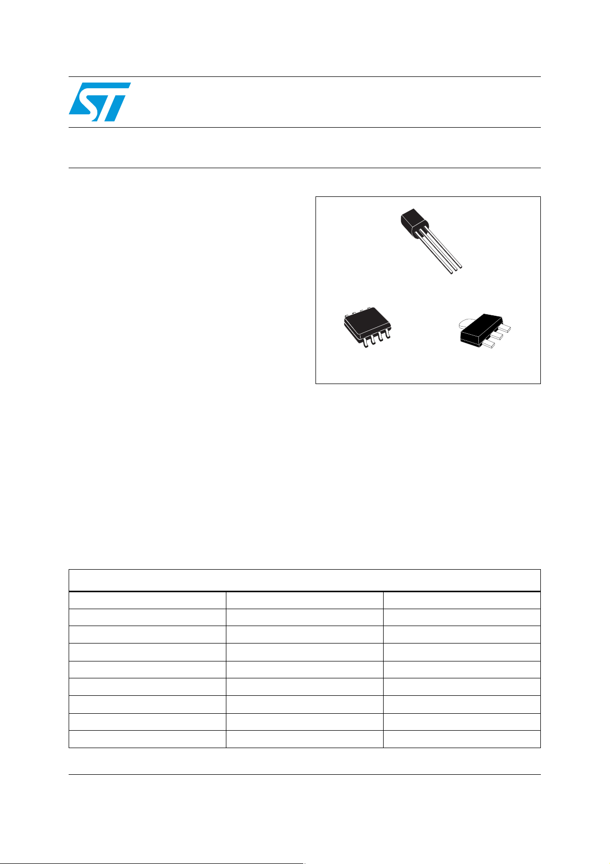
Positive voltage regulators
TO-92
Description
The L78Lxx series of three-terminal positive
regulators employ internal current limiting and
thermal shutdown, making them essentially
indestructible. If adequate heat-sink is provided,
they can deliver up to 100 mA output current.
They are intended as fixed voltage regulators in a
wide range of applications including local or oncard regulation for elimination of noise and
distribution problems associated with single-point
regulation. In addition, they can be used with
power pass elements to make high-current
voltage regulators. The L78Lxx series used as
Zener diode/resistor combination replacement,
offers an effective output impedance improvement
Table 1. Device summary
L78L33C L78L08AC L78L15C
L78L33AC L78L08AB L78L15AC
L78L33AB L78L09C L78L15AB
L78L05C L78L09AC L78L18C
L78L05AC L78L09AB L78L18AC
L78L05AB L78L10AC L78L24C
of typically two orders of magnitude, along with
lower quiescent current and lower noise.
Part numbers
SO-8
SOT-89
L78L06AC L78L12C L78L24AC
L78L06AB L78L12AC L78L24AB
L78L08C L78L12AB
February 2012 Doc ID 2145 Rev 19 1/30
www.st.com
30
Page 2

Contents L78LxxAB - L78LxxAC - L78LxxC
Contents
1 Diagram . . . . . . . . . . . . . . . . . . . . . . . . . . . . . . . . . . . . . . . . . . . . . . . . . . . 3
2 Pin configuration . . . . . . . . . . . . . . . . . . . . . . . . . . . . . . . . . . . . . . . . . . . 4
3 Maximum ratings . . . . . . . . . . . . . . . . . . . . . . . . . . . . . . . . . . . . . . . . . . . . 5
4 Electrical characteristics . . . . . . . . . . . . . . . . . . . . . . . . . . . . . . . . . . . . . 6
5 Typical performance . . . . . . . . . . . . . . . . . . . . . . . . . . . . . . . . . . . . . . . . 16
6 Typical application . . . . . . . . . . . . . . . . . . . . . . . . . . . . . . . . . . . . . . . . . 18
7 Package mechanical data . . . . . . . . . . . . . . . . . . . . . . . . . . . . . . . . . . . . 20
8 Order codes . . . . . . . . . . . . . . . . . . . . . . . . . . . . . . . . . . . . . . . . . . . . . . . 28
9 Revision history . . . . . . . . . . . . . . . . . . . . . . . . . . . . . . . . . . . . . . . . . . . 29
2/30 Doc ID 2145 Rev 19
Page 3
L78LxxAB - L78LxxAC - L78LxxC Diagram
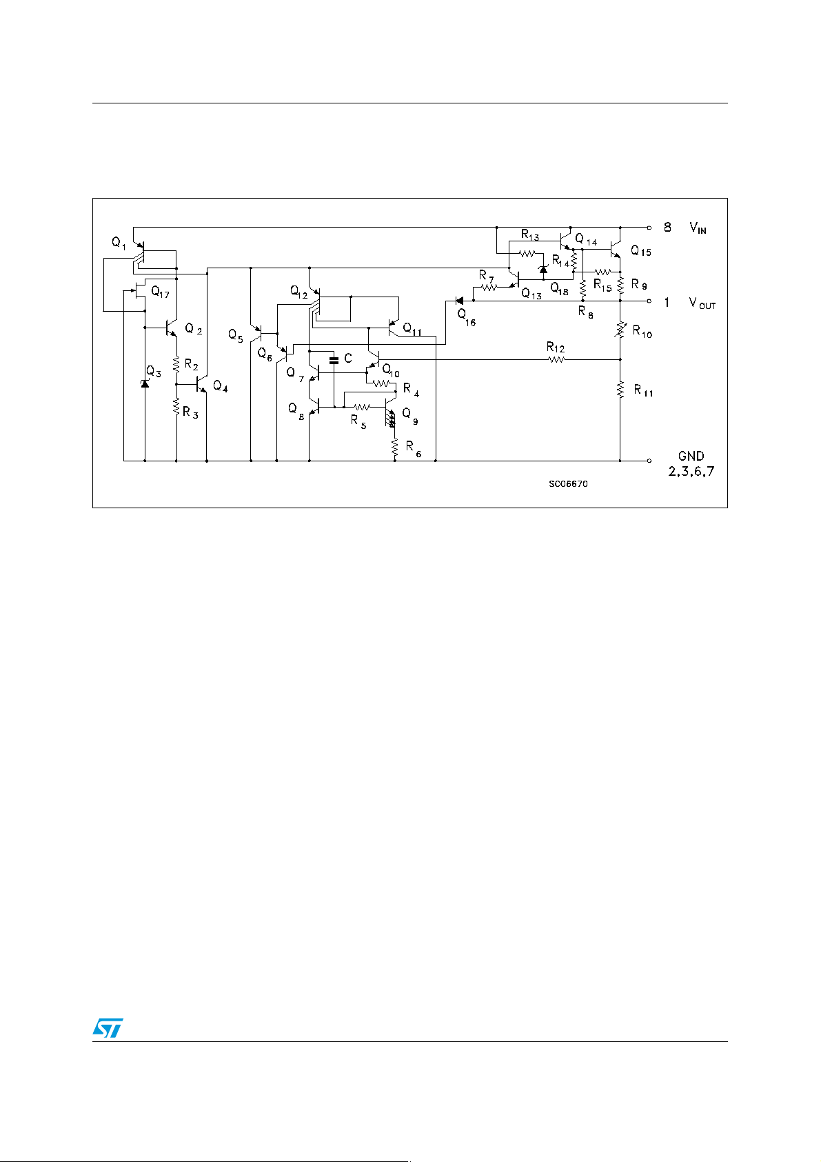
1 Diagram
Figure 1. Schematic diagram
Doc ID 2145 Rev 19 3/30
Page 4
Pin configuration L78LxxAB - L78LxxAC - L78LxxC
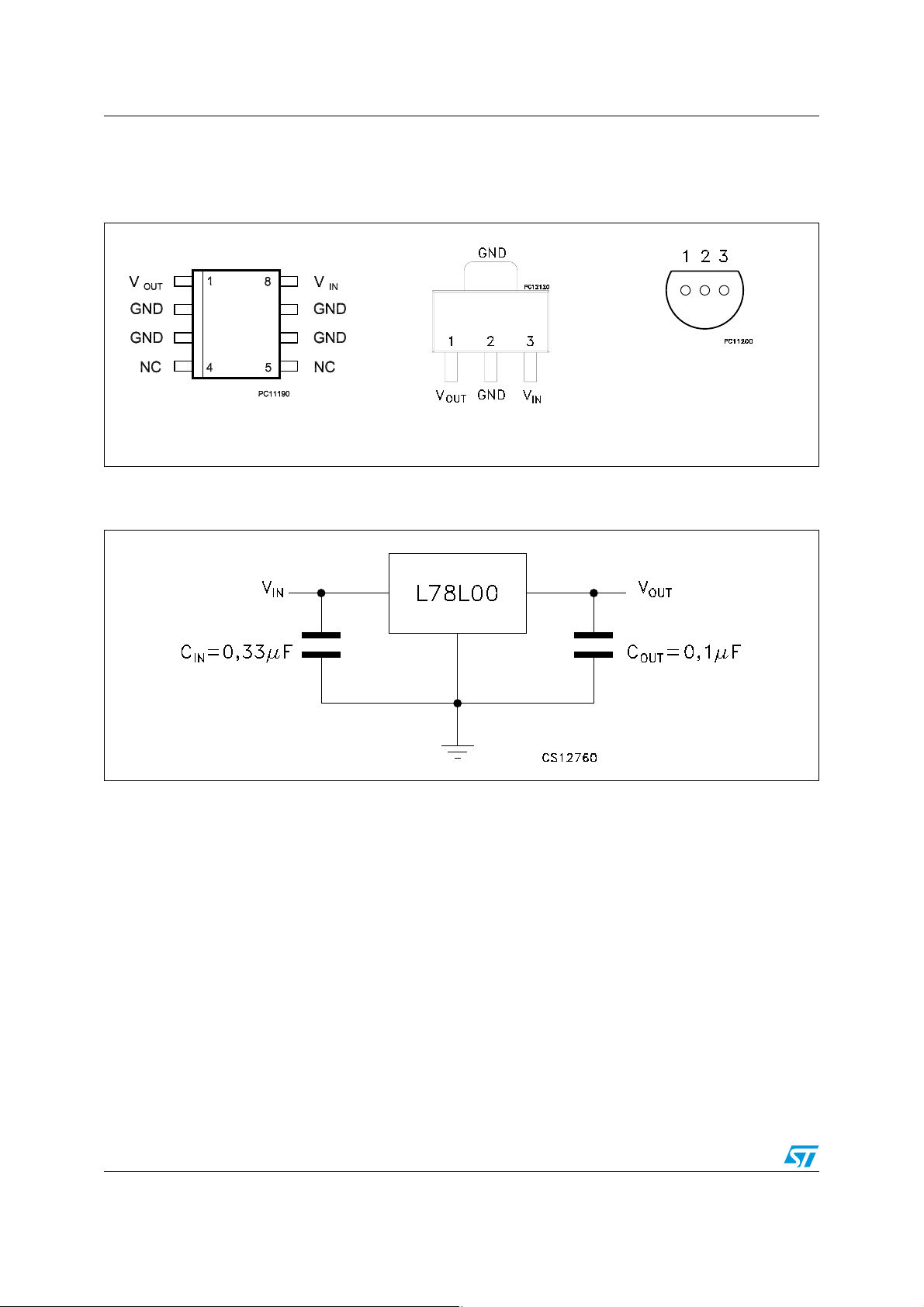
2 Pin configuration
Figure 2. Pin connection (top view, bottom view for TO-92)
SO-8
Figure 3. Test circuits
SOT-89
PIN 1 = V
OUT
PIN 2 = GND
PIN 3 = V
IN
TO-92
4/30 Doc ID 2145 Rev 19
Page 5
L78LxxAB - L78LxxAC - L78LxxC Maximum ratings
3 Maximum ratings
Table 2. Absolute maximum ratings
Symbol Parameter Value Unit
= 3.3 to 9 V 30
V
O
VV
mW
°C
T
V
I
P
STG
DC Input voltage
I
Output current 100 mA
O
Power dissipation Internally limited
D
= 12 to 15 V 35
O
V
= 18 to 24 V 40
O
Storage temperature range -65 to 150 °C
(1)
for L78L00AC 0 to 150
T
OP
1. Our SO-8 package used for voltage regulators is modified internally to have pins 2, 3, 6 and 7 electrically communed to the
die attach flag. This particular frame decreases the total thermal resistance of the package and increases its ability to
dissipate power when an appropriate area of copper on the printed circuit board is available for heat-sinking. The external
dimensions are the same as for the standard SO-8.
Operating junction temperature range
for L78L00AB -40 to 125
Table 3. Thermal data
Symbol Parameter SO-8 TO-92 SOT-89 Unit
R
thJC
R
thJA
1. Considering 6 cm² of copper Board heat-sink.
Thermal resistance junction-case. (max) 20 15 °C/W
Thermal resistance junction-ambient. (max) 55
(1)
200 55
(1)
°C/W
Doc ID 2145 Rev 19 5/30
Page 6
Electrical characteristics L78LxxAB - L78LxxAC - L78LxxC
4 Electrical characteristics
Refer to the test circuits, TJ = 0 to 125 °C, IO = 40 mA, CI = 0.33 µF, CO = 0.1 µF unless
otherwise specified.
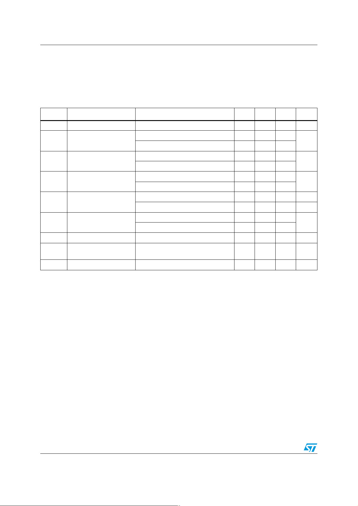
Table 4. Electrical characteristics of L78L33C (VI = 8.3 V)
Symbol Parameter Test conditions Min. Typ. Max. Unit
V
V
ΔV
ΔV
ΔI
Output voltage TJ = 25 °C 3.036 3.3 3.564 V
O
I
= 1 to 40 mA, VI = 5.3 to 20 V 2.97 3.63
Output voltage
O
Line regulation
O
Load regulation
O
I
Quiescent current
d
Quiescent current change
d
O
= 1 to 70 mA, VI = 8.3 V 2.97 3.63
I
O
V
= 5.3 to 20 V, TJ = 25 °C 150
I
= 6.3 to 20 V, TJ = 25 °C 100
V
I
= 1 to 100 mA, TJ = 25 °C 60
I
O
IO = 1 to 40 mA, TJ = 25 °C 30
T
= 25 °C 6 mA
J
T
= 125 °C 5.5 mA
J
I
= 1 to 40 mA 0.2
O
= 6.3 to 20 V 1.5
V
I
eN Output noise voltage B =10 Hz to 100 kHz, T
SVR Supply voltage rejection
V
Dropout voltage 1.7 V
d
VI = 6.3 to 16.3 V, f = 120 Hz
= 40 mA, TJ = 25 °C
I
O
= 25 °C 40 µV
J
41 49 dB
V
mV
mV
mA
6/30 Doc ID 2145 Rev 19
Page 7
L78LxxAB - L78LxxAC - L78LxxC Electrical characteristics
Table 5. Electrical characteristics of L78L05C (VI = 10 V)
Symbol Parameter Test conditions Min. Typ. Max. Unit
V
V
ΔV
ΔV
ΔI
eN Output noise voltage B =10 Hz to 100 kHz, T
SVR Supply voltage rejection
V
Output voltage TJ = 25 °C 4.6 5 5.4 V
O
I
= 1 to 40 mA, VI = 7 to 20 V 4.5 5.5
Output voltage
O
Line regulation
O
Load regulation
O
Quiescent current
I
d
Quiescent current change
d
Dropout voltage 1.7 V
d
O
= 1 to 70 mA, VI = 10 V 4.5 5.5
I
O
= 8.5 to 20 V, TJ = 25 °C 200
V
I
VI = 9 to 20 V, TJ = 25 °C 150
I
= 1 to 100 mA, TJ = 25 °C 60
O
= 1 to 40 mA, TJ = 25 °C 30
I
O
T
= 25 °C 6 mA
J
T
= 125 °C 5.5 mA
J
= 1 to 40 mA 0.2
I
O
VI = 8 to 20 V 1.5
= 25 °C 40 µV
J
= 9 to 20 V, f = 120 Hz
V
I
I
= 40 mA, TJ = 25 °C
O
40 49 dB
V
mV
mV
mA
Table 6. Electrical characteristics of L78L08C (VI = 14 V)
Symbol Parameter Test conditions Min. Typ. Max. Unit
V
V
ΔV
ΔV
ΔI
Output voltage TJ = 25 °C 7.36 8 8.64 V
O
I
= 1 to 40 mA, VI = 8.5 to 20 V 7.2 8.8
Output voltage
O
Line regulation
O
Load regulation
O
Quiescent current
I
d
Quiescent current change
d
O
= 1 to 70 mA, VI = 12 V 7.2 8.8
I
O
V
= 8.5 to 20 V, TJ = 25 °C 200
I
= 9 to 20 V, TJ = 25 °C 150
V
I
I
= 1 to 100 mA, TJ = 25 °C 80
O
= 1 to 40 mA, TJ = 25 °C 40
I
O
T
= 25 °C 6 mA
J
T
= 125 °C 5.5 mA
J
I
= 1 to 40 mA 0.2
O
VI = 8 to 20 V 1.5
eN Output noise voltage B =10 Hz to 100 kHz, T
= 9 to 20 V, f = 120 Hz
V
SVR Supply voltage rejection
V
Dropout voltage 1.7 V
d
I
I
= 40 mA, TJ = 25 °C
O
= 25 °C 60 µV
J
36 45 dB
V
mV
mV
mA
Doc ID 2145 Rev 19 7/30
Page 8
Electrical characteristics L78LxxAB - L78LxxAC - L78LxxC
Table 7. Electrical characteristics of L78L09C (VI = 15 V)
Symbol Parameter Test conditions Min. Typ. Max. Unit
V
V
ΔV
ΔV
ΔI
eN Output noise voltage B =10 Hz to 100 kHz, T
SVR Supply voltage rejection
V
Output voltage TJ = 25 °C 8.28 9 9.72 V
O
I
= 1 to 40 mA, VI = 11.5 to 23 V 8.1 9.9
Output voltage
O
Line regulation
O
Load regulation
O
Quiescent current
I
d
Quiescent current change
d
Dropout voltage 1.7 V
d
O
= 1 to 70 mA, VI = 15 V 8.1 9.9
I
O
= 11.5 to 23 V, TJ = 25 °C 250
V
I
VI = 12 to 23 V, TJ = 25 °C 200
I
= 1 to 100 mA, TJ = 25 °C 80
O
= 1 to 40 mA, TJ = 25 °C 40
I
O
T
= 25 °C 6 mA
J
T
= 125 °C 5.5 mA
J
= 1 to 40 mA 0.2
I
O
VI = 12 to 23 V 1.5
= 25 °C 70 µV
J
= 12 to 23 V, f = 120 Hz
V
I
I
= 40 mA, TJ = 25 °C
O
36 44 dB
V
mV
mV
mA
Table 8. Electrical characteristics of L78L10C (VI = 16 V)
Symbol Parameter Test conditions Min. Typ. Max. Unit
V
V
ΔV
ΔV
ΔI
eN Output noise voltage B =10Hz to 100kHz, TJ = 25 °C 60 µV
SVR Supply voltage rejection
V
Output voltage TJ = 25 °C 9.2 10 10.8 V
O
I
= 1 to 40 mA, VI = 12.5 to 23 V 9 11
Output voltage
O
Line regulation
O
Load regulation
O
I
Quiescent current
d
Quiescent current change
d
Dropout voltage 1.7 V
d
O
IO = 1 to 70 mA, VI = 16 V 9 11
V
= 12.5 to 23 V, TJ = 25 °C 230
I
= 13 to 23 V, TJ = 25 °C 170
V
I
I
= 1 to 100 mA, TJ = 25 °C 80
O
= 1 to 40 mA, TJ = 25 °C 40
I
O
T
= 25 °C 6 mA
J
TJ = 125 °C 5.5 mA
I
= 1 to 40 mA 0.1
O
= 13 to 23 V 1.5
V
I
= 14 to 23 V, f = 120Hz
V
I
= 40 mA, TJ = 25 °C
I
O
V
mV
mV
mA
37 45 dB
8/30 Doc ID 2145 Rev 19
Page 9

L78LxxAB - L78LxxAC - L78LxxC Electrical characteristics
Table 9. Electrical characteristics of L78L12C (VI = 19 V)
Symbol Parameter Test conditions Min. Typ. Max. Unit
V
V
ΔV
ΔV
ΔI
eN Output noise voltage B =10 Hz to 100 kHz, T
SVR Supply voltage rejection
V
Output voltage TJ = 25 °C 11.1 12 12.9 V
O
I
= 1 to 40 mA, VI = 14.5 to 27 V 10.8 13.2
Output voltage
O
Line regulation
O
Load regulation
O
Quiescent current
I
d
Quiescent current change
d
Dropout voltage 1.7 V
d
O
= 1 to 70 mA, VI = 19 V 10.8 13.2
I
O
= 14.5 to 27 V, TJ = 25 °C 250
V
I
VI = 16 to 27 V, TJ = 25 °C 200
I
= 1 to 100 mA, TJ = 25 °C 100
O
= 1 to 40 mA, TJ = 25 °C 50
I
O
T
= 25 °C 6.5 mA
J
T
= 125 °C 6 mA
J
= 1 to 40 mA 0.2
I
O
VI = 16 to 27 V 1.5
= 25 °C 80 µV
J
= 15 to 25 V, f = 120 Hz
V
I
I
= 40 mA, TJ = 25 °C
O
36 42 dB
V
mV
mV
mA
Table 10. Electrical characteristics of L78L15C (VI = 23 V)
Symbol Parameter Test conditions Min. Typ. Max. Unit
V
V
ΔV
ΔV
ΔI
Output voltage TJ = 25 °C 13.8 15 16.2 V
O
I
= 1 to 40 mA, VI = 17.5 to 30 V 13.5 16.5
Output voltage
O
Line regulation
O
Load regulation
O
Quiescent current
I
d
Quiescent current change
d
O
= 1 to 70 mA, VI = 23 V 13.5 16.5
I
O
V
= 17.5 to 30 V, TJ = 25 °C 300
I
= 20 to 30 V, TJ = 25 °C 250
V
I
I
= 1 to 100 mA, TJ = 25 °C 150
O
= 1 to 40 mA, TJ = 25 °C 75
I
O
T
= 25 °C 6.5 mA
J
T
= 125 °C 6 mA
J
I
= 1 to 40 mA 0.2
O
VI = 20 to 30 V 1.5
eN Output noise voltage B =10 Hz to 100 kHz, T
= 18.5 to 28.5 V, f = 120 Hz
V
SVR Supply voltage rejection
V
Dropout voltage 1.7 V
d
I
I
= 40 mA, TJ = 25 °C
O
= 25 °C 90 µV
J
33 39 dB
V
mV
mV
mA
Doc ID 2145 Rev 19 9/30
Page 10

Electrical characteristics L78LxxAB - L78LxxAC - L78LxxC
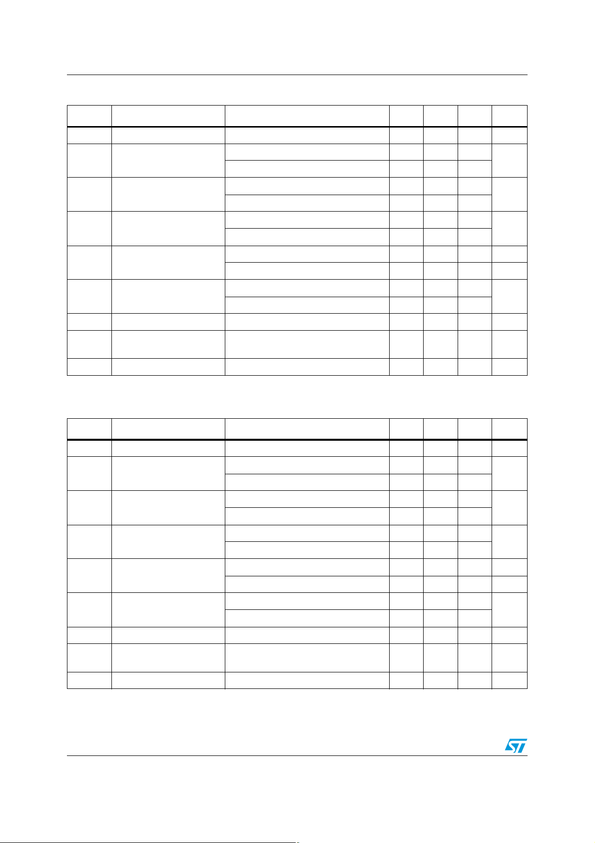
Table 11. Electrical characteristics of L78L18C (VI = 27 V)
Symbol Parameter Test conditions Min. Typ. Max. Unit
V
V
ΔV
ΔV
ΔI
eN Output noise voltage B =10 Hz to 100 kHz, T
SVR Supply voltage rejection
V
Output voltage TJ = 25 °C 16.6 18 19.4 V
O
I
= 1 to 40 mA, VI = 22 to 33 V 16.2 19.8
Output voltage
O
Line regulation
O
Load regulation
O
Quiescent current
I
d
Quiescent current change
d
Dropout voltage 1.7 V
d
O
= 1 to 70 mA, VI = 27 V 16.2 19.8
I
O
= 22 to 33 V, TJ = 25 °C 320
V
I
VI = 22 to 33 V, TJ = 25 °C 270
I
= 1 to 100 mA, TJ = 25 °C 170
O
= 1 to 40 mA, TJ = 25 °C 85
I
O
T
= 25 °C 6.5 mA
J
T
= 125 °C 6 mA
J
= 1 to 40 mA 0.2
I
O
VI = 23 to 33 V 1.5
= 25 °C 120 µV
J
= 23 to 33 V, f = 120 Hz
V
I
I
= 40 mA, TJ = 25 °C
O
32 38 dB
V
mV
mV
mA
Table 12. Electrical characteristics of L78L24C (VI = 33 V)
Symbol Parameter Test conditions Min. Typ. Max. Unit
V
V
ΔV
ΔV
ΔI
Output voltage TJ = 25 °C 22.1 24 25.9 V
O
I
= 1 to 40 mA, VI = 27 to 38 V 21.6 26.4
Output voltage
O
Line regulation
O
Load regulation
O
Quiescent current
I
d
Quiescent current change
d
O
= 1 to 70 mA, VI = 33 V 21.6 26.4
I
O
V
= 27 to 38 V, TJ = 25 °C 350
I
= 28 to 38 V, TJ = 25 °C 300
V
I
I
= 1 to 100 mA, TJ = 25 °C 200
O
= 1 to 40 mA, TJ = 25 °C 100
I
O
T
= 25 °C 6.5 mA
J
T
= 125 °C 6 mA
J
I
= 1 to 40 mA 0.2
O
VI = 28 to 38 V 1.5
eN Output noise voltage B =10 Hz to 100 kHz, T
= 29 to 35 V, f = 120 Hz
V
SVR Supply voltage rejection
V
Dropout voltage 1.7 V
d
I
I
= 40 mA, TJ = 25 °C
O
= 25 °C 200 µV
J
30 37 dB
V
mV
mV
mA
10/30 Doc ID 2145 Rev 19
Page 11

L78LxxAB - L78LxxAC - L78LxxC Electrical characteristics
TJ = 0 to 125 °C for L78L33AC, TJ = -40 to 125 °C for L78L33AB.
Table 13. Electrical characteristics of L78L33AB and L78L33AC (VI = 8.3 V)
Symbol Parameter Test conditions Min. Typ. Max. Unit
V
V
ΔV
ΔV
ΔI
Output voltage TJ = 25 °C 3.168 3.3 3.432 V
O
= 1 to 40 mA, VI = 5.3 to 20 V 3.135 3.465
I
Output voltage
O
Line regulation
O
Load regulation
O
Quiescent current
I
d
Quiescent current change
d
O
IO = 1 to 70 mA, VI = 8.3 V 3.135 3.465
V
= 5.3 to 20 V, TJ = 25 °C 150
I
= 6.3 to 20 V, TJ = 25 °C 100
V
I
I
= 1 to 100 mA, TJ = 25 °C 60
O
= 1 to 40 mA, TJ = 25 °C 30
I
O
= 25 °C 6 mA
T
J
TJ = 125 °C 5.5 mA
I
= 1 to 40 mA 0.1
O
= 6.3 to 20 V 1.5
V
I
eN Output noise voltage B =10 Hz to 100 kHz, TJ = 25 °C 40 µV
= 6.3 to 16.3 V, f = 120 Hz
V
SVR Supply voltage rejection
V
Dropout voltage 1.7 V
d
I
= 40 mA, TJ = 25 °C
I
O
41 49 dB
TJ = 0 to 125 °C for L78L05AC, TJ = -40 to 125 °C for L78L05AB.
Table 14. Electrical characteristics of L78L05AB and L78L05AC (VI = 10 V)
V
mV
mV
mA
Symbol Parameter Test conditions Min. Typ. Max. Unit
V
V
ΔV
ΔV
ΔI
eN Output noise voltage B =10 Hz to 100 kHz, T
SVR Supply voltage rejection
V
Output voltage TJ = 25 °C 4.8 5 5.2 V
O
I
= 1 to 40 mA, VI = 7 to 20 V 4.75 5.25
Output voltage
O
Line regulation
O
Load regulation
O
I
Quiescent current
d
Quiescent current change
d
Dropout voltage 1.7 V
d
O
= 1 to 70 mA, VI = 10 V 4.75 5.25
I
O
V
= 7 to 20 V, TJ = 25 °C 150
I
= 8 to 20 V, TJ = 25 °C 100
V
I
I
= 1 to 100 mA, TJ = 25 °C 60
O
IO = 1 to 40 mA, TJ = 25 °C 30
T
= 25 °C 6 mA
J
T
= 125 °C 5.5 mA
J
I
= 1 to 40 mA 0.1
O
= 8 to 20 V 1.5
V
I
= 25 °C 40 µV
J
VI = 8 to 18 V, f = 120 Hz
= 40 mA, TJ = 25 °C
I
O
41 49 dB
V
mV
mV
mA
Doc ID 2145 Rev 19 11/30
Page 12

Electrical characteristics L78LxxAB - L78LxxAC - L78LxxC
TJ = 0 to 125 °C for L78L06AC, TJ = -40 to 125 °C for L78L06AB.
Table 15. Electrical characteristics of L78L06AB and L78L06AC (VI = 12 V)
Symbol Parameter Test conditions Min. Typ. Max. Unit
V
V
ΔV
ΔV
ΔI
Output voltage TJ = 25 °C 5.76 6 6.24 V
O
= 1 to 40 mA, VI = 8.5 to 20 V 5.7 6.3
I
Output voltage
O
Line regulation
O
Load regulation
O
Quiescent current
I
d
Quiescent current change
d
O
IO = 1 to 70 mA, VI = 12 V 5.7 6.3
V
= 8.5 to 20 V, TJ = 25 °C 150
I
= 9 to 20 V, TJ = 25 °C 100
V
I
I
= 1 to 100 mA, TJ = 25 °C 60
O
= 1 to 40 mA, TJ = 25 °C 30
I
O
= 25 °C 6 mA
T
J
TJ = 125 °C 5.5 mA
I
= 1 to 40 mA 0.1
O
= 9 to 20 V 1.5
V
I
eN Output noise voltage B =10 Hz to 100 kHz, TJ = 25 °C 50 µV
= 9 to 20 V, f = 120 Hz
V
SVR Supply voltage rejection
V
Dropout voltage 1.7 V
d
I
= 40 mA, TJ = 25 °C
I
O
39 46 dB
TJ = 0 to 125 °C for L78L08AC, TJ = -40 to 125 °C for L78L08AB.
Table 16. Electrical characteristics of L78L08AB and L78L08AC (VI = 14 V)
V
mV
mV
mA
Symbol Parameter Test conditions Min. Typ. Max. Unit
V
V
ΔV
ΔV
ΔI
eN Output noise voltage B =10 Hz to 100 kHz, T
SVR Supply voltage rejection
V
Output voltage TJ = 25 °C 7.68 8 8.32 V
O
I
= 1 to 40 mA, VI = 10.5 to 23 V 7.6 8.4
Output voltage
O
Line regulation
O
Load regulation
O
I
Quiescent current
d
Quiescent current change
d
O
= 1 to 70 mA, VI = 14 V 7.6 8.4
I
O
V
= 10.5 to 23 V, TJ = 25 °C 175
I
= 11 to 23 V, TJ = 25 °C 125
V
I
I
= 1 to 100 mA, TJ = 25 °C 80
O
IO = 1 to 40 mA, TJ = 25 °C 40
T
= 25 °C 6 mA
J
T
= 125 °C 5.5 mA
J
I
= 1 to 40 mA 0.1
O
= 11 to 23 V 1.5
V
I
VI = 12 to 23 V, f = 120 Hz
= 40 mA, TJ = 25 °C
I
O
Dropout voltage 1.7 V
d
12/30 Doc ID 2145 Rev 19
= 25 °C 60 µV
J
37 45 dB
V
mV
mV
mA
Page 13

L78LxxAB - L78LxxAC - L78LxxC Electrical characteristics
TJ = 0 to 125 °C for L78L09AC, TJ = -40 to 125 °C for L78L09AB.
Table 17. Electrical characteristics of L78L09AB and L78L09AC (VI = 15 V)
Symbol Parameter Test conditions Min. Typ. Max. Unit
V
V
ΔV
ΔV
ΔI
Output voltage TJ = 25 °C 8.64 9 9.36 V
O
= 1 to 40 mA, VI = 11.5 to 23 V 8.55 9.45
I
Output voltage
O
Line regulation
O
Load regulation
O
Quiescent current
I
d
Quiescent current change
d
O
IO = 1 to 70 mA, VI = 15 V 8.55 9.45
V
= 11.5 to 23 V, TJ = 25 °C 225
I
= 12 to 23 V, TJ = 25 °C 150
V
I
I
= 1 to 100 mA, TJ = 25 °C 80
O
= 1 to 40 mA, TJ = 25 °C 40
I
O
= 25 °C 6 mA
T
J
TJ = 125 °C 5.5 mA
I
= 1 to 40 mA 0.1
O
= 12 to 23 V 1.5
V
I
eN Output noise voltage B =10 Hz to 100 kHz, TJ = 25 °C 70 µV
= 12 to 23 V, f = 120 Hz
V
SVR Supply voltage rejection
V
Dropout voltage 1.7 V
d
I
= 40 mA, TJ = 25 °C
I
O
37 44 dB
TJ = 0 to 125 °C for L78L10AC, TJ = -40 to 125 °C for L78L10AB.
Table 18. Electrical characteristics of L78L10AC (VI = 16 V)
V
mV
mV
mA
Symbol Parameter Test conditions Min. Typ. Max. Unit
V
V
ΔV
ΔV
ΔI
eN Output noise voltage B =10 Hz to 100 kHz, T
SVR Supply voltage rejection
V
Output voltage TJ = 25 °C 9.6 10 10.4 V
O
I
= 1 to 40 mA, VI = 12.5 to 23 V 9.5 10.5
Output voltage
O
Line regulation
O
Load regulation
O
I
Quiescent current
d
Quiescent current change
d
Dropout voltage 1.7 V
d
O
= 1 to 70 mA, VI = 16 V 9.5 10.5
I
O
V
= 12.5 to 23 V, TJ = 25 °C 230
I
= 13 to 23 V, TJ = 25 °C 170
V
I
I
= 1 to 100 mA, TJ = 25 °C 80
O
IO = 1 to 40 mA, TJ = 25 °C 40
T
= 25 °C 6 mA
J
T
= 125 °C 5.5 mA
J
I
= 1 to 40 mA 0.1
O
= 13 to 23 V 1.5
V
I
= 25 °C 60 µV
J
VI = 14 to 23 V, f = 120 Hz
= 40 mA, TJ = 25 °C
I
O
37 45 dB
V
mV
mV
mA
Doc ID 2145 Rev 19 13/30
Page 14

Electrical characteristics L78LxxAB - L78LxxAC - L78LxxC
TJ = 0 to 125 °C for L78L12AC, TJ = -40 to 125 °C for L78L12AB.
Table 19. Electrical characteristics of L78L12AB and L78L12AC (VI = 19 V)
Symbol Parameter Test conditions Min. Typ. Max. Unit
V
V
ΔV
ΔV
ΔI
Output voltage TJ = 25 °C 11.5 12 12.5 V
O
= 1 to 40 mA, VI = 14.5 to 27 V 11.4 12.6
I
Output voltage
O
Line regulation
O
Load regulation
O
Quiescent current
I
d
Quiescent current change
d
O
IO = 1 to 70 mA, VI = 19 V 11.4 12.6
V
= 14.5 to 27 V, TJ = 25 °C 250
I
= 16 to 27 V, TJ = 25 °C 200
V
I
I
= 1 to 100 mA, TJ = 25 °C 100
O
= 1 to 40 mA, TJ = 25 °C 50
I
O
= 25 °C 6.5 mA
T
J
TJ = 125 °C 6 mA
I
= 1 to 40 mA 0.1
O
= 16 to 27 V 1.5
V
I
eN Output noise voltage B =10 Hz to 100 kHz, TJ = 25 °C 80 µV
= 15 to 25 V, f = 120 Hz
V
SVR Supply voltage rejection
V
Dropout voltage 1.7 V
d
I
= 40 mA, TJ = 25 °C
I
O
37 42 dB
TJ = 0 to 125 °C for L78L15AC, TJ = -40 to 125 °C for L78L15AB.
Table 20. Electrical characteristics of L78L15AB and L78L15AC (VI = 23 V)
V
mV
mV
mA
Symbol Parameter Test conditions Min. Typ. Max. Unit
V
V
ΔV
ΔV
ΔI
eN Output noise voltage B =10 Hz to 100 kHz, T
SVR Supply voltage rejection
V
Output voltage TJ = 25 °C 14.4 15 15.6 V
O
I
= 1 to 40 mA, VI = 17.5 to 30 V 14.25 15.75
Output voltage
O
Line regulation
O
Load regulation
O
I
Quiescent current
d
Quiescent current change
d
O
= 1 to 70 mA, VI = 23 V 14.25 15.75
I
O
V
= 17.5 to 30 V, TJ = 25 °C 300
I
= 20 to 30 V, TJ = 25 °C 250
V
I
I
= 1 to 100 mA, TJ = 25 °C 150
O
IO = 1 to 40 mA, TJ = 25 °C 75
T
= 25 °C 6.5 mA
J
T
= 125 °C 6 mA
J
I
= 1 to 40 mA 0.1
O
= 20 to 30 V 1.5
V
I
VI = 18.5 to 28.5 V, f = 120 Hz
= 40 mA, TJ = 25 °C
I
O
Dropout voltage 1.7 V
d
14/30 Doc ID 2145 Rev 19
= 25 °C 90 µV
J
34 39 dB
V
mV
mV
mA
Page 15

L78LxxAB - L78LxxAC - L78LxxC Electrical characteristics
TJ = 0 to 125 °C for L78L18AC, TJ = -40 to 125 °C for L78L18AB.
Table 21. Electrical characteristics of L78L18AC (VI = 27 V)
Symbol Parameter Test conditions Min. Typ. Max. Unit
V
V
ΔV
ΔV
ΔI
Output voltage TJ = 25 °C 17.3 18 18.7 V
O
= 1 to 40 mA, VI = 22 to 33 V 17.1 18.9
I
Output voltage
O
Line regulation
O
Load regulation
O
Quiescent current
I
d
Quiescent current change
d
O
IO = 1 to 70 mA, VI = 27 V 17.1 18.9
V
= 22 to 33 V, TJ = 25 °C 320
I
= 22 to 33 V, TJ = 25 °C 270
V
I
I
= 1 to 100 mA, TJ = 25 °C 170
O
= 1 to 40 mA, TJ = 25 °C 85
I
O
= 25 °C 6.5 mA
T
J
TJ = 125 °C 6 mA
I
= 1 to 40 mA 0.1
O
= 23 to 33 V 1.5
V
I
eN Output noise voltage B =10 Hz to 100 kHz, TJ = 25 °C 120 µV
= 23 to 33 V, f = 120 Hz
V
SVR Supply voltage rejection
V
Dropout voltage 1.7 V
d
I
= 40 mA, TJ = 25 °C
I
O
33 38 dB
TJ = 0 to 125 °C for L78L24AC, TJ = -40 to 125 °C for L78L24AB.
Table 22. Electrical characteristics of L78L24AB and L78L24AC (VI = 33 V)
V
mV
mV
mA
Symbol Parameter Test conditions Min. Typ. Max. Unit
V
V
ΔV
ΔV
ΔI
eN Output noise voltage B =10 Hz to 100 kHz, T
SVR Supply voltage rejection
V
Output voltage TJ = 25 °C 23 24 25 V
O
I
= 1 to 40 mA, VI = 27 to 38 V 22.8 25.2
Output voltage
O
Line regulation
O
Load regulation
O
I
Quiescent current
d
Quiescent current change
d
Dropout voltage 1.7 V
d
O
= 1 to 70 mA, VI = 33 V 22.8 25.2
I
O
V
= 27 to 38 V, TJ = 25 °C 350
I
= 28 to 38 V, TJ = 25 °C 300
V
I
I
= 1 to 100 mA, TJ = 25 °C 200
O
IO = 1 to 40 mA, TJ = 25 °C 100
T
= 25 °C 6.5 mA
J
T
= 125 °C 6 mA
J
I
= 1 to 40 mA 0.1
O
= 28 to 38 V 1.5
V
I
= 25 °C 200 µV
J
VI = 29 to 33 V, f = 120 Hz
= 40 mA, TJ = 25 °C
I
O
31 37 dB
V
mV
mV
mA
Doc ID 2145 Rev 19 15/30
Page 16

Typical performance L78LxxAB - L78LxxAC - L78LxxC
5 Typical performance
Figure 4. L78L05/12 output voltage vs.
ambient temperature
Figure 5. L78L05/12/24 load characteristics
Figure 6. L78L05/12/24 thermal shutdown Figure 7. L78L05/12 quiescent current vs.
output current
Figure 8. L78L05 quiescent current vs. input
16/30 Doc ID 2145 Rev 19
voltage
Figure 9. L78L05/12/24 output characteristics
Page 17

L78LxxAB - L78LxxAC - L78LxxC Typical performance
Figure 10. L78L05/12/24 ripple rejection Figure 11. L78L05 dropout characteristics
Figure 12. L78Lxx short circuit output current
Doc ID 2145 Rev 19 17/30
Page 18

Typical application L78LxxAB - L78LxxAC - L78LxxC
6 Typical application
Figure 13. High output current short circuit protected
Figure 14. Edit boost circuit
Figure 15. Current regulator
18/30 Doc ID 2145 Rev 19
Page 19

L78LxxAB - L78LxxAC - L78LxxC Typical application
Figure 16. Adjustable output regulator
Doc ID 2145 Rev 19 19/30
Page 20

Package mechanical data L78LxxAB - L78LxxAC - L78LxxC
7 Package mechanical data
In order to meet environmental requirements, ST offers these devices in different grades of
®
ECOPACK
specifications, grade definitions and product status are available at:
ECOPACK
packages, depending on their level of environmental compliance. ECOPACK®
®
is an ST trademark.
www.st.com
.
20/30 Doc ID 2145 Rev 19
Page 21

L78LxxAB - L78LxxAC - L78LxxC Package mechanical data
SO-8 mechanical data
Dim.
Min. Typ. Max. Min. Typ. Max.
mm. inch.
A1.35 1.75 0.053 0.069
A1 0.10 0.25 0.04 0.010
A2 1.10 1.65 0.043 0.065
B0.33 0.51 0.013 0.020
C0.19 0.25 0.007 0.010
D4.80 5.00 0.189 0.197
E 3.80 4.00 0.150 0.157
e 1.27 0.050
H5.80 6.20 0.228 0.244
h 0.25 0.50 0.010 0.020
L 0.40 1.27 0.016 0.050
k 8° (max.)
ddd 0.1 0.04
0016023/C
Doc ID 2145 Rev 19 21/30
Page 22

Package mechanical data L78LxxAB - L78LxxAC - L78LxxC
SOT-89 mechanical data
mm. mils.
Dim.
Min. Typ. Max. Min. Typ. Max.
A 1.4 1.6 55.1 63.0
B 0.44 0.56 17.3 22.0
B1 0.36 0.48 14.2 18.9
C0.35 0.44 13.8 17.3
C1 0.35 0.44 13.8 17.3
D 4.4 4.6 173.2 181.1
D1 1.62 1.83 63.8 72.0
E2.29 2.6 90.2 102.4
e 1.42 1.57 55.9 61.8
e1 2.92 3.07 115.0 120.9
H 3.94 4.25 155.1 167.3
L0.89 1.2 35.0 47.2
22/30 Doc ID 2145 Rev 19
P025H
Page 23

L78LxxAB - L78LxxAC - L78LxxC Package mechanical data
TO-92 mechanical data
mm. mils.
Dim.
Min. Typ. Max. Min. Typ. Max.
A4.324.95 170.1 194.9
b 0.36 0.51 14.2 20.1
D 4.45 4.95 175.2 194.9
E 3.30 3.94129.9 155.1
e 2.41 2.67 94.9 105.1
e1 1.14 1.40 44.9 55.1
L 12.7 15.49 500.0 609.8
R 2.16 2.41 85.0 94.9
S10.92 1.52 36.2 59.8
W 0.41 0.56 16.1 22.0
α 5° 5°
0102782/D
Doc ID 2145 Rev 19 23/30
Page 24

Package mechanical data L78LxxAB - L78LxxAC - L78LxxC
Tape & reel SO-8 mechanical data
mm. inch.
Dim.
Min. Typ. Max. Min. Typ. Max.
A 330 12.992
C 12.8 13.2 0.504 0.519
D 20.2 0.795
N60 2.362
T 22.4 0.882
Ao 8.1 8.5 0.319 0.335
Bo 5.5 5.9 0.216 0.232
Ko 2.1 2.3 0.082 0.090
Po 3.9 4.1 0.153 0.161
P7.98.1 0.311 0.319
24/30 Doc ID 2145 Rev 19
Page 25

L78LxxAB - L78LxxAC - L78LxxC Package mechanical data
Tape & reel SOT-89 mechanical data
Dim.
mm. inch.
Min. Typ. Max. Min. Typ. Max.
A180 7.086
C 12.8 13.0 13.2 0.504 0.512 0.519
D 20.2 0.795
N60 2.362
T 14.4 0.567
Ao 4.70 4.804.90 0.185 0.189 0.193
Bo 4.30 4.40 4.50 0.169 0.173 0.177
Ko 1.70 1.801.90 0.067 0.071 0.075
Po 3.9 4.0 4.1 0.153 0.157 0.161
P7.98.0 8.1 0.311 0.315 0.319
Doc ID 2145 Rev 19 25/30
Page 26

Package mechanical data L78LxxAB - L78LxxAC - L78LxxC
Table 23. Tape and reel TO-92 mechanical data
mm. inch.
Dim.
Min. Typ. Max. Min. Typ. Max.
(1)
A1
T
(1)
4.80 0.189
3.80 0.150
T1 1.60 0.063
T2 2.30 0.091
d 0.48 0.019
P0 12.5 12.9 0.492 0.508
P2 5.65 7.05 0.222 0.278
F1, F2 2.44 2.54 2.94 0.096 0.100 0.116
delta H ±2 0.079
W 17.5 18.00 19.0 0.689 0.709 0.748
W0 5.7 6.3 0.224 0.248
W1 8.5 9.25 0.335 0.364
W2 0.50 0.20
H 18.50 18.70 0.728 0.726
H0 15.50 16.50 0.610 0.650
H1 25.00 0.984
D0 3.8 4.2 0.150 0.165
t 0.90 0.035
L1 3 0.118
delta P ±1 0.039
u 50 1.968
Φ1 360 14.173
Φ2 30 1.181
1. For the MAX and MIN values refer to the TO-92 mechanical data
on page 23
.
26/30 Doc ID 2145 Rev 19
Page 27

L78LxxAB - L78LxxAC - L78LxxC Package mechanical data
Figure 17. Tape and reel TO-92 drawing dimension
H1
delta P
A1
T2
T
T1
delta H
H
H0
L
d
W2
l1
W
W0
W1
F1
F2
P2
D0
t
P0
DRAWING NOT IN SCALE
Doc ID 2145 Rev 19 27/30
Page 28

Order codes L78LxxAB - L78LxxAC - L78LxxC
8 Order codes
Table 24. Order codes
Packages
Part numbers
SO-8 TO92 (BAG)
(1)
SOT-89
L78L33C L78L33CD-TR 3.3 V
L78L33AC L78L33ACD13TR L78L33ACZ L78L33ACUTR 3.3 V
L78L33AB L78L33ABD-TR L78L33ABZ L78L33ABUTR 3.3 V
L78L05C L78L05CD13TR L78L05CZ 5 V
L78L05AC L78L05ACD13TR L78L05ACZ L78L05ACUTR 5 V
L78L05AB L78L05ABD13TR L78L05ABZ L78L05ABUTR 5 V
L78L06AC L78L06ACD13TR L78L06ACZ L78L06ACUTR 6 V
L78L06AB L78L06ABD13TR L78L06ABZ L78L06ABUTR 6 V
L78L08C L78L08CD13TR 8 V
L78L08AC L78L08ACD13TR L78L08ACZ L78L08ACUTR 8 V
Output voltages
L78L08AB L78L08ABD13TR L78L08ABZ L78L08ABUTR 8 V
L78L09C L78L09CD13TR 9 V
L78L09AC L78L09ACD13TR L78L09ACZ L78L09ACUTR 9 V
L78L09AB L78L09ABD13TR L78L09ABZ L78L09ABUTR 9 V
L78L10AC L78L10ACUTR 10 V
L78L12C L78L12CD13TR 12 V
L78L12AC L78L12ACD13TR L78L12ACZ L78L12ACUTR 12 V
L78L12AB L78L12ABD-TR L78L12ABZ L78L12ABUTR 12 V
L78L15C L78L15CD-TR 15 V
L78L15AC L78L15ACD13TR L78L15ACZ L78L15ACUTR 15 V
L78L15AB L78L15ABZ L78L15ABUTR 15 V
L78L18C L78L18CD13TR 18 V
L78L18AC L78L18ACUTR 18 V
L78L24C L78L24CD-TR 24 V
L78L24AC L78L24ACZ L78L24ACUTR 24 V
L78L24AB L78L24ABZ 24 V
1. Available in Ammopak with the suffix "-AP" or in tape and reel with the suffix "TR". Please note that in these cases pins are
shaped according to tape and reel specifications.
28/30 Doc ID 2145 Rev 19
Page 29

L78LxxAB - L78LxxAC - L78LxxC Revision history
9 Revision history
Table 25. Document revision history
Date Revision Changes
14-Mar-2005 9 Add tape and reel for TO-92.
15-Mar-2005 10 Add note on Table 3.
23-Dec-2005 11 Mistake on ordering Table in header.
12-Sep-2006 12 Order codes updated.
07-Jun-2007 13 Order codes updated.
18-Sep-2007 14 Added
15-Jul-2008 15 Modified:
18-Aug-2008 16 Modified
03-Apr-2009 17 Added: R
08-Feb-2011 18 Added note
Ta bl e 1
in cover page.
Table 1 on page 1
Figure 12 on page 17
value for SOT-89
thJA
Table 23 on page 26
21-Feb-2012 19 Modified: SOT-89
and
Table 24 on page 28
.
Table 3 on page 5
Figure 2 on page 4
.
.
.
Doc ID 2145 Rev 19 29/30
Page 30

L78LxxAB - L78LxxAC - L78LxxC
Please Read Carefully:
Information in this document is provided solely in connection with ST products. STMicroelectronics NV and its subsidiaries (“ST”) reserve the
right to make changes, corrections, modifications or improvements, to this document, and the products and services described herein at any
time, without notice.
All ST products are sold pursuant to ST’s terms and conditions of sale.
Purchasers are solely responsible for the choice, selection and use of the ST products and services described herein, and ST assumes no
liability whatsoever relating to the choice, selection or use of the ST products and services described herein.
No license, express or implied, by estoppel or otherwise, to any intellectual property rights is granted under this document. If any part of this
document refers to any third party products or services it shall not be deemed a license grant by ST for the use of such third party products
or services, or any intellectual property contained therein or considered as a warranty covering the use in any manner whatsoever of such
third party products or services or any intellectual property contained therein.
UNLESS OTHERWISE SET FORTH IN ST’S TERMS AND CONDITIONS OF SALE ST DISCLAIMS ANY EXPRESS OR IMPLIED
WARRANTY WITH RESPECT TO THE USE AND/OR SALE OF ST PRODUCTS INCLUDING WITHOUT LIMITATION IMPLIED
WARRANTIES OF MERCHANTABILITY, FITNESS FOR A PARTICULAR PURPOSE (AND THEIR EQUIVALENTS UNDER THE LAWS
OF ANY JURISDICTION), OR INFRINGEMENT OF ANY PATENT, COPYRIGHT OR OTHER INTELLECTUAL PROPERTY RIGHT.
UNLESS EXPRESSLY APPROVED IN WRITING BY TWO AUTHORIZED ST REPRESENTATIVES, ST PRODUCTS ARE NOT
RECOMMENDED, AUTHORIZED OR WARRANTED FOR USE IN MILITARY, AIR CRAFT, SPACE, LIFE SAVING, OR LIFE SUSTAINING
APPLICATIONS, NOR IN PRODUCTS OR SYSTEMS WHERE FAILURE OR MALFUNCTION MAY RESULT IN PERSONAL INJURY,
DEATH, OR SEVERE PROPERTY OR ENVIRONMENTAL DAMAGE. ST PRODUCTS WHICH ARE NOT SPECIFIED AS "AUTOMOTIVE
GRADE" MAY ONLY BE USED IN AUTOMOTIVE APPLICATIONS AT USER’S OWN RISK.
Resale of ST products with provisions different from the statements and/or technical features set forth in this document shall immediately void
any warranty granted by ST for the ST product or service described herein and shall not create or extend in any manner whatsoever, any
liability of ST.
ST and the ST logo are trademarks or registered trademarks of ST in various countries.
Information in this document supersedes and replaces all information previously supplied.
The ST logo is a registered trademark of STMicroelectronics. All other names are the property of their respective owners.
© 2012 STMicroelectronics - All rights reserved
Australia - Belgium - Brazil - Canada - China - Czech Republic - Finland - France - Germany - Hong Kong - India - Israel - Italy - Japan -
STMicroelectronics group of companies
Malaysia - Malta - Morocco - Philippines - Singapore - Spain - Sweden - Switzerland - United Kingdom - United States of America
www.st.com
30/30 Doc ID 2145 Rev 19
 Loading...