

现货库存、技术资料、百科信息、热点资讯,精彩尽在鼎好!
Features
■ Output current to 1.5 A
■ Output voltages of 5; 5.2; 6; 8; 8.5; 9; 10; 12;
15; 18; 20; 24 V
■ Thermal overload protection
■ Short circuit protection
■ Output transition SOA protection
Description
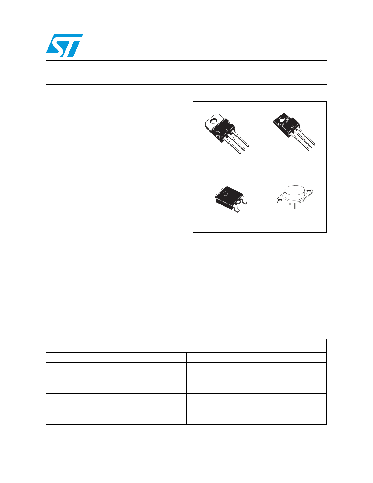
The L78xx series of three-terminal positive
regulators is available in TO-220, TO-220FP,
TO-3 and D
output voltages, making it useful in a wide range
of applications. These regulators can provide
local on-card regulation, eliminating the
distribution problems associated with single point
regulation. Each type employs internal current
limiting, thermal shut-down and safe area
protection, making it essentially indestructible. If
adequate heat sinking is provided, they can
deliver over 1 A output current. Although designed
primarily as fixed voltage regulators, these
devices can be used with external components to
obtain adjustable voltage and currents.
2
PAK packages and several fixed
L78xx
L78xxC
Positive voltage regulators
TO-220
2
D
PAK
TO-220FP
TO-3
Table 1. Device summary
Order codes
L7805 L7810C
L7805C L7812C
L7852C L7815C
L7806C L7818C
L7808C L7820C
L7885C L7824C
L7809C
August 2007 Rev. 16 1/52
www.st.com
52

L78xx - L78xxC
Contents
1 Diagram . . . . . . . . . . . . . . . . . . . . . . . . . . . . . . . . . . . . . . . . . . . . . . . . . . . 5
2 Pin configuration . . . . . . . . . . . . . . . . . . . . . . . . . . . . . . . . . . . . . . . . . . . 6
3 Maximum ratings . . . . . . . . . . . . . . . . . . . . . . . . . . . . . . . . . . . . . . . . . . . . 7
4 Test circuits . . . . . . . . . . . . . . . . . . . . . . . . . . . . . . . . . . . . . . . . . . . . . . . 9
5 Electrical characteristics . . . . . . . . . . . . . . . . . . . . . . . . . . . . . . . . . . . . 11
6 Typical performance . . . . . . . . . . . . . . . . . . . . . . . . . . . . . . . . . . . . . . . . 31
7 Package mechanical data . . . . . . . . . . . . . . . . . . . . . . . . . . . . . . . . . . . . 41
8 Order code . . . . . . . . . . . . . . . . . . . . . . . . . . . . . . . . . . . . . . . . . . . . . . . 50
9 Revision history . . . . . . . . . . . . . . . . . . . . . . . . . . . . . . . . . . . . . . . . . . . 51
2/52

L78xx - L78xxC List of figures
List of figures
Figure 1. Block diagram . . . . . . . . . . . . . . . . . . . . . . . . . . . . . . . . . . . . . . . . . . . . . . . . . . . . . . . . . . . . 5
Figure 2. Pin connections (top view) . . . . . . . . . . . . . . . . . . . . . . . . . . . . . . . . . . . . . . . . . . . . . . . . . . 6
Figure 3. Schematic diagram . . . . . . . . . . . . . . . . . . . . . . . . . . . . . . . . . . . . . . . . . . . . . . . . . . . . . . . . 6
Figure 4. Application circuits . . . . . . . . . . . . . . . . . . . . . . . . . . . . . . . . . . . . . . . . . . . . . . . . . . . . . . . . 8
Figure 5. DC Parameter . . . . . . . . . . . . . . . . . . . . . . . . . . . . . . . . . . . . . . . . . . . . . . . . . . . . . . . . . . . . 9
Figure 6. Load regulation . . . . . . . . . . . . . . . . . . . . . . . . . . . . . . . . . . . . . . . . . . . . . . . . . . . . . . . . . . . 9
Figure 7. Ripple rejection . . . . . . . . . . . . . . . . . . . . . . . . . . . . . . . . . . . . . . . . . . . . . . . . . . . . . . . . . . 10
Figure 8. Dropout voltage vs junction temperature . . . . . . . . . . . . . . . . . . . . . . . . . . . . . . . . . . . . . . 31
Figure 9. Peak output current vs input/output differential voltage . . . . . . . . . . . . . . . . . . . . . . . . . . . 31
Figure 10. Supply voltage rejection vs frequency . . . . . . . . . . . . . . . . . . . . . . . . . . . . . . . . . . . . . . . . 31
Figure 11. Output voltage vs junction temperature . . . . . . . . . . . . . . . . . . . . . . . . . . . . . . . . . . . . . . . 31
Figure 12. Output impedance vs frequency . . . . . . . . . . . . . . . . . . . . . . . . . . . . . . . . . . . . . . . . . . . . . 31
Figure 13. Quiescent current vs junction temp. . . . . . . . . . . . . . . . . . . . . . . . . . . . . . . . . . . . . . . . . . . 31
Figure 14. Load transient response . . . . . . . . . . . . . . . . . . . . . . . . . . . . . . . . . . . . . . . . . . . . . . . . . . . 32
Figure 15. Line transient response . . . . . . . . . . . . . . . . . . . . . . . . . . . . . . . . . . . . . . . . . . . . . . . . . . . 32
Figure 16. Quiescent current vs input voltage . . . . . . . . . . . . . . . . . . . . . . . . . . . . . . . . . . . . . . . . . . . 32
Figure 17. Fixed output regulator . . . . . . . . . . . . . . . . . . . . . . . . . . . . . . . . . . . . . . . . . . . . . . . . . . . . . 32
Figure 18. Current regulator. . . . . . . . . . . . . . . . . . . . . . . . . . . . . . . . . . . . . . . . . . . . . . . . . . . . . . . . . 33
Figure 19. Circuit for increasing output voltage . . . . . . . . . . . . . . . . . . . . . . . . . . . . . . . . . . . . . . . . . . 33
Figure 20. Adjustable output regulator (7 to 30 V) . . . . . . . . . . . . . . . . . . . . . . . . . . . . . . . . . . . . . . . . 33
Figure 21. 0.5 to 10 V Regulator . . . . . . . . . . . . . . . . . . . . . . . . . . . . . . . . . . . . . . . . . . . . . . . . . . . . . 34
Figure 22. High current voltage regulator . . . . . . . . . . . . . . . . . . . . . . . . . . . . . . . . . . . . . . . . . . . . . . 34
Figure 23. High output current with short circuit protection . . . . . . . . . . . . . . . . . . . . . . . . . . . . . . . . . 34
Figure 24. Tracking voltage regulator . . . . . . . . . . . . . . . . . . . . . . . . . . . . . . . . . . . . . . . . . . . . . . . . . 35
Figure 25. Split power supply (± 15 V - 1 A) . . . . . . . . . . . . . . . . . . . . . . . . . . . . . . . . . . . . . . . . . . . . 35
Figure 26. Negative output voltage circuit . . . . . . . . . . . . . . . . . . . . . . . . . . . . . . . . . . . . . . . . . . . . . . 36
Figure 27. Switching regulator . . . . . . . . . . . . . . . . . . . . . . . . . . . . . . . . . . . . . . . . . . . . . . . . . . . . . . . 36
Figure 28. High input voltage circuit. . . . . . . . . . . . . . . . . . . . . . . . . . . . . . . . . . . . . . . . . . . . . . . . . . . 36
Figure 29. High input voltage circuit. . . . . . . . . . . . . . . . . . . . . . . . . . . . . . . . . . . . . . . . . . . . . . . . . . . 37
Figure 30. High output voltage regulator . . . . . . . . . . . . . . . . . . . . . . . . . . . . . . . . . . . . . . . . . . . . . . . 37
Figure 31. High input and output voltage . . . . . . . . . . . . . . . . . . . . . . . . . . . . . . . . . . . . . . . . . . . . . . . 37
Figure 32. Reducing power dissipation with dropping resistor. . . . . . . . . . . . . . . . . . . . . . . . . . . . . . . 38
Figure 33. Remote shutdown . . . . . . . . . . . . . . . . . . . . . . . . . . . . . . . . . . . . . . . . . . . . . . . . . . . . . . . . 38
Figure 34. Power AM modulator (unity voltage gain, I
Figure 35. Adjustable output voltage with temperature compensation . . . . . . . . . . . . . . . . . . . . . . . . 39
Figure 36. Light controllers (V
Figure 37. Protection against input short-circuit with high capacitance loads . . . . . . . . . . . . . . . . . . . 40
Figure 38. Drawing dimension D
Figure 39. Drawing dimension D
Figure 40. D
2
PAK footprint recommended data . . . . . . . . . . . . . . . . . . . . . . . . . . . . . . . . . . . . . . . . . 48
= VXX + VBE) . . . . . . . . . . . . . . . . . . . . . . . . . . . . . . . . . . . . . . . . . 39
Omin
2
PAK (type STD-ST). . . . . . . . . . . . . . . . . . . . . . . . . . . . . . . . . . . . . 45
2
PAK (type WOOSEOK-SUBCON.) . . . . . . . . . . . . . . . . . . . . . . . . . 46
≤ 0.5) . . . . . . . . . . . . . . . . . . . . . . . . . . . . . . . 38
O
3/52

List of tables L78xx - L78xxC
List of tables
Table 1. Device summary . . . . . . . . . . . . . . . . . . . . . . . . . . . . . . . . . . . . . . . . . . . . . . . . . . . . . . . . . . 1
Table 2. Absolute maximum ratings . . . . . . . . . . . . . . . . . . . . . . . . . . . . . . . . . . . . . . . . . . . . . . . . . . 7
Table 3. Thermal data. . . . . . . . . . . . . . . . . . . . . . . . . . . . . . . . . . . . . . . . . . . . . . . . . . . . . . . . . . . . . 7
Table 4. Electrical characteristics of L7805 (refer to the test circuits, T
V
= 10 V, IO = 500 mA, CI = 0.33 µF, CO = 0.1 µF unless otherwise specified) . . . . . . . . 11
I
Table 5. Electrical characteristics of L7806 (refer to the test circuits, T
V
= 11 V,IO = 500 mA, CI = 0.33 µF, CO = 0.1 µF unless otherwise specified) . . . . . . . . . 12
I
Table 6. Electrical characteristics of L7808 (refer to the test circuits, T
V
= 14V, IO = 500 mA, CI = 0.33 µF, CO = 0.1 µF unless otherwise specified) . . . . . . . . . 13
I
Table 7. Electrical characteristics of L7812 (refer to the test circuits, T
V
= 19 V, IO = 500 mA, CI = 0.33 µF, CO = 0.1 µF unless otherwise specified) . . . . . . . . 14
I
Table 8. Electrical characteristics of L7815 (refer to the test circuits, T
V
= 23 V, IO = 500 mA, CI = 0.33 µF, CO = 0.1 µF unless otherwise specified) . . . . . . . . 15
I
Table 9. Electrical characteristics of L7818 (refer to the test circuits, T
V
= 26 V, IO = 500 mA, CI = 0.33 µF, CO = 0.1 µF unless otherwise specified) . . . . . . . . 16
I
Table 10. Electrical characteristics of L7820 (refer to the test circuits, T
V
= 28 V, IO = 500 mA, CI = 0.33 µF, CO = 0.1 µF unless otherwise specified) . . . . . . . . 17
I
Table 11. Electrical characteristics of L7824 (refer to the test circuits, T
V
= 33 V, IO = 500 mA, CI = 0.33 µF, CO = 0.1 µF unless otherwise specified) . . . . . . . . 18
I
Table 12. Electrical characteristics of L7805C (refer to the test circuits, T
V
= 10 V, IO = 500 mA, CI = 0.33 µF, CO = 0.1 µF unless otherwise specified) . . . . . . . . 19
I
Table 13. Electrical characteristics of L7852C (refer to the test circuits, T
V
= 10 V, IO = 500 mA, CI = 0.33 µF, CO = 0.1 µF unless otherwise specified) . . . . . . . . 20
I
Table 14. Electrical characteristics of L7806C (refer to the test circuits, T
V
= 11 V, IO = 500 mA, CI = 0.33 µF, CO = 0.1 µF unless otherwise specified) . . . . . . . . 21
I
Table 15. Electrical characteristics of L7808C (refer to the test circuits, T
V
= 14 V, IO = 500 mA, CI = 0.33 µF, CO = 0.1 µF unless otherwise specified) . . . . . . . . 22
I
Table 16. Electrical characteristics of L7885C (refer to the test circuits, T
V
= 14.5 V, IO = 500 mA, CI = 0.33 µF, CO = 0.1 µF unless otherwise specified) . . . . . . . 23
I
Table 17. Electrical characteristics of L7809C (refer to the test circuits, T
V
= 15 V, IO = 500 mA, CI = 0.33 µF, CO = 0.1 µF unless otherwise specified) . . . . . . . . 24
I
Table 18. Electrical characteristics of L7810C (refer to the test circuits, T
V
= 15 V, IO = 500 mA, CI = 0.33 µF, CO = 0.1 µF unless otherwise specified) . . . . . . . . 25
I
Table 19. Electrical characteristics of L7812C (refer to the test circuits, T
V
= 19 V, IO = 500 mA, CI = 0.33 µF, CO = 0.1 µF unless otherwise specified) . . . . . . . . 26
I
Table 20. Electrical characteristics of L7815C (refer to the test circuits, T
V
= 23 V, IO = 500 mA, CI = 0.33 µF, CO = 0.1 µF unless otherwise specified) . . . . . . . . 27
I
Table 21. Electrical characteristics of L7818C (refer to the test circuits, T
V
= 26 V, IO = 500 mA, CI = 0.33 µF, CO = 0.1 µF unless otherwise specified) . . . . . . . . 28
I
Table 22. Electrical characteristics of L7820C (refer to the test circuits, T
V
= 28 V, IO = 500 mA, CI = 0.33 µF, CO = 0.1 µF unless otherwise specified) . . . . . . . . 29
I
Table 23. Electrical characteristics of L7824C (refer to the test circuits, T
V
= 33 V, IO = 500 mA, CI = 0.33 µF, CO = 0.1 µF unless otherwise specified) . . . . . . . . 30
I
Table 24. D
2
PAK mechanical data . . . . . . . . . . . . . . . . . . . . . . . . . . . . . . . . . . . . . . . . . . . . . . . . . . . 47
Table 25. Footprint data . . . . . . . . . . . . . . . . . . . . . . . . . . . . . . . . . . . . . . . . . . . . . . . . . . . . . . . . . . . 48
Table 26. Order code . . . . . . . . . . . . . . . . . . . . . . . . . . . . . . . . . . . . . . . . . . . . . . . . . . . . . . . . . . . . . 50
Table 27. Revision history . . . . . . . . . . . . . . . . . . . . . . . . . . . . . . . . . . . . . . . . . . . . . . . . . . . . . . . . . 51
= -55 to 150°C,
J
= -55 to 150°C,
J
= -55 to 150°C,
J
= -55 to 150°C,
J
= -55 to 150°C,
J
= -55 to 150°C,
J
= -55 to 150°C,
J
= -55 to 150°C,
J
= 0 to 150°C,
J
= 0 to 150°C,
J
= 0 to 150°C,
J
= 0 to 150°C,
J
= 0 to 150°C,
J
= 0 to 150°C,
J
= 0 to 150°C,
J
= 0 to 150°C,
J
= 0 to 150°C,
J
= 0 to 150°C,
J
= 0 to 150°C,
J
= 0 to 150°C,
J
4/52
L78xx - L78xxC Diagram
1 Diagram
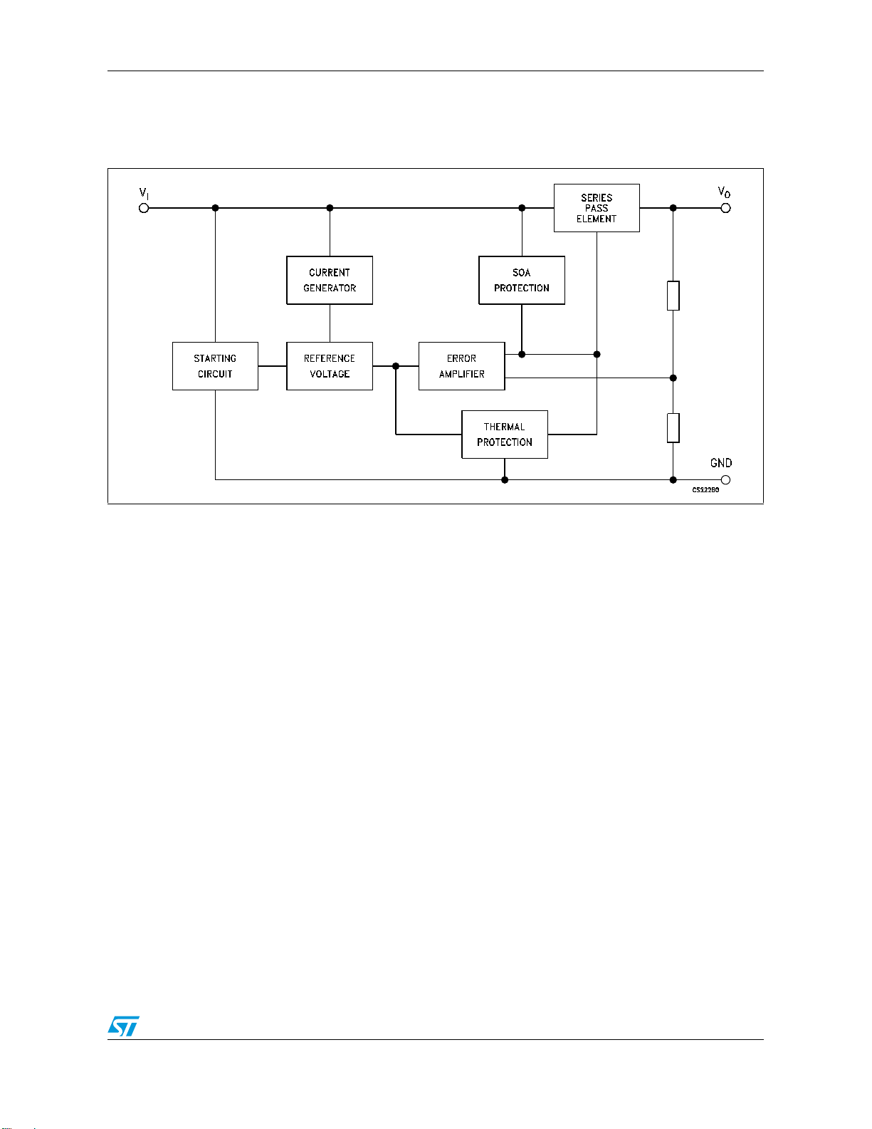
Figure 1. Block diagram
5/52
Pin configuration L78xx - L78xxC
2 Pin configuration
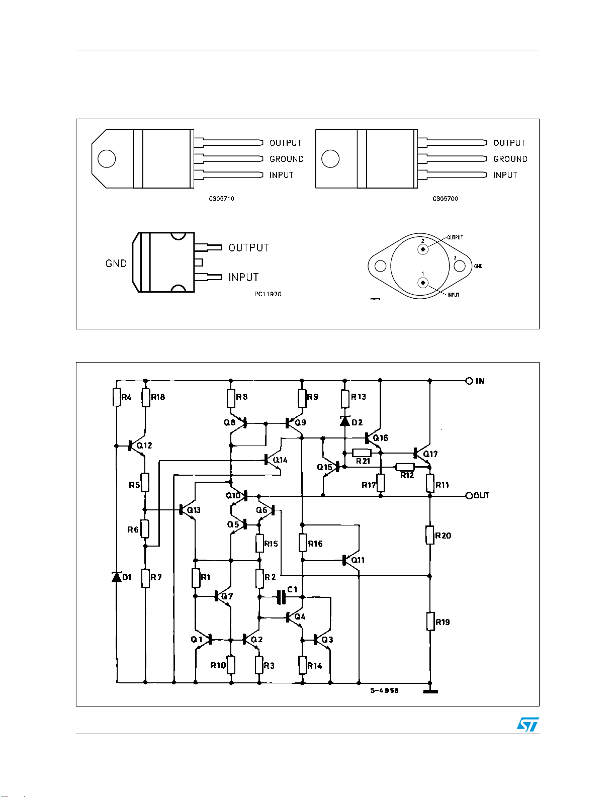
Figure 2. Pin connections (top view)
TO-220
D2PAK (Any Type)
Figure 3. Schematic diagram
TO220FP
TO-3
6/52
L78xx - L78xxC Maximum ratings
3 Maximum ratings
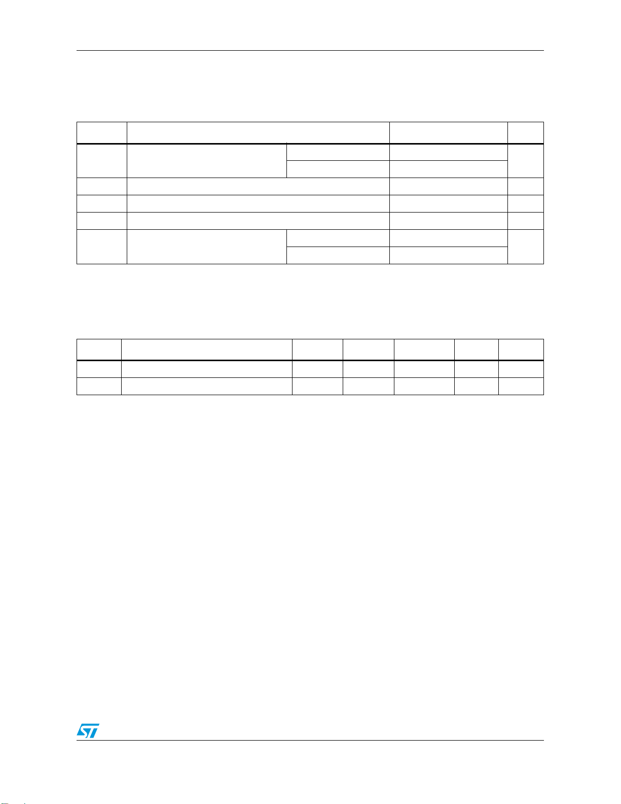
Table 2. Absolute maximum ratings
Symbol Parameter Value Unit
for V
= 5 to 18 V 35
O
= 20, 24 V 40
for V
O
for L7800 -55 to 150
for L7800C 0 to 150
V
°C
T
P
T
V
I
STG
OP
DC Input voltage
I
Output current Internally Limited
O
Power dissipation Internally Limited
D
Storage temperature range -65 to 150 °C
Operating junction temperature range
Note: Absolute Maximum Ratings are those values beyond which damage to the device may
occur. Functional operation under these condition is not implied
Table 3. Thermal data
Symbol Parameter D2PAK TO-220 TO-220FP TO-3 Unit
R
R
Thermal resistance junction-case 3 5 5 4 °C/W
thJC
Thermal resistance junction-ambient 62.5 50 60 35 °C/W
thJA
7/52
Maximum ratings L78xx - L78xxC
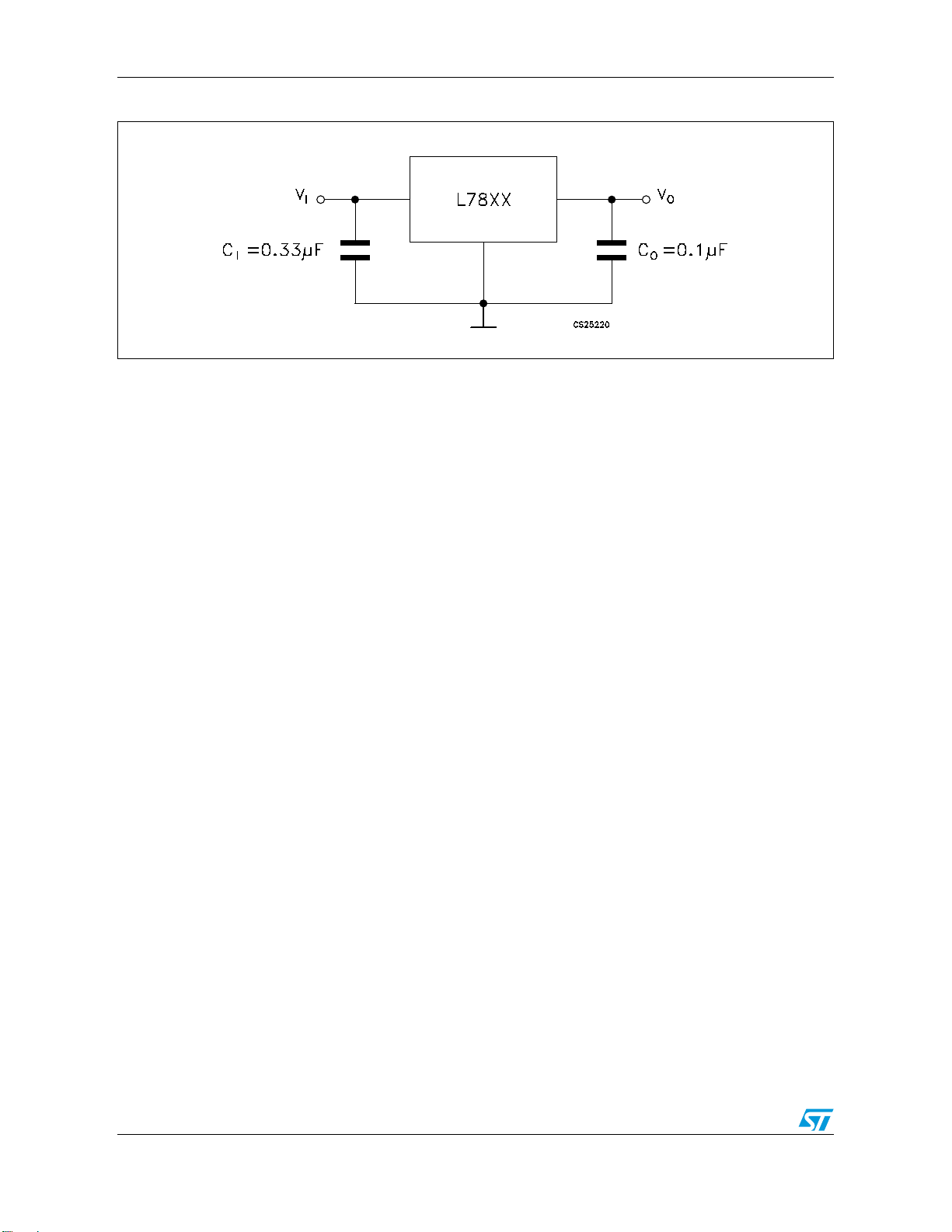
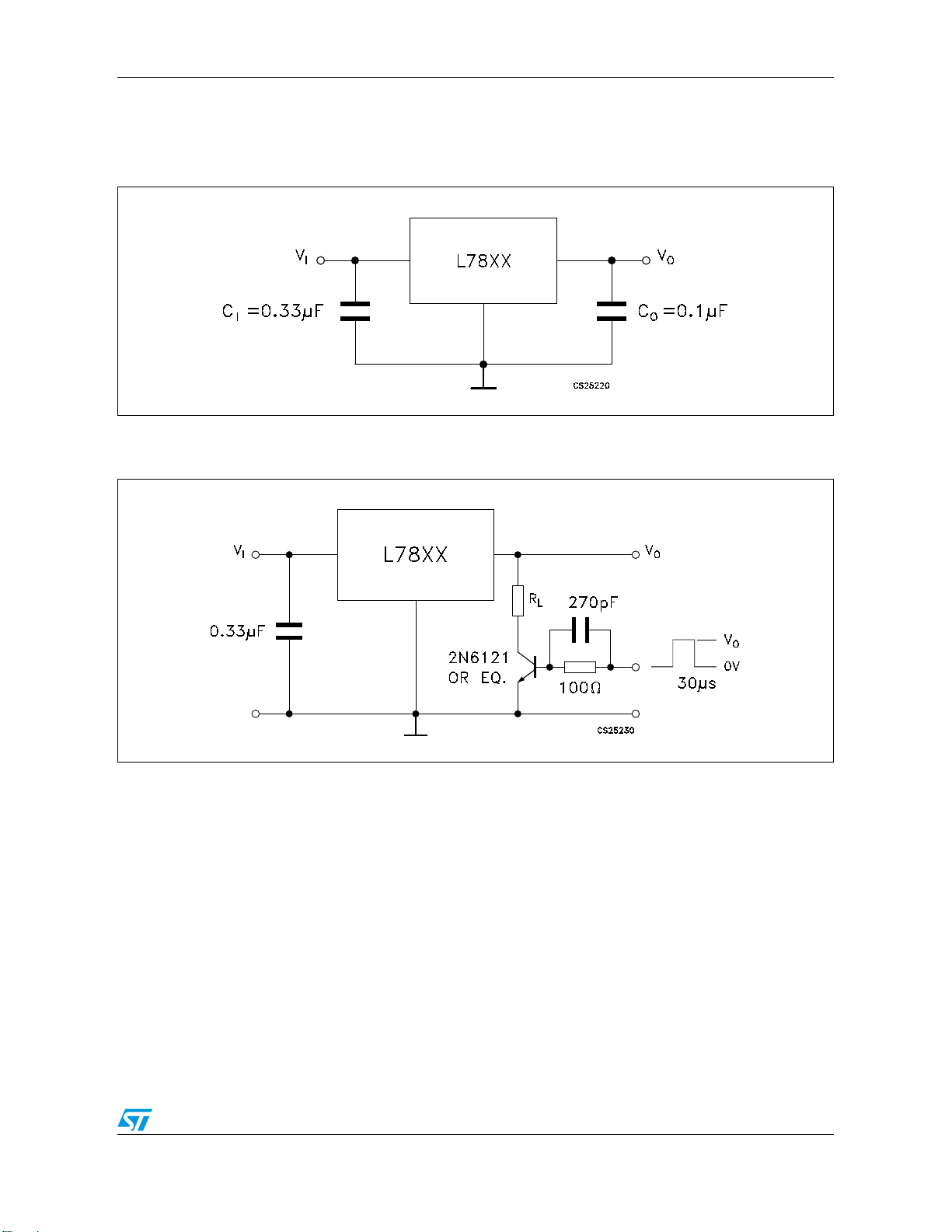
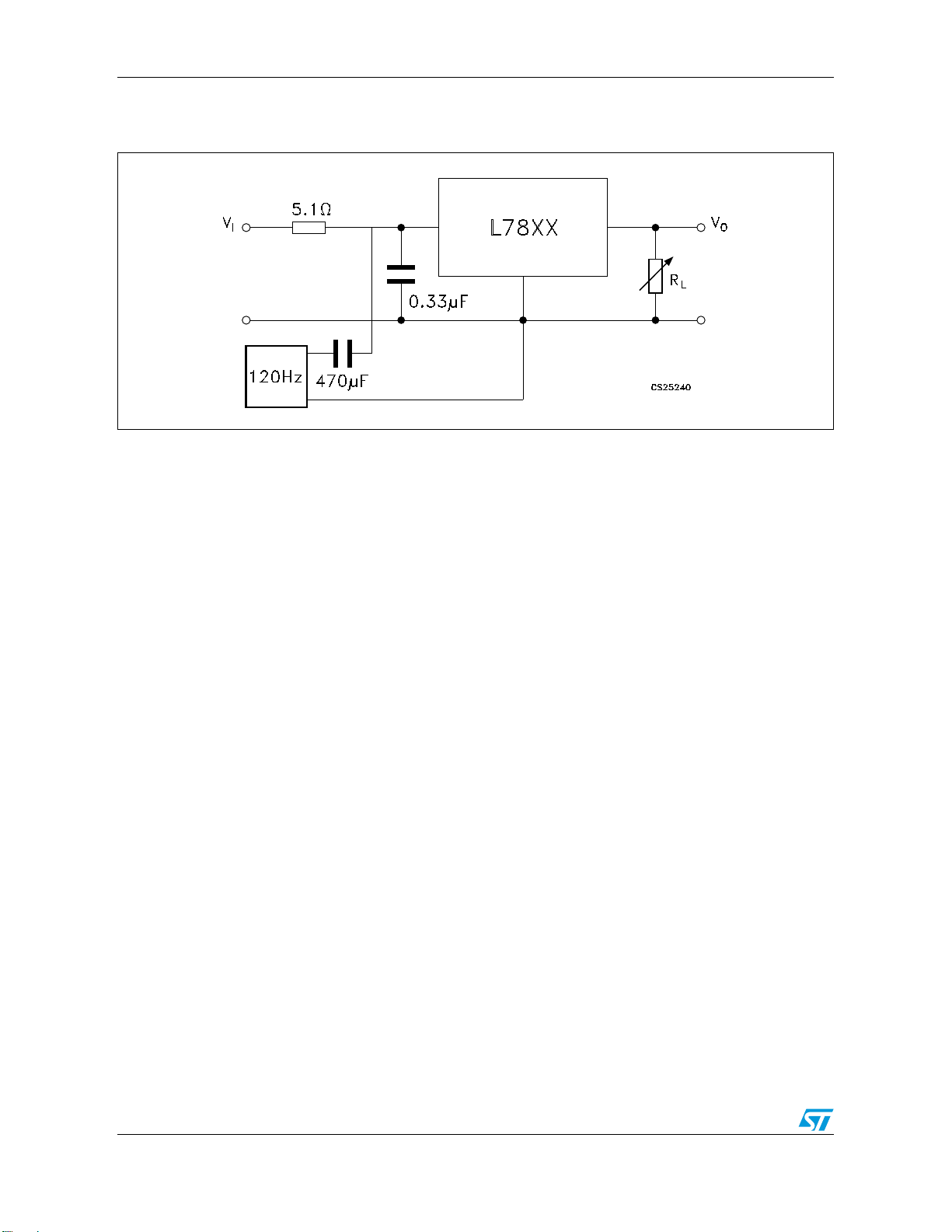
Figure 4. Application circuits
8/52
L78xx - L78xxC Test circuits
4 Test circuits
Figure 5. DC Parameter
Figure 6. Load regulation
9/52
Test circuits L78xx - L78xxC
Figure 7. Ripple rejection
10/52
L78xx - L78xxC Electrical characteristics
5 Electrical characteristics
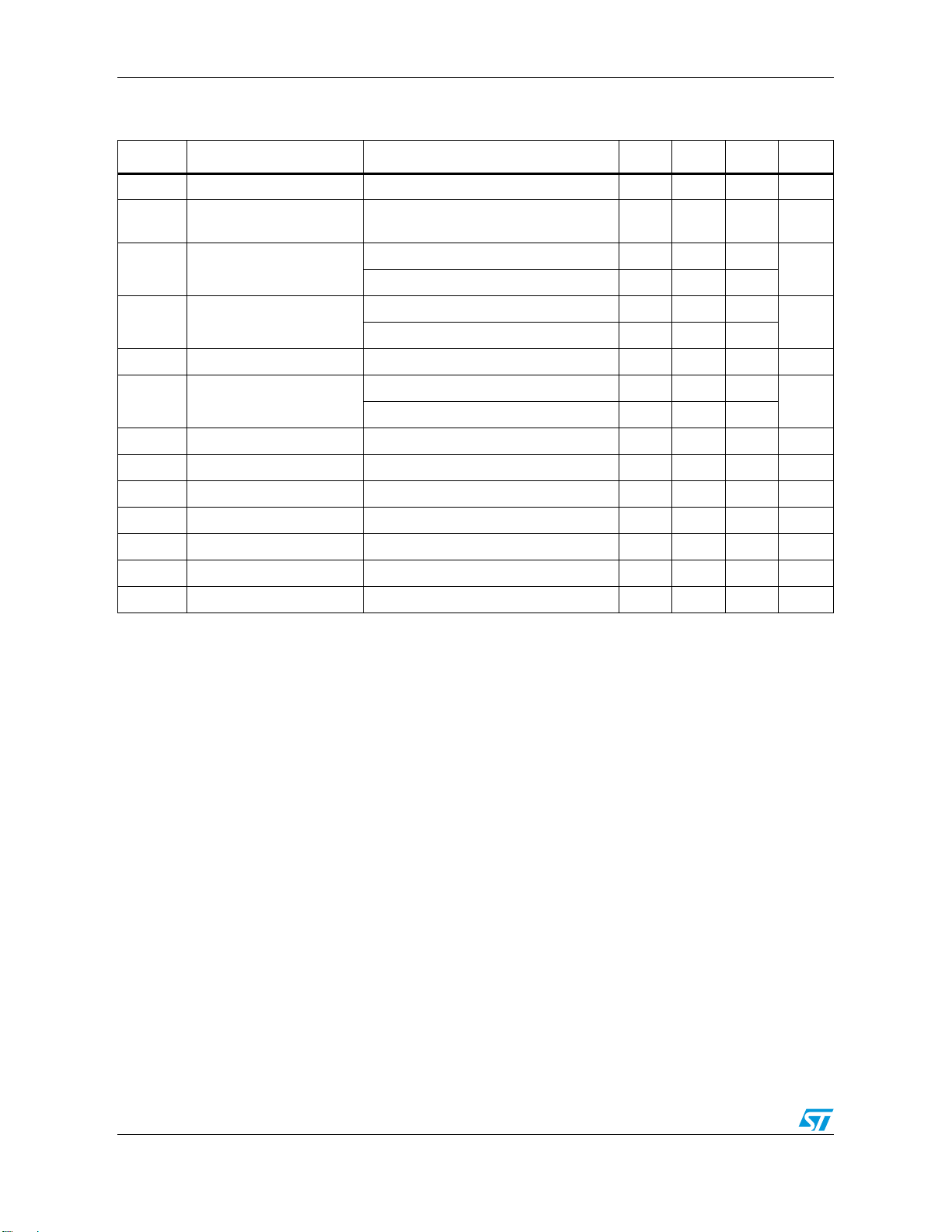
Table 4. Electrical characteristics of L7805 (refer to the test circuits, TJ = -55 to 150°C, VI = 10 V,
I
= 500 mA, CI = 0.33 µF, CO = 0.1 µF unless otherwise specified)
O
Symbol Parameter Test conditions Min. Typ. Max. Unit
V
V
ΔV
ΔV
Output voltage TJ = 25°C 4.8 5 5.2 V
O
= 5 mA to 1 A, PO ≤ 15 W
I
Output voltage
O
(1)
Line regulation
O
(1)
Load regulation
O
Quiescent current TJ = 25°C 6 mA
I
d
O
= 8 to 20 V
V
I
V
= 7 to 25 V, TJ = 25°C 3 50
I
= 8 to 12 V, TJ = 25°C 1 25
V
I
I
= 5 mA to 1.5 A, TJ = 25°C 100
O
= 250 to 750 mA, TJ = 25°C 25
I
O
4.65 5 5.35 V
IO = 5 mA to 1 A 0.5
ΔI
ΔV
eN Output noise voltage B =10 Hz to 100 KHz, T
Quiescent current change
d
/ΔT Output voltage drift IO = 5 mA 0.6 mV/°C
O
= 8 to 25 V 0.8
V
I
= 25°C 40 µV/V
J
SVR Supply voltage rejection VI = 8 to 18 V, f = 120 Hz 68 dB
V
R
I
I
1. Load and line regulation are specified at constant junction temperature. Changes in VO due to heating effects must be
taken into account separately. Pulse testing with low duty cycle is used.
Dropout voltage IO = 1 A, TJ = 25°C 2 2.5 V
d
Output resistance f = 1 KHz 17 mΩ
O
Short circuit current VI = 35 V, TJ = 25°C 0.75 1.2 A
sc
Short circuit peak current TJ = 25°C 1.3 2.2 3.3 A
scp
mV
mV
mA
O
11/52
Electrical characteristics L78xx - L78xxC
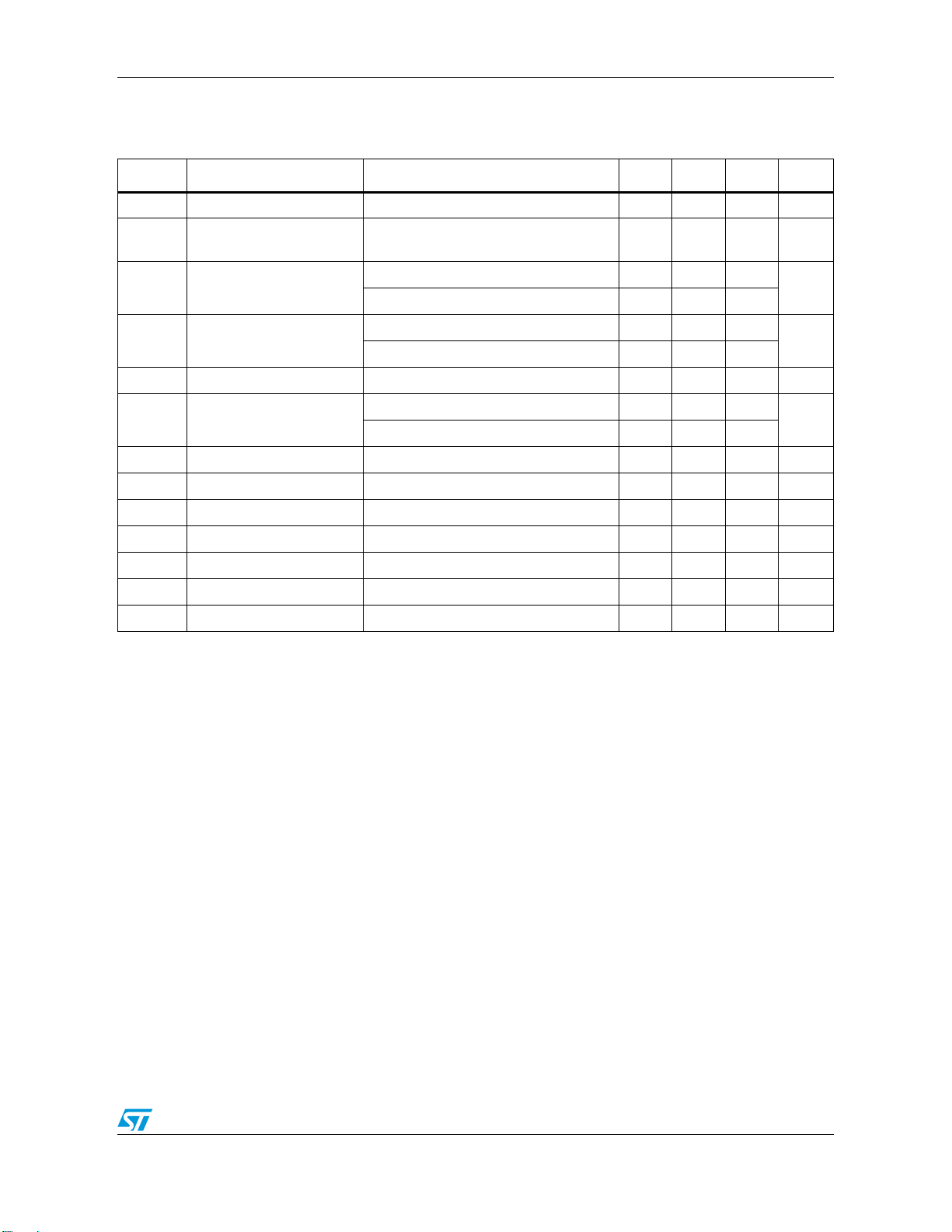
Table 5. Electrical characteristics of L7806 (refer to the test circuits, TJ = -55 to 150°C, VI = 11 V,
I
= 500 mA, CI = 0.33 µF, CO = 0.1 µF unless otherwise specified)
O
Symbol Parameter Test conditions Min. Typ. Max. Unit
V
V
ΔV
ΔV
ΔI
ΔV
eN Output noise voltage B =10 Hz to 100 KHz, T
Output voltage TJ = 25°C 5.75 6 6.25 V
O
= 5 mA to 1 A, PO ≤ 15 W
I
Output voltage
O
(1)
Line regulation
O
(1)
Load regulation
O
Quiescent current TJ = 25°C 6 mA
I
d
Quiescent current change
d
/ΔT Output voltage drift IO = 5 mA 0.7 mV/°C
O
O
= 9 to 21 V
V
I
V
= 8 to 25 V, TJ = 25°C 60
I
= 9 to 13 V, TJ = 25°C 30
V
I
I
= 5 mA to 1.5 A, TJ = 25°C 100
O
= 250 to 750 mA, TJ = 25°C 30
I
O
I
= 5 mA to 1 A 0.5
O
= 9 to 25 V 0.8
V
I
= 25°C 40 µV/V
J
5.65 6 6.35 V
SVR Supply voltage rejection VI = 9 to 19 V, f = 120 Hz 65 dB
V
R
I
I
1. Load and line regulation are specified at constant junction temperature. Changes in VO due to heating effects must be
taken into account separately. Pulse testing with low duty cycle is used.
Dropout voltage IO = 1 A, TJ = 25°C 2 2.5 V
d
Output resistance f = 1 KHz 19 mΩ
O
Short circuit current VI = 35 V, TJ = 25°C 0.75 1.2 A
sc
Short circuit peak current TJ = 25°C 1.3 2.2 3.3 A
scp
mV
mV
mA
O
12/52
L78xx - L78xxC Electrical characteristics
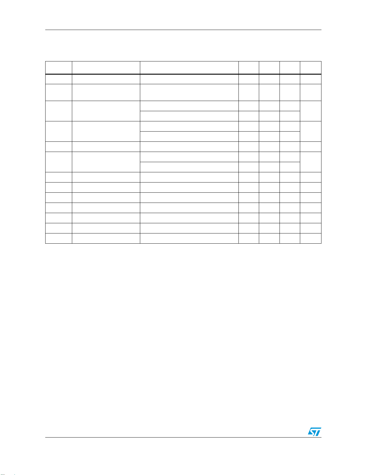
Table 6. Electrical characteristics of L7808 (refer to the test circuits, TJ = -55 to 150°C, VI = 14V, IO
= 500 mA, C
Symbol Parameter Test conditions Min. Typ. Max. Unit
= 0.33 µF, CO = 0.1 µF unless otherwise specified)
I
V
V
ΔV
ΔV
ΔI
ΔV
eN Output noise voltage B =10 Hz to 100 KHz, T
Output voltage TJ = 25°C 7.7 8 8.3 V
O
= 5 mA to 1A, PO ≤ 15 W
I
Output voltage
O
(1)
Line regulation
O
(1)
Load regulation
O
Quiescent current TJ = 25°C 6 mA
I
d
Quiescent current change
d
/ΔT Output voltage drift IO = 5 mA 1 mV/°C
O
O
= 11.5 to 23 V
V
I
V
= 10.5 to 25 V, TJ = 25°C 80
I
= 11 to 17 V, TJ = 25°C 40
V
I
I
= 5 mA to 1.5 A, TJ = 25°C 100
O
= 250 to 750 mA, TJ = 25°C 40
I
O
I
= 5 mA to 1 A 0.5
O
= 11.5 to 25 V 0.8
V
I
= 25°C 40 µV/V
J
7.6 8 8.4 V
SVR Supply voltage rejection VI = 11.5 to 21.5 V, f = 120 Hz 62 dB
V
R
I
I
1. Load and line regulation are specified at constant junction temperature. Changes in VO due to heating effects must be
taken into account separately. Pulse testing with low duty cycle is used.
Dropout voltage IO = 1 A, TJ = 25°C 2 2.5 V
d
Output resistance f = 1 KHz 16 mΩ
O
Short circuit current VI = 35 V, TJ = 25°C 0.75 1.2 A
sc
Short circuit peak current TJ = 25°C 1.3 2.2 3.3 A
scp
mV
mV
mA
O
13/52
Electrical characteristics L78xx - L78xxC
Table 7. Electrical characteristics of L7812 (refer to the test circuits, TJ = -55 to 150°C, VI = 19 V,
I
= 500 mA, CI = 0.33 µF, CO = 0.1 µF unless otherwise specified)
O
Symbol Parameter Test conditions Min. Typ. Max. Unit
V
V
ΔV
ΔV
ΔI
ΔV
eN Output noise voltage B =10 Hz to 100 KHz, T
Output voltage TJ = 25°C 11.5 12 12.5 V
O
= 5 mA to 1 A, PO ≤ 15 W
I
Output voltage
O
(1)
Line regulation
O
(1)
Load regulation
O
Quiescent current TJ = 25°C 6 mA
I
d
Quiescent current change
d
/ΔT Output voltage drift IO = 5 mA 1.5 mV/°C
O
O
= 15.5 to 27 V
V
I
V
= 14.5 to 30 V, TJ = 25°C 120
I
= 16 to 22 V, TJ = 25°C 60
V
I
I
= 5 mA to 1.5 A, TJ = 25°C 100
O
= 250 to 750 mA, TJ = 25°C 60
I
O
I
= 5 mA to 1 A 0.5
O
= 15 to 30 V 0.8
V
I
= 25°C 40 µV/V
J
11.4 12 12.6 V
SVR Supply voltage rejection VI = 15 to 25 V, f = 120 Hz 61 dB
V
R
I
I
1. Load and line regulation are specified at constant junction temperature. Changes in VO due to heating effects must be
taken into account separately. Pulse testing with low duty cycle is used.
Dropout voltage IO = 1 A, TJ = 25°C 2 2.5 V
d
Output resistance f = 1 KHz 18 mΩ
O
Short circuit current VI = 35 V, TJ = 25°C 0.75 1.2 A
sc
Short circuit peak current TJ = 25°C 1.3 2.2 3.3 A
scp
mV
mV
mA
O
14/52

L78xx - L78xxC Electrical characteristics
Table 8. Electrical characteristics of L7815 (refer to the test circuits, TJ = -55 to 150°C, VI = 23 V,
I
= 500 mA, CI = 0.33 µF, CO = 0.1 µF unless otherwise specified)
O
Symbol Parameter Test conditions Min. Typ. Max. Unit
V
V
ΔV
ΔV
ΔI
ΔV
eN Output noise voltage B =10 Hz to 100 KHz, T
Output voltage TJ = 25°C 14.4 15 15.6 V
O
= 5 mA to 1 A, PO ≤ 15 W
I
Output voltage
O
(1)
Line regulation
O
(1)
Load regulation
O
Quiescent current TJ = 25°C 6 mA
I
d
Quiescent current change
d
/ΔT Output voltage drift IO = 5 mA 1.8 mV/°C
O
O
= 18.5 to 30 V
V
I
V
= 17.5 to 30 V, TJ = 25°C 150
I
= 20 to 26 V, TJ = 25°C 75
V
I
I
= 5 mA to 1.5 A, TJ = 25°C 150
O
= 250 to 750 mA, TJ = 25°C 75
I
O
I
= 5 mA to 1 A 0.5
O
= 18.5 to 30 V 0.8
V
I
= 25°C 40 µV/V
J
14.25 15 15.75 V
SVR Supply voltage rejection VI = 18.5 to 28.5 V, f = 120 Hz 60 dB
V
R
I
I
1. Load and line regulation are specified at constant junction temperature. Changes in VO due to heating effects must be
taken into account separately. Pulse testing with low duty cycle is used.
Dropout voltage IO = 1 A, TJ = 25°C 2 2.5 V
d
Output resistance f = 1 KHz 19 mΩ
O
Short circuit current VI = 35 V, TJ = 25°C 0.75 1.2 A
sc
Short circuit peak current TJ = 25°C 1.3 2.2 3.3 A
scp
mV
mV
mA
O
15/52

Electrical characteristics L78xx - L78xxC
Table 9. Electrical characteristics of L7818 (refer to the test circuits, TJ = -55 to 150°C, VI = 26 V,
I
= 500 mA, CI = 0.33 µF, CO = 0.1 µF unless otherwise specified)
O
Symbol Parameter Test conditions Min. Typ. Max. Unit
V
V
ΔV
ΔV
ΔI
ΔV
eN Output noise voltage B =10 Hz to 100 KHz, T
Output voltage TJ = 25°C 17.3 18 18.7 V
O
= 5 mA to 1 A, PO ≤ 15 W
I
Output voltage
O
(1)
Line regulation
O
(1)
Load regulation
O
Quiescent current TJ = 25°C 6 mA
I
d
Quiescent current change
d
/ΔT Output voltage drift IO = 5 mA 2.3 mV/°C
O
O
= 22 to 33 V
V
I
V
= 21 to 33 V, TJ = 25°C 180
I
= 24 to 30 V, TJ = 25°C 90
V
I
I
= 5 mA to 1.5 A, TJ = 25°C 180
O
= 250 to 750 mA, TJ = 25°C 90
I
O
I
= 5 mA to 1 A 0.5
O
= 22 to 33 V 0.8
V
I
= 25°C 40 µV/V
J
17.1 18 18.9 V
SVR Supply voltage rejection VI = 22 to 32 V, f = 120 Hz 59 dB
V
R
I
I
1. Load and line regulation are specified at constant junction temperature. Changes in VO due to heating effects must be
taken into account separately. Pulse testing with low duty cycle is used.
Dropout voltage IO = 1 A, TJ = 25°C 2 2.5 V
d
Output resistance f = 1 KHz 22 mΩ
O
Short circuit current VI = 35 V, TJ = 25°C 0.75 1.2 A
sc
Short circuit peak current TJ = 25°C 1.3 2.2 3.3 A
scp
mV
mV
mA
O
16/52
 Loading...