

现货库存、技术资料、百科信息、热点资讯,精彩尽在鼎好!
Feature summary
■ Output current in excess of 1A
■ Output voltages of 5; 6; 8; 9; 12; 15; 18; 20; 24V
■ Thermal overload protection
■ Output transition SOA protection
■ 2% Output voltage tolerance
■ Guaranteed in extended temperature range
L7800AB/AC series
Precision 1A regulators
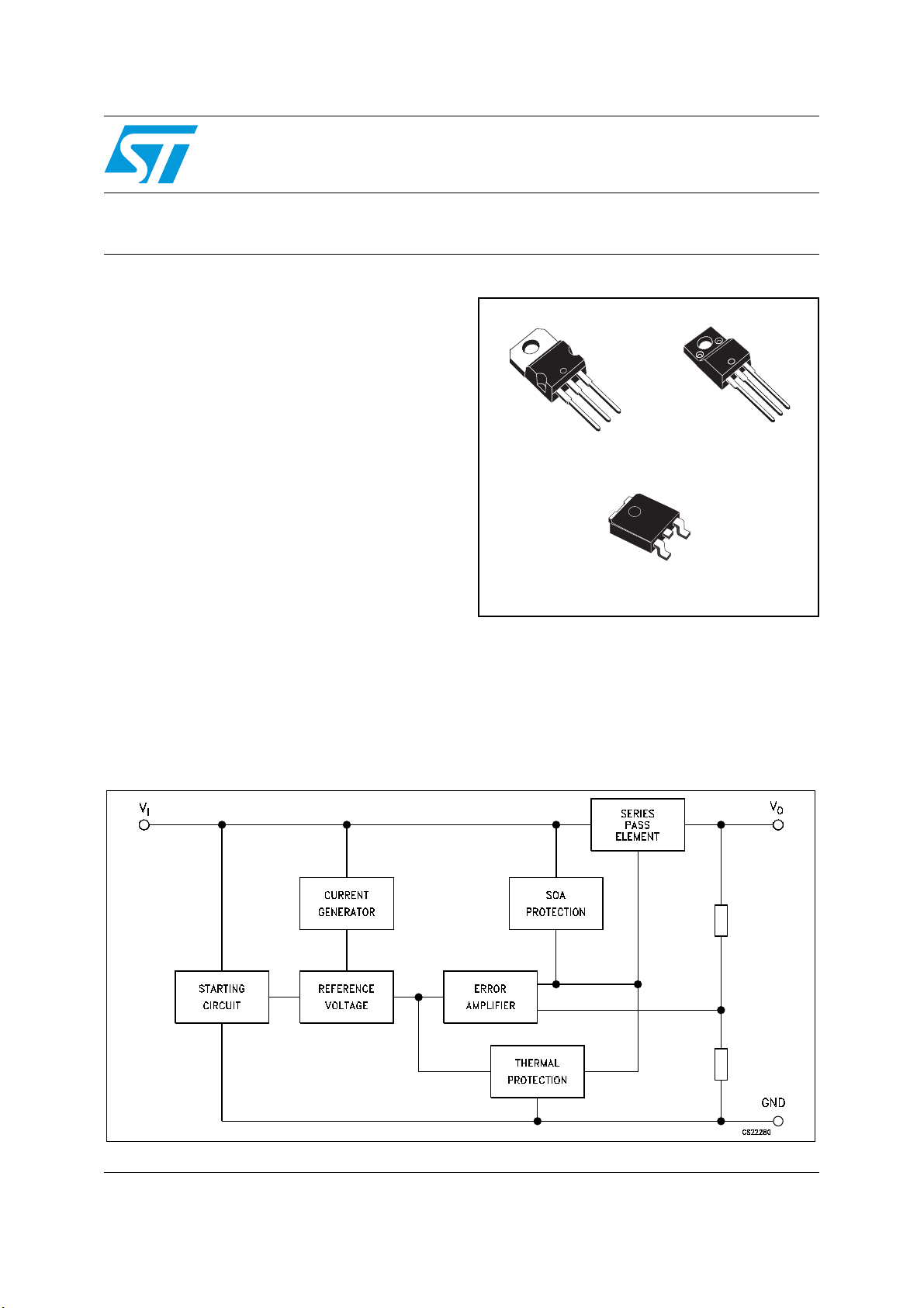
TO-220
TO-220FP
Description
The L7800A series of three terminal positive
regulators is available in TO-220, TO-220FP, and
2
D
PAK packages and several fixed output
voltages, making it useful in a wide range of
applications. These regulators can provide local
on-card regulation, eliminating the distribution
problem associated with single point regulation.
Each type employs internal current limiting,
thermal shut-down and safe area protection,
making it essentially indestructible. If adequate
heat sinking is provided, they can
Schematic diagram
D2PAK
deliver over 1A output current, Although designed
primarily as fixed voltage regulators, these
devices can be used with external components to
obtain adjustable voltage and currents.
January 2007 Rev. 11 1/28
www.st.com
28

L7800AB/AC series
Contents
1 Pin configuration . . . . . . . . . . . . . . . . . . . . . . . . . . . . . . . . . . . . . . . . . . . 3
2 Maximum ratings . . . . . . . . . . . . . . . . . . . . . . . . . . . . . . . . . . . . . . . . . . . . 4
3 Test circuits . . . . . . . . . . . . . . . . . . . . . . . . . . . . . . . . . . . . . . . . . . . . . . . 5
4 Electrical characteristics . . . . . . . . . . . . . . . . . . . . . . . . . . . . . . . . . . . . . 6
5 Application information . . . . . . . . . . . . . . . . . . . . . . . . . . . . . . . . . . . . . 15
5.1 Design consideration . . . . . . . . . . . . . . . . . . . . . . . . . . . . . . . . . . . . . . . . 15
6 Package mechanical data . . . . . . . . . . . . . . . . . . . . . . . . . . . . . . . . . . . . 18
7 Order code . . . . . . . . . . . . . . . . . . . . . . . . . . . . . . . . . . . . . . . . . . . . . . . 26
8 Revision history . . . . . . . . . . . . . . . . . . . . . . . . . . . . . . . . . . . . . . . . . . . 27
2/28
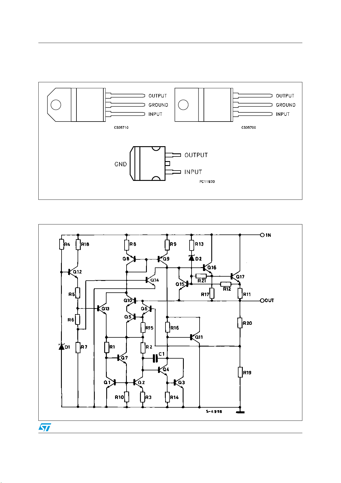
L7800AB/AC series Pin configuration
1 Pin configuration
Figure 1. Pin connections (top view)
TO-220
Figure 2. Schematic diagram
TO-220FP
D2PAK
3/28
Maximum ratings L7800AB/AC series
2 Maximum ratings
Table 1. Absolute maximum ratings
Symbol Parameter Value Unit
for V
= 5 to 18V 35
O
= 20, 24V 40
for V
O
for L7800AC 0 to 150
for L7800AB -40 to 125
V
°C
T
P
T
V
I
STG
OP
DC Input voltage
I
Output current Internally Limited mA
O
Power dissipation Internally Limited mW
D
Storage temperature range -65 to 150 °C
Operating junction temperature range
Note: Absolute Maximum Ratings are those values beyond which damage to the device may
occur. Functional operation under these condition is not implied
Table 2. Thermal Data
Symbol Parameter TO-220 TO-220FP D2PA K U ni t
R
R
thJC
thJA
Thermal resistance junction-case 3 5 3 °C/W
Thermal resistance junction-ambient 50 60 62.5 °C/W
Figure 3. Application circuits
4/28
L7800AB/AC series Test circuits
3 Test circuits
Figure 4. DC Parameter
Figure 5. Load regulation
Figure 6. Ripple rejection
5/28
Electrical characteristics L7800AB/AC series
4 Electrical characteristics
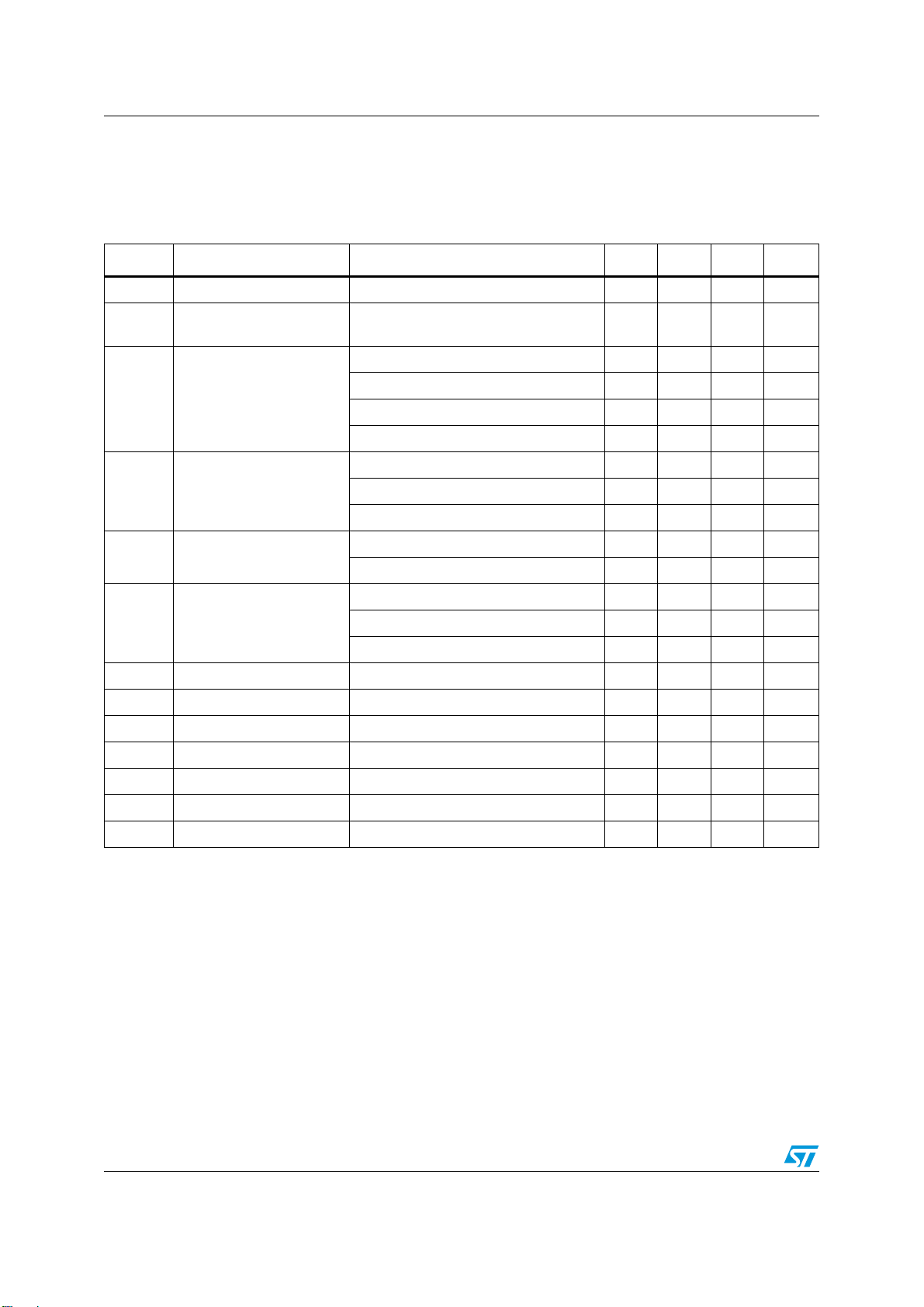
Table 3. Electrical characteristics of L7805A (VI = 10V, IO=1A, TJ = 0 to 150°C (L7805AC),
T
= -40 to 125°C (L7805AB), unless otherwise specified)
J
Symbol Parameter Test conditions Min. Typ. Max. Unit
V
V
∆V
Output voltage TJ = 25°C 4.9 5 5.1 V
O
O
(1)
O
Output voltage
Line regulation
IO = 5mA to 1A, PO ≤15W
V
= 7.5 to 20V
I
V
= 7.5 to 25V, IO = 500 mA 7 50 mV
I
V
= 8 to 12V 10 50 mV
I
4.855.2V
VI = 8 to 12V, TJ = 25°C 2 25 mV
V
= 7.3 to 20V, TJ = 25°C 7 50 mV
I
IO = 5mA to 1A 25 100 mV
∆V
(*) Load regulation
O
I
Quiescent current
q
∆I
Quiescent current change
q
IO = 5mA to 1.5A, TJ = 25°C 30 100 V
I
= 250 to 750mA 8 50 V
O
T
= 25°C 4.3 6 mA
J
6mA
= 8 to 25V, IO = 500 mA 0.8 mA
V
I
V
= 7.5 to 20V, TJ = 25°C 0.8 mA
I
IO = 5mA to 1A 0.5 mA
SVR Supply voltage rejection V
V
Dropout voltage IO = 1A, TJ = 25°C 2 V
d
= 8 to 18V, f = 120Hz, IO = 500mA 68 dB
I
eN Output noise voltage TA = 25°C, B =10Hz to 100KHz 10 µV/V
R
I
I
∆V
1. Load and line regulation are specified at constant junction temperature. Changes in VO due to heating effects must be
taken into account separately. Pulse testing with low duty cycle is used.
Output resistance f =1KHz 17 mΩ
O
Short circuit current VI = 35V, TA = 25°C 0.2 A
sc
Short circuit peak current TJ = 25°C 2.2 A
scp
/∆T Output voltage drift -1.1 mV/°C
O
O
6/28
L7800AB/AC series Electrical characteristics
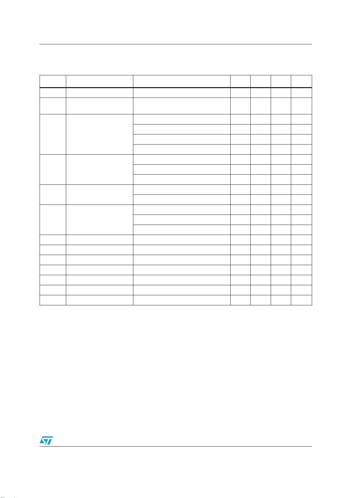
Table 4. Electrical characteristics of L7806A (VI = 11V, IO=1A, TJ = 0 to 150°C (L7806AC),
T
= -40 to 125°C (L7806AB), unless otherwise specified)
J
Symbol Parameter Test conditions Min. Typ. Max. Unit
V
V
∆V
Output voltage TJ = 25°C 5.88 6 6.12 V
O
O
(1)
O
Output voltage
Line regulation
IO = 5mA to 1A, PO ≤15W
V
= 8.6 to 21V
I
V
= 8.6 to 25V, IO = 500 mA 9 60 mV
I
V
= 9 to 13V 11 60 mV
I
5.7666.24V
VI = 9 to 13V, TJ = 25°C 3 30 mV
V
= 8.3 to 21V, TJ = 25°C 9 60 mV
I
IO = 5mA to 1A 25 100 mV
(1)
∆V
∆I
Load regulation
O
I
Quiescent current
q
Quiescent current change
q
IO = 5mA to 1.5A, TJ = 25°C 30 100 V
I
= 250 to 750mA 10 50 V
O
T
= 25°C 4.3 6 mA
J
6mA
= 9 to 25V, IO = 500 mA 0.8 mA
V
I
V
= 8.6 to 21V, TJ = 25°C 0.8 mA
I
IO = 5mA to 1A 0.5 mA
SVR Supply voltage rejection V
V
Dropout voltage IO = 1A, TJ = 25°C 2 V
d
= 9 to 19V, f = 120Hz, IO = 500mA 65 dB
I
eN Output noise voltage TA = 25°C, B =10Hz to 100KHz 10 µV/V
R
I
I
∆V
1. Load and line regulation are specified at constant junction temperature. Changes in VO due to heating effects must be
taken into account separately. Pulse testing with low duty cycle is used.
Output resistance f =1KHz 17 mΩ
O
Short circuit current VI = 35V, TA = 25°C 0.2 A
sc
Short circuit peak current TJ = 25°C 2.2 A
scp
/∆T Output voltage drift -0.8 mV/°C
O
O
7/28
Electrical characteristics L7800AB/AC series
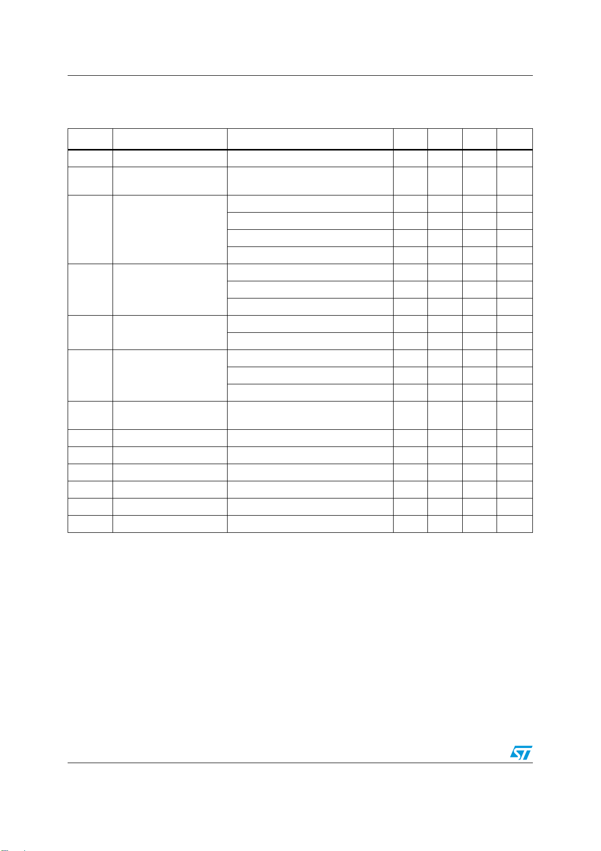
Table 5. Electrical characteristics of L7808A (VI = 14V, IO=1A, TJ = 0 to 150°C (L7808AC),
T
= -40 to 125°C (L7808AB), unless otherwise specified)
J
Symbol Parameter Test conditions Min. Typ. Max. Unit
V
V
∆V
Output voltage TJ = 25°C 7.84 8 8.16 V
O
O
(1)
O
Output voltage
Line regulation
IO = 5mA to 1A, PO ≤15W
V
= 10.6 to 23V
I
V
= 10.6 to 25V, IO = 500 mA 12 80 mV
I
V
= 11 to 17V 15 80 mV
I
7.788.3V
VI = 11 to 17V, TJ = 25°C 5 40 mV
V
= 10.4 to 23V, TJ = 25°C 12 80 mV
I
IO = 5mA to 1A 25 100 mV
(1)
∆V
∆I
Load regulation
O
I
Quiescent current
q
Quiescent current change
q
IO = 5mA to 1.5A, TJ = 25°C 30 100 V
I
= 250 to 750mA 10 50 V
O
T
= 25°C 4.3 6 mA
J
6mA
= 11 to 25V, IO = 500 mA 0.8 mA
V
I
V
= 10.6 to 23V, TJ = 25°C 0.8 mA
I
IO = 5mA to 1A 0.5 mA
= 11.5 to 21.5V, f = 120Hz,
V
SVR Supply voltage rejection
V
Dropout voltage IO = 1A, TJ = 25°C 2 V
d
eN Output noise voltage T
R
I
I
∆V
1. Load and line regulation are specified at constant junction temperature. Changes in VO due to heating effects must be
taken into account separately. Pulse testing with low duty cycle is used.
Output resistance f =1KHz 18 mΩ
O
Short circuit current VI = 35V, TA = 25°C 0.2 A
sc
Short circuit peak current TJ = 25°C 2.2 A
scp
/∆T Output voltage drift -0.8 mV/°C
O
I
= 500mA
I
O
= 25°C, B =10Hz to 100KHz 10 µV/V
A
62 dB
O
8/28
L7800AB/AC series Electrical characteristics
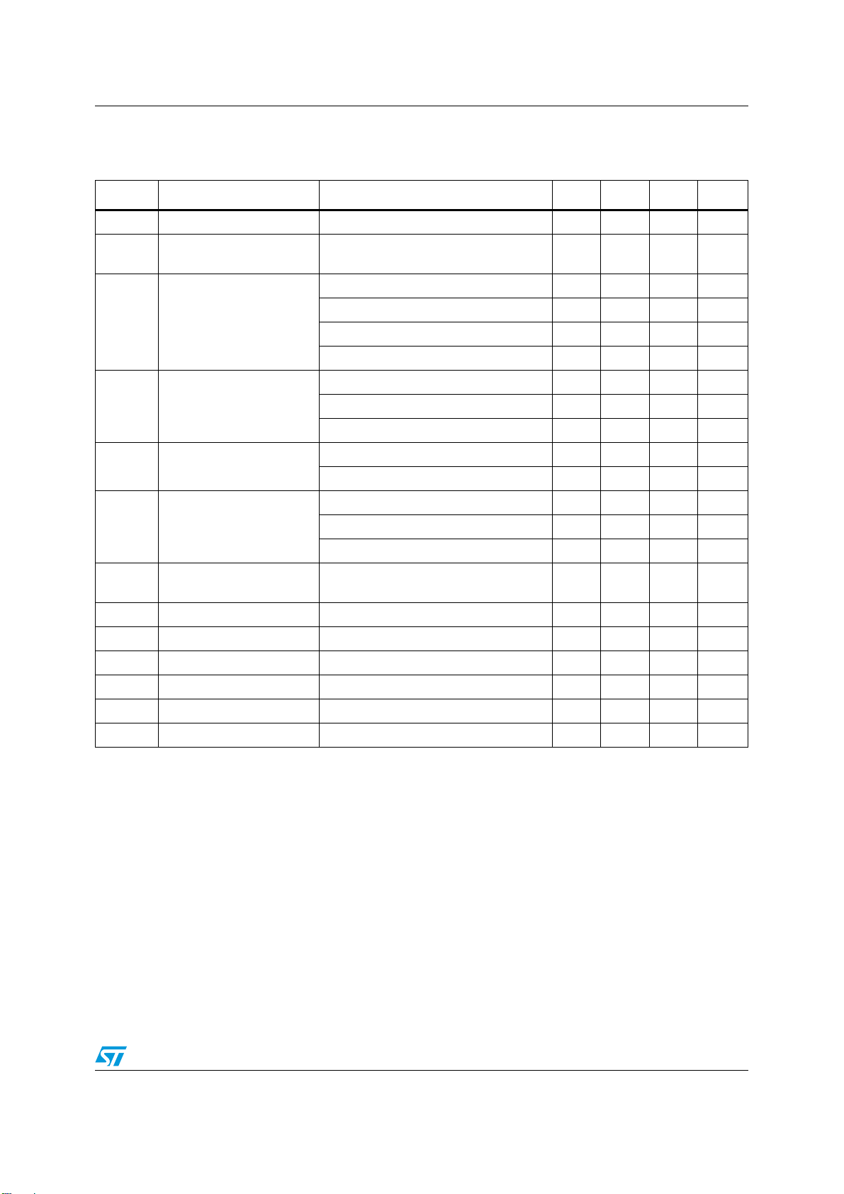
Table 6. Electrical characteristics of L7809A (VI = 15V, IO=1A, TJ = 0 to 150°C (L7809AC),
T
= -40 to 125°C (L7809AB), unless otherwise specified)
J
Symbol Parameter Test conditions Min. Typ. Max. Unit
V
V
∆V
Output voltage TJ = 25°C 8.82 9 9.18 V
O
O
(1)
O
Output voltage
Line regulation
IO = 5mA to 1A, PO ≤15W
V
= 10.6 to 23V
I
V
= 10.6 to 25V, IO = 500 mA 12 90 mV
I
V
= 11 to 17V 15 90 mV
I
8.6599.35V
VI = 11 to 17V, TJ = 25°C 5 45 mV
V
= 10.4 to 23V, TJ = 25°C 12 90 mV
I
IO = 5mA to 1A 25 100 mV
(1)
∆V
∆I
Load regulation
O
I
Quiescent current
q
Quiescent current change
q
IO = 5mA to 1.5A, TJ = 25°C 30 100 V
I
= 250 to 750mA 10 50 V
O
T
= 25°C 4.3 6 mA
J
6mA
= 11 to 25V, IO = 500 mA 0.8 mA
V
I
V
= 10.6 to 23V, TJ = 25°C 0.8 mA
I
IO = 5mA to 1A 0.5 mA
= 11.5 to 21.5V, f = 120Hz,
V
SVR Supply voltage rejection
V
Dropout voltage IO = 1A, TJ = 25°C 2 V
d
eN Output noise voltage T
R
I
I
∆V
1. Load and line regulation are specified at constant junction temperature. Changes in VO due to heating effects must be
taken into account separately. Pulse testing with low duty cycle is used.
Output resistance f =1KHz 18 mΩ
O
Short circuit current VI = 35V, TA = 25°C 0.2 A
sc
Short circuit peak current TJ = 25°C 2.2 A
scp
/∆T Output voltage drift -0.8 mV/°C
O
I
= 500mA
I
O
= 25°C, B =10Hz to 100KHz 10 µV/V
A
61 dB
O
9/28

Electrical characteristics L7800AB/AC series
Table 7. Electrical characteristics of L7812A (VI = 19V, IO=1A, TJ = 0 to 150°C (L7812AC),
T
= -40 to 125°C (L7812AB), unless otherwise specified)
J
Symbol Parameter Test conditions Min. Typ. Max. Unit
V
V
∆V
Output voltage TJ = 25°C 11.75 12 12.25 V
O
O
(1)
O
Output voltage
Line regulation
IO = 5mA to 1A, PO ≤15W
V
= 14.8 to 27V
I
V
= 14.8 to 30V, IO = 500 mA 13 120 mV
I
V
= 16 to 12V 16 120 mV
I
11.5 12 12.5 V
VI = 16 to 12V, TJ = 25°C 6 60 mV
V
= 14.5 to 27V, TJ = 25°C 13 120 mV
I
IO = 5mA to 1A 25 100 mV
(1)
∆V
∆I
Load regulation
O
I
Quiescent current
q
Quiescent current change
q
IO = 5mA to 1.5A, TJ = 25°C 30 100 V
I
= 250 to 750mA 10 50 V
O
T
= 25°C 4.4 6 mA
J
6mA
= 15 to 30V, IO = 500 mA 0.8 mA
V
I
V
= 14.8 to 27V, TJ = 25°C 0.8 mA
I
IO = 5mA to 1A 0.5 mA
SVR Supply voltage rejection V
V
Dropout voltage IO = 1A, TJ = 25°C 2 V
d
= 15 to 25V, f = 120Hz, IO = 500mA 60 dB
I
eN Output noise voltage TA = 25°C, B =10Hz to 100KHz 10 µV/V
R
I
I
∆V
1. Load and line regulation are specified at constant junction temperature. Changes in VO due to heating effects must be
taken into account separately. Pulse testing with low duty cycle is used.
Output resistance f =1KHz 18 mΩ
O
Short circuit current VI = 35V, TA = 25°C 0.2 A
sc
Short circuit peak current TJ = 25°C 2.2 A
scp
/∆T Output voltage drift -1 mV/°C
O
O
10/28

L7800AB/AC series Electrical characteristics
Table 8. Electrical characteristics of L7815A (VI = 23V, IO=1A, TJ = 0 to 150°C (L7815AC),
T
= -40 to 125°C (L7815AB), unless otherwise specified)
J
Symbol Parameter Test conditions Min. Typ. Max. Unit
V
V
∆V
Output voltage TJ = 25°C 14.7 15 15.3 V
O
O
(1)
O
Output voltage
Line regulation
IO = 5mA to 1A, PO ≤15W
V
= 17.9 to 30V
I
V
= 17.9 to 30V, IO = 500 mA 13 150 mV
I
V
= 20 to 26V 16 150 mV
I
14.4 15 15.6 V
VI = 20 to 26V, TJ = 25°C 6 75 mV
V
= 17.5 to 30V, TJ = 25°C 13 150 mV
I
IO = 5mA to 1A 25 100 mV
(1)
∆V
∆I
Load regulation
O
I
Quiescent current
q
Quiescent current change
q
IO = 5mA to 1.5A, TJ = 25°C 30 100 V
I
= 250 to 750mA 10 50 V
O
T
= 25°C 4.4 6 mA
J
6mA
= 17.5 to 30V, IO = 500 mA 0.8 mA
V
I
V
= 17.5 to 30V, TJ = 25°C 0.8 mA
I
IO = 5mA to 1A 0.5 mA
= 18.5 to 28.5V, f = 120Hz,
V
SVR Supply voltage rejection
V
Dropout voltage IO = 1A, TJ = 25°C 2 V
d
eN Output noise voltage T
R
I
I
∆V
1. Load and line regulation are specified at constant junction temperature. Changes in VO due to heating effects must be
taken into account separately. Pulse testing with low duty cycle is used.
Output resistance f =1KHz 19 mΩ
O
Short circuit current VI = 35V, TA = 25°C 0.2 A
sc
Short circuit peak current TJ = 25°C 2.2 A
scp
/∆T Output voltage drift -1 mV/°C
O
I
= 500mA
I
O
= 25°C, B =10Hz to 100KHz 10 µV/V
A
58 dB
O
11/28

Electrical characteristics L7800AB/AC series
Table 9. Electrical characteristics of L7818A (VI = 27V, IO=1A, TJ = 0 to 150°C (L7818AC),
T
= -40 to 125°C (L7818AB), unless otherwise specified)
J
Symbol Parameter Test conditions Min. Typ. Max. Unit
V
V
∆V
Output voltage TJ = 25°C 17.64 18 18.36 V
O
O
(1)
O
Output voltage
Line regulation
IO = 5mA to 1A, PO ≤15W
V
= 21 to 33V
I
V
= 21 to 33V, IO = 500 mA 25 180 mV
I
V
= 24 to 30V 28 180 mV
I
17.3 18 18.7 V
VI = 24 to 30V, TJ = 25°C 10 90 mV
V
= 20.6 to 33V, TJ = 25°C 5 180 mV
I
IO = 5mA to 1A 25 100 mV
(1)
∆V
∆I
Load regulation
O
I
Quiescent current
q
Quiescent current change
q
IO = 5mA to 1.5A, TJ = 25°C 30 100 V
I
= 250 to 750mA 10 50 V
O
T
= 25°C 4.5 6 mA
J
6mA
= 21 to 33V, IO = 500 mA 0.8 mA
V
I
V
= 21 to 33V, TJ = 25°C 0.8 mA
I
IO = 5mA to 1A 0.5 mA
SVR Supply voltage rejection V
V
Dropout voltage IO = 1A, TJ = 25°C 2 V
d
= 22 to 32V, f = 120Hz, IO = 500mA 57 dB
I
eN Output noise voltage TA = 25°C, B =10Hz to 100KHz 10 µV/V
R
I
I
∆V
1. Load and line regulation are specified at constant junction temperature. Changes in VO due to heating effects must be
taken into account separately. Pulse testing with low duty cycle is used.
Output resistance f =1KHz 19 mΩ
O
Short circuit current VI = 35V, TA = 25°C 0.2 A
sc
Short circuit peak current TJ = 25°C 2.2 A
scp
/∆T Output voltage drift -1 mV/°C
O
O
12/28

L7800AB/AC series Electrical characteristics
Table 10. Electrical characteristics of L7820A (VI = 28V, IO=1A, TJ = 0 to 150°C (L7820AC),
T
= -40 to 125°C (L7820AB), unless otherwise specified)
J
Symbol Parameter Test conditions Min. Typ. Max. Unit
V
V
∆V
Output voltage TJ = 25°C 19.6 20 20.4 V
O
O
(1)
O
Output voltage
Line regulation
IO = 5mA to 1A, PO ≤15W
V
= 23 to 35V
I
V
= 23 to 35V, IO = 500 mA 200 mV
I
V
= 26 to 32V 200 mV
I
19.2 20 20.8 V
VI = 26 to 32V, TJ = 25°C 100 mV
V
= 23 to 32V, TJ = 25°C 200 mV
I
IO = 5mA to 1A 25 100 mV
(1)
∆V
∆I
Load regulation
O
I
Quiescent current
q
Quiescent current change
q
IO = 5mA to 1.5A, TJ = 25°C 30 100 V
I
= 250 to 750mA 10 50 V
O
T
= 25°C 4.5 6 mA
J
6mA
= 23 to 35V, IO = 500 mA 0.8 mA
V
I
V
= 23 to 35V, TJ = 25°C 0.8 mA
I
IO = 5mA to 1A 0.5 mA
SVR Supply voltage rejection V
V
Dropout voltage IO = 1A, TJ = 25°C 2 V
d
= 24 to 35V, f = 120Hz, IO = 500mA 56 dB
I
eN Output noise voltage TA = 25°C, B =10Hz to 100KHz 10 µV/V
R
I
I
∆V
1. Load and line regulation are specified at constant junction temperature. Changes in VO due to heating effects must be
taken into account separately. Pulse testing with low duty cycle is used.
Output resistance f =1KHz 20 mΩ
O
Short circuit current VI = 35V, TA = 25°C 0.2 A
sc
Short circuit peak current TJ = 25°C 2.2 A
scp
/∆T Output voltage drift -1 mV/°C
O
O
13/28

Electrical characteristics L7800AB/AC series
Table 11. Electrical characteristics of L7824A (VI = 33V, IO=1A, TJ = 0 to 150°C (L7824AC),
T
= -40 to 125°C (L7824AB), unless otherwise specified)
J
Symbol Parameter Test conditions Min. Typ. Max. Unit
V
V
∆V
Output voltage TJ = 25°C 19.6 20 20.4 V
O
O
(1)
O
Output voltage
Line regulation
IO = 5mA to 1A, PO ≤15W
V
= 27.3 to 38V
I
V
= 27 to 38V, IO = 500 mA 200 mV
I
V
= 30 to 36V 200 mV
I
19.2 20 20.8 V
VI = 30 to 36V, TJ = 25°C 100 mV
V
= 26.7 to 38V, TJ = 25°C 200 mV
I
IO = 5mA to 1A 25 100 mV
(1)
∆V
∆I
Load regulation
O
I
Quiescent current
q
Quiescent current change
q
IO = 5mA to 1.5A, TJ = 25°C 30 100 V
I
= 250 to 750mA 10 50 V
O
T
= 25°C 4.5 6 mA
J
6mA
= 27.3 to 38V, IO = 500 mA 0.8 mA
V
I
V
= 27.3 to 38V, TJ = 25°C 0.8 mA
I
IO = 5mA to 1A 0.5 mA
SVR Supply voltage rejection V
V
Dropout voltage IO = 1A, TJ = 25°C 2 V
d
= 28 to 38V, f = 120Hz, IO = 500mA 56 dB
I
eN Output noise voltage TA = 25°C, B =10Hz to 100KHz 10 µV/V
R
I
I
∆V
1. Load and line regulation are specified at constant junction temperature. Changes in VO due to heating effects must be
taken into account separately. Pulse testing with low duty cycle is used.
Output resistance f =1KHz 20 mΩ
O
Short circuit current VI = 35V, TA = 25°C 0.2 A
sc
Short circuit peak current TJ = 25°C 2.2 A
scp
/∆T Output voltage drift -1 mV/°C
O
O
14/28

L7800AB/AC series Application information
5 Application information
5.1 Design consideration
The L7800A Series of fixed voltage regulators are designed with Thermal Overload
Protection that shuts down the circuit when subjected to an excessive power overload
condition, Internal Short-circuit Protection that limits the maximum current the circuit will
pass, and Output transistor Safe-Area Compensation that reduces the output short-circuit
current as the voltage across the pass transistor is increased. In many low current
applications, compensation capacitors are not required. However, it is recommended that
the regulator input be bypassed with capacitor if the regulator is connected to the power
supply filter with long lengths, or if the output load capacitance is large. An input bypass
capacitor should be selected to provide good high frequency characteristics to insure stable
operation under all load conditions. A 0.33µF or larger tantalum, mylar or other capacitor
having low internal impedance at high frequencies should be chosen. The bypass capacitor
should be mounted with the shortest possible leads directly across the regulators input
terminals. Normally good construction techniques should be used to minimize ground loops
and lead resistance drops since the regulator has no external sense lead.
The addition of an operational amplifier allows adjustment to higher or intermediate values
while retaining regulation characteristics. The minimum voltage obtained with the
arrangement is 2V greater than the regulator voltage.
The circuit of figure 6 can be modified to provide supply protection against short circuit by
adding a short circuit sense resistor, RSC, and an additional PNP transistor. The current
sensing PNP must be able to handle the short circuit current of the three terminal regulator
Therefore a four ampere plastic power transistor is specified.
Figure 7. DC Parameter
IO = VXX/R1+I
d
15/28

Application information L7800AB/AC series
Figure 8. DC Parameter
VO = 7 to 20V
VI - VO ≥ 2V
Figure 9. DC Parameter
V
I
REQ
REG
BEQ1
-(IQ1/βQ1)
+ Q1 (I
REG
______)
R1 = ______________
IO = I
.
V
BEQ1
R
1
16/28

L7800AB/AC series Application information
Figure 10. DC Parameter
17/28

Package mechanical data L7800AB/AC series
6 Package mechanical data
In order to meet environmental requirements, ST offers these devices in ECOPACK®
packages. These packages have a Lead-free second level interconnect. The category of
second Level Interconnect is marked on the package and on the inner box label, in
compliance with JEDEC Standard JESD97. The maximum ratings related to soldering
conditions are also marked on the inner box label. ECOPACK is an ST trademark.
ECOPACK specifications are available at: www.st.com.
18/28

L7800AB/AC series Package mechanical data
TO-220 MECHANICAL DAT
DIM.
A 4.40 4.60 0.173 0.181
C 1.23 1.32 0.048 0.051
D 2.40 2.72 0.094 0.107
D1 1.27 0.050
E 0.49 0.70 0.019 0.027
F 0.61 0.88 0.024 0.034
F1 1.14 1.70 0.044 0.067
F2 1.14 1.70 0.044 0.067
G 4.95 5.15 0.194 0.203
G1 2.4 2.7 0.094 0.106
H2 10.0 10.40 0.393 0.409
L2 16.4 0.645
L4 13.0 14.0 0.511 0.551
L5 2.65 2.95 0.104 0.116
L6 15.25 15.75 0.600 0.620
L7 6.2 6.6 0.244 0.260
L9 3.5 3.93 0.137 0.154
DIA. 3.75 3.85 0.147 0.151
MIN. TYP MAX. MIN. TYP. MAX.
mm. inch
A
P011C
19/28

Package mechanical data L7800AB/AC series
TO-220FP MECHANICAL DATA
DIM.
A 4.40 4.60 0.173 0.181
B 2.5 2.7 0.098 0.106
D 2.5 2.75 0.098 0.108
E 0.45 0.70 0.017 0.027
F 0.75 1 0.030 0.039
F1 1.15 1.50 0.045 0.059
F2 1.15 1.50 0.045 0.059
G 4.95 5.2 0.194 0.204
G1 2.4 2.7 0.094 0.106
H 10.0 10.40 0.393 0.409
L2 16 0.630
L3 28.6 30.6 1.126 1.204
L4 9.8 10.6 0.385 0.417
L5 2.9 3.6 0.114 0.142
L6 15.9 16.4 0.626 0.645
L7 9 9.3 0.354 0.366
DIA. 3 3.2 0.118 0.126
MIN. TYP MAX. MIN. TYP. MAX.
mm. inch
20/28
7012510A-H

L7800AB/AC series Package mechanical data
Figure 11. DRAWING DIMENSION D2PAK (TYPE STD-ST)
0079457/L
21/28

Package mechanical data L7800AB/AC series
Figure 12. DRAWING DIMENSION D2PAK (TYPE WOOSEOK-SUBCON.)
22/28
0079457/L

L7800AB/AC series Package mechanical data
Table 12. D2PAK MECHANICAL DATA
TYPE STD-ST TYPE WOOSEOK-SUBCON.
DIM.
MIN. TYP. MAX. MIN. TYP. MAX.
A 4.40 4.60 4.30 4.70
A1 0.03 0.23 0 0.20
b 0.70 0.93 0.70 0.90
b2 1.14 1.70 1.17 1.37
c 0.45 0.60 0.45 0.50 0.60
c2 1.23 1.36 1.25 1.30 1.40
D 8.95 9.35 9 9.20 9.40
D1 7.50 7.50
E 10 10.40 9.80 10.20
E1 8.50 7.50
e2.54 2.54
e1 4.88 5.28 5.08
H 15 15.85 15 15.30 15.60
J1 2.49 2.69 2.20 2.60
L 2.29 2.79 1.79 2.79
L1 1.27 1.40 1 1.40
mm. mm.
L2 1.30 1.75 1.20 1.60
R0.4 0.30
V2 0° 8° 0° 3°
Note: The D2PAK package coming from the subcontractor Wooseok is fully compatible with the
ST's package suggested footprint.
23/28

Package mechanical data L7800AB/AC series
Figure 13. D2PAK FOOTPRINT RECOMMENDED DATA
Table 13. FOOTPRINT DATA
A 12.20 0.480
B 9.75 0.384
C 16.90 0.665
D 3.50 0.138
E 1.60 0.063
F 2.54 0.100
G 5.08 0.200
VALUES
mm. inch.
24/28

L7800AB/AC series Package mechanical data
Tape & Reel D
DIM.
A 180 7.086
C 12.8 13.0 13.2 0.504 0.512 0.519
D 20.2 0.795
N 60 2.362
T 14.4 0.567
Ao 10.50 10.6 10.70 0.413 0.417 0.421
Bo 15.70 15.80 15.90 0.618 0.622 0.626
Ko 4.80 4.90 5.00 0.189 0.193 0.197
Po 3.9 4.0 4.1 0.153 0.157 0.161
P 11.9 12.0 12.1 0.468 0.472 0.476
2
PAK-P2PAK-D2PAK/A-P2PAK/A MECHANICAL DATA
mm. inch
MIN. TYP MAX. MIN. TYP. MAX.
25/28

Order code L7800AB/AC series
7 Order code
Table 14. Order code
Packaging
Part numbers
TO-220 TO-220FP D
2
PAK
L7805AB L7805ABV L7805ABP L7805ABD2T-TR 5 V
L7805AC L7805ACV L7805ACP L7805ACD2T-TR 5 V
L7806AB L7806ABV L7806ABP
L7806AC L7806ACV L7806ACP
(1)
(1)
L7806ABD2T-TR 6 V
L7806ACD2T-TR 6 V
L7808AB L7808ABV L7808ABP L7808ABD2T-TR 8 V
L7808AC L7808ACV L7808ACP L7808ACD2T-TR 8 V
L7809AB L7809ABV L7809ABP L7809ABD2T-TR 9 V
L7809AC L7809ACV L7809ACP L7809ACD2T-TR 9 V
L7812AB L7812ABV L7812ABP
(1)
L7812ABD2T-TR 12 V
L7812AC L7812ACV L7812ACP L7812ACD2T-TR 12 V
Output voltage
L7815AB L7815ABV L7815ABP L7815ABD2T-TR 15 V
L7815AC L7815ACV L7815ACP
L7818AB L7818ABV L7818ABP L7818ABD2T-TR
L7818AC L7818ACV L7818ACP
L7820AB L7820ABV
(1)
L7820ABP
L7820AC L7820ACV L7820ACP
L7824AB L7824ABV L7824ABP L7824ABD2T-TR
L7824AC L7824ACV L7824ACP
1. Available on request.
(1)
(1)
(1)
(1)
(1)
L7815ACD2T-TR 15 V
(1)
L7818ACD2T-TR
L7820ABD2T-TR
L7820ACD2T-TR
L7824ACD2T-TR
(1)
(1)
(1)
(1)
(1)
18 V
18 V
20 V
20 V
24 V
24 V
26/28

L7800AB/AC series Revision history
8 Revision history
Table 15. Revision history
Date Revision Changes
21-Jun-2004 9 Document updating.
04-Aug-2006 10 Order Codes has been updated and new template.
19-Jan-2007 11 D
2
PAK mechanical data has been updated and add footprint data.
27/28

L7800AB/AC series
Please Read Carefully:
Information in this document is provided solely in connection with ST products. STMicroelectronics NV and its subsidiaries (“ST”) reserve the
right to make changes, corrections, modifications or improvements, to this document, and the products and services described herein at any
time, without notice.
All ST products are sold pursuant to ST’s terms and conditions of sale.
Purchasers are solely responsible for the choice, selection and use of the ST products and services described herein, and ST assumes no
liability whatsoever relating to the choice, selection or use of the ST products and services described herein.
No license, express or implied, by estoppel or otherwise, to any intellectual property rights is granted under this document. If any part of this
document refers to any third party products or services it shall not be deemed a license grant by ST for the use of such third party products
or services, or any intellectual property contained therein or considered as a warranty covering the use in any manner whatsoever of such
third party products or services or any intellectual property contained therein.
UNLESS OTHERWISE SET FORTH IN ST’S TERMS AND CONDITIONS OF SALE ST DISCLAIMS ANY EXPRESS OR IMPLIED
WARRANTY WITH RESPECT TO THE USE AND/OR SALE OF ST PRODUCTS INCLUDING WITHOUT LIMITATION IMPLIED
WARRANTIES OF MERCHANTABILITY, FITNESS FOR A PARTICULAR PURPOSE (AND THEIR EQUIVALENTS UNDER THE LAWS
OF ANY JURISDICTION), OR INFRINGEMENT OF ANY PATENT, COPYRIGHT OR OTHER INTELLECTUAL PROPERTY RIGHT.
UNLESS EXPRESSLY APPROVED IN WRITING BY AN AUTHORIZED ST REPRESENTATIVE, ST PRODUCTS ARE NOT
RECOMMENDED, AUTHORIZED OR WARRANTED FOR USE IN MILITARY, AIR CRAFT, SPACE, LIFE SAVING, OR LIFE SUSTAINING
APPLICATIONS, NOR IN PRODUCTS OR SYSTEMS WHERE FAILURE OR MALFUNCTION MAY RESULT IN PERSONAL INJURY,
DEATH, OR SEVERE PROPERTY OR ENVIRONMENTAL DAMAGE. ST PRODUCTS WHICH ARE NOT SPECIFIED AS "AUTOMOTIVE
GRADE" MAY ONLY BE USED IN AUTOMOTIVE APPLICATIONS AT USER’S OWN RISK.
Resale of ST products with provisions different from the statements and/or technical features set forth in this document shall immediately void
any warranty granted by ST for the ST product or service described herein and shall not create or extend in any manner whatsoever, any
liability of ST.
ST and the ST logo are trademarks or registered trademarks of ST in various countries.
Information in this document supersedes and replaces all information previously supplied.
The ST logo is a registered trademark of STMicroelectronics. All other names are the property of their respective owners.
© 2007 STMicroelectronics - All rights reserved
STMicroelectronics group of companies
Australia - Belgium - Brazil - Canada - China - Czech Republic - Finland - France - Germany - Hong Kong - India - Israel - Italy - Japan -
Malaysia - Malta - Morocco - Singapore - Spain - Sweden - Switzerland - United Kingdom - United States of America
www.st.com
28/28
 Loading...