

现货库存、技术资料、百科信息、热点资讯,精彩尽在鼎好!
POSITIVE VOLTAGE REGULATORS
L7800
SERIES
■ OUTPUT CURRENT TO 1.5A
■ OUTPUT VOLTAGES OF 5; 5.2; 6; 8; 8.5; 9;
10; 12; 15; 18; 24V
■ THERMAL OVERLOAD PROTECTION
■ SHORT CIRCUIT PROTECTION
■ OUTPUT TRANSITION SOA PROTECTION
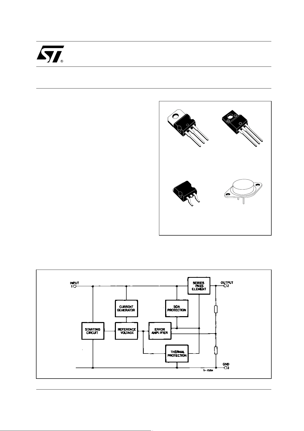
DESCRIPTION
The L7800 series of three-terminal positive
regulators is available in TO-220, TO-220FP,
TO-220FM, TO-3 and D
2
PAK packages and
several fixed output voltages, making it useful in a
wide range of applications. These regulators c an
provide local on-card regulation, eliminating the
distribution problems associated w ith single point
regulation. Each type employs internal current
limiting, thermal shut-down and safe area
protection, making it essentially indestructible. If
adequate heat sinking is provided, they can
deliver over 1A output current. Although designed
primarily as fixed voltage regulators, these
devices can be us ed with ex ternal components to
obtain adjustable voltage and currents.
TO-220
D2PAK TO-3
TO-220FP
TO-220FM
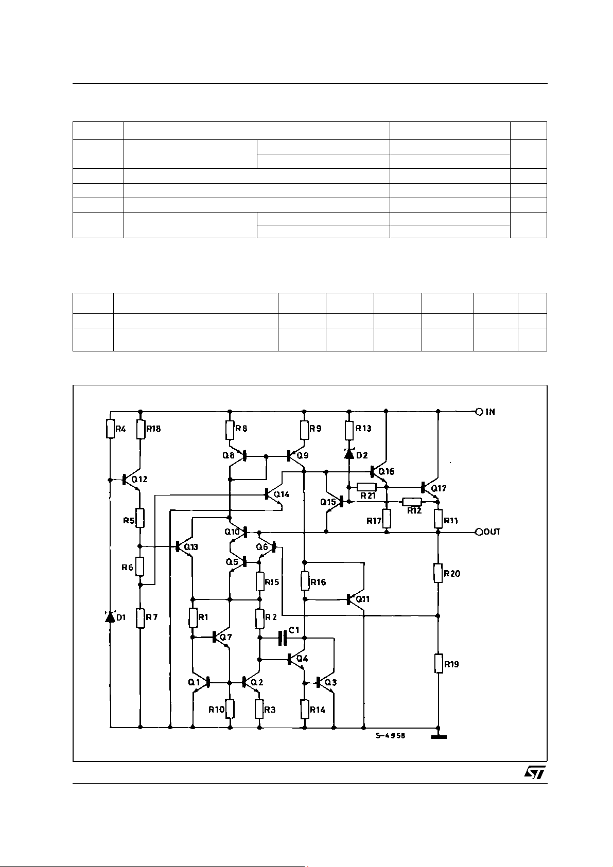
Figure 1: Schematic Diagram
Rev. 12
1/34November 2004
L7800 SERIES
Table 1: Absolute Maximum Ratings
Symbol Parameter Value Unit
V
I
P
T
T
Absolute Maximum Ratings are those values beyond which damage to the device may occur. Functional operation under these condition is
not implied.
DC Input Voltage for VO= 5 to 18V
I
Output Current
O
Power Dissipation
tot
Storage Temperature Range
stg
Operating Junction T emperature
op
Range
for V
= 20, 24V
O
for L7800 -55 to 150
for L7800C 0 to 150
Table 2: Thermal Data
35
40
Internally Limited
Internally Limited
-65 to 150 °C
V
°C
Symbol Parameter
R
thj-case
R
thj-amb
Thermal Resistance Junction-case Max
Thermal Resistance Junction-ambient
Max
Figure 2: Schematic Diagram
2
PAK
D
TO-220 TO-220FP TO-220FM TO-3 Unit
355 54°C/W
62.5 50 60 60 35 °C/W
2/34
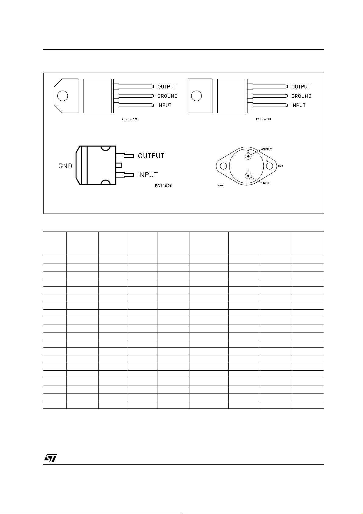
Figure 3: Connection Di agram (top view)
L7800 SERIES
TO-220 (Any Type)
2
PAK (Any Ty p e )
TO-220FP/TO-220FM
TO-3D
Table 3: Order Codes
2
PAK
TYPE
L7805 L7805T
L7805C L7805CV L7805C-V L7805CV1 L7805CD2T L7805C-D2TR L7805CP L7805CF L7805CT
L7852C L7852CV L7852CD2T L7852CP L7852CF L7852CT
L7806 L7806T
L7806C L7806CV L7806C-V L7806CD2T L7806CP L7806CF L7806CT
L7808 L7808T
L7808C L7808CV L7808C-V L7808CD2T L7808CP L7808CF L7808CT
L7885C L7885CV L7885CD2T L7885CP L7885CF L7885CT
L7809C L7809CV L7809C-V L7809CD2T L7809CP L7809CF L7809CT
L7810C L7810CV L7810CD2T L7810CP
L7812 L7812T
L7812C L7812CV L7812C-V L7812CD2T L7812CP L7812CF L7812CT
L7815 L7815T
L7815C L7815CV L7815C-V L7815CD2T L7815CP L7815CF L7815CT
L7818 L7818T
L7818C L7818CV L7818CD2T L7818CP L7818CF L7818CT
L7820 L7820T
L7820C L7820CV L7820CD2T L7820CP L7820CF L7820CT
L7824 L7824T
L7824C L7824CV L7824CD2T L7824CP L7824CF L7824CT
(*) Avai l abl e in Tape & Re el wi th the suffix "-TR".
TO-220
(A Type)
TO-220
(C Type)
TO-220
(E Type)
2
D
PAK
(A Type) (*)
D
(C Type)
(T & R)
TO-220FP TO-220FM TO-3
3/34
L7800 SERIES
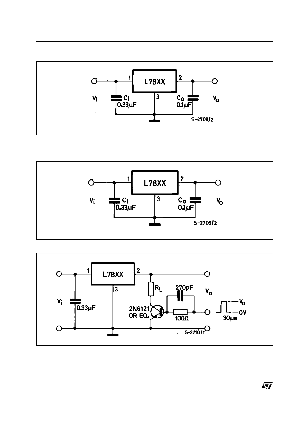
Figure 4: Appl i cation Ci rcuits
TEST CIRCUITS
Figure 5: DC Parameter
Figure 6: Load Re gulation
4/34
Figure 7: Ripp l e Rejection
L7800 SERIES
Table 4: Electrical Characteristics Of L7805 (refer to the test c ircuits, T
= 500 mA, CI = 0.33 µF, CO = 0.1 µF unless otherwise specified).
I
O
= -55 to 150°C, VI = 10V,
J
Symbol Parameter Test Conditions Min. Typ. Max. Unit
V
Output Voltage TJ = 25°C 4.8 5 5.2 V
O
Output Voltage IO = 5 mA to 1 A PO ≤ 15W
V
O
(*) Line Regulation VI = 7 to 25 V TJ = 25°C 3 50 mV
∆V
O
(*) Load Regulation IO = 5 mA to 1.5 A TJ = 25°C 100 mV
∆V
O
Quiescent Current TJ = 25°C 6 mA
I
d
∆I
Quiescent Current Change IO = 5 mA to 1 A 0.5 mA
d
/∆T Output Voltage Drift IO = 5 mA 0.6 mV/°C
∆V
O
eN Output Noise Voltage B =10Hz to 100KHz T
V
= 8 to 20 V
I
V
= 8 to 12 V TJ = 25°C 1 25
I
= 250 to 750 mA TJ = 25°C 25
I
O
= 8 to 25 V 0.8
V
I
= 25°C 40 µV/V
J
4.65 5 5.35 V
O
SVR Supply Voltage Rejection VI = 8 to 18 V f = 120Hz 68 dB
V
Dropout Voltage IO = 1 A TJ = 25°C 2 2.5 V
d
Output Resistance f = 1 KHz 17 mΩ
R
O
Short Circuit Current VI = 35 V TJ = 25°C 0.75 1.2 A
I
sc
Short Circuit Peak Current TJ = 25°C 1.3 2.2 3.3 A
I
scp
(*) Load and line regulation are specified at constant junction temperature. Changes in VO due to heating effects must be taken into account
separately. Pulse testing with low duty cycle is used.
5/34
L7800 SERIES
Table 5: Electrical Characteristics Of L7806 (refer to the test c ircuits, TJ = -55 to 150°C, VI = 11V,
= 500 mA, CI = 0.33 µF, CO = 0.1 µF unless otherwise specified).
I
O
Symbol Parameter Test Conditions Min. Typ. Max. Unit
V
Output Voltage TJ = 25°C 5.75 6 6.25 V
O
V
Output Voltage IO = 5 mA to 1 A PO ≤ 15W
O
(*) Line Regulation VI = 8 to 25 V TJ = 25°C 60 mV
∆V
O
(*) Load Regulation IO = 5 mA to 1.5 A TJ = 25°C 100 mV
∆V
O
Quiescent Current TJ = 25°C 6 mA
I
d
Quiescent Current Change IO = 5 mA to 1 A 0.5 mA
∆I
d
/∆T Output Voltage Drift IO = 5 mA 0.7 mV/°C
∆V
O
eN Output Noise Voltage B =10Hz to 100KHz T
V
= 9 to 21 V
I
= 9 to 13 V TJ = 25°C 30
V
I
I
= 250 to 750 mA TJ = 25°C 30
O
= 9 to 25 V 0.8
V
I
= 25°C 40 µV/V
J
SVR Supply Voltage Rejection VI = 9 to 19 V f = 120Hz 65 dB
Dropout Voltage IO = 1 A TJ = 25°C 2 2.5 V
V
d
Output Resistance f = 1 KHz 19 mΩ
R
O
I
Short Circuit Current VI = 35 V TJ = 25°C 0.75 1.2 A
sc
Short Circuit Peak Current TJ = 25°C 1.3 2.2 3.3 A
I
scp
(*) Load and line regulation are specified at constant junction temperature. Changes in VO due to heating effects must be taken into account
separately. Pulse testing with low duty cycle is used.
5.65 6 6.35 V
O
Table 6: Electrical Characteristics Of L7808 (refer to the test c ircuits, TJ = -55 to 150°C, VI = 14V,
= 500 mA, CI = 0.33 µF, CO = 0.1 µF unless otherwise specified).
I
O
Symbol Parameter Test Conditions Min. Typ. Max. Unit
Output Voltage TJ = 25°C 7.7 8 8.3 V
V
O
Output Voltage IO = 5 mA to 1 A PO ≤ 15W
V
O
(*) Line Regulation VI = 10.5 to 25 V TJ = 25°C 80 mV
∆V
O
(*) Load Regulation IO = 5 mA to 1.5 A TJ = 25°C 100 mV
∆V
O
Quiescent Current TJ = 25°C 6 mA
I
d
∆I
Quiescent Current Change IO = 5 mA to 1 A 0.5 mA
d
/∆T Output Voltage Drift IO = 5 mA 1 mV/°C
∆V
O
eN Output Noise Voltage B =10Hz to 100KHz T
V
= 11.5 to 23 V
I
= 11 to 17 V TJ = 25°C 40
V
I
I
= 250 to 750 mA TJ = 25°C 40
O
= 11.5 to 25 V 0.8
V
I
= 25°C 40 µV/V
J
SVR Supply Voltage Rejection VI = 11.5 to 21.5 V f = 120Hz 62 dB
V
Dropout Voltage IO = 1 A TJ = 25°C 2 2.5 V
d
Output Resistance f = 1 KHz 16 mΩ
R
O
Short Circuit Current VI = 35 V TJ = 25°C 0.75 1.2 A
I
sc
Short Circuit Peak Current TJ = 25°C 1.3 2.2 3.3 A
I
scp
(*) Load and line regulation are specified at constant junction temperature. Changes in VO due to heating effects must be taken into account
separately. Pulse testing with low duty cycle is used.
7.688.4V
O
6/34

L7800 SERIES
Table 7: Electrical Characteristics Of L7812 (refer to the test c ircuits, TJ = -55 to 150°C, VI = 19V,
= 500 mA, CI = 0.33 µF, CO = 0.1 µF unless otherwise specified).
I
O
Symbol Parameter Test Conditions Min. Typ. Max. Unit
V
Output Voltage TJ = 25°C 11.5 12 12.5 V
O
V
Output Voltage IO = 5 mA to 1 A PO ≤ 15W
O
(*) Line Regulation VI = 14.5 to 30 V TJ = 25°C 120 mV
∆V
O
(*) Load Regulation IO = 5 mA to 1.5 A TJ = 25°C 100 mV
∆V
O
Quiescent Current TJ = 25°C 6 mA
I
d
Quiescent Current Change IO = 5 mA to 1 A 0.5 mA
∆I
d
/∆T Output Voltage Drift IO = 5 mA 1.5 mV/°C
∆V
O
eN Output Noise Voltage B =10Hz to 100KHz T
V
= 15.5 to 27 V
I
= 16 to 22 V TJ = 25°C 60
V
I
I
= 250 to 750 mA TJ = 25°C 60
O
= 15 to 30 V 0.8
V
I
= 25°C 40 µV/V
J
SVR Supply Voltage Rejection VI = 15 to 25 V f = 120Hz 61 dB
Dropout Voltage IO = 1 A TJ = 25°C 2 2.5 V
V
d
Output Resistance f = 1 KHz 18 mΩ
R
O
I
Short Circuit Current VI = 35 V TJ = 25°C 0.75 1.2 A
sc
Short Circuit Peak Current TJ = 25°C 1.3 2.2 3.3 A
I
scp
(*) Load and line regulation are specified at constant junction temperature. Changes in VO due to heating effects must be taken into account
separately. Pulse testing with low duty cycle is used.
11.4 12 12.6 V
O
Table 8: Electrical Characteristics Of L7815 (refer to the test c ircuits, TJ = -55 to 150°C, VI = 23V,
= 500 mA, CI = 0.33 µF, CO = 0.1 µF unless otherwise specified).
I
O
Symbol Parameter Test Conditions Min. Typ. Max. Unit
Output Voltage TJ = 25°C 14.4 15 15.6 V
V
O
Output Voltage IO = 5 mA to 1 A PO ≤ 15W
V
O
(*) Line Regulation VI = 17.5 to 30 V TJ = 25°C 150 mV
∆V
O
(*) Load Regulation IO = 5 mA to 1.5 A TJ = 25°C 150 mV
∆V
O
Quiescent Current TJ = 25°C 6 mA
I
d
∆I
Quiescent Current Change IO = 5 mA to 1 A 0.5 mA
d
/∆T Output Voltage Drift IO = 5 mA 1.8 mV/°C
∆V
O
eN Output Noise Voltage B =10Hz to 100KHz T
V
= 18.5 to 30 V
I
= 20 to 26 V TJ = 25°C 75
V
I
I
= 250 to 750 mA TJ = 25°C 75
O
= 18.5 to 30 V 0.8
V
I
= 25°C 40 µV/V
J
SVR Supply Voltage Rejection VI = 18.5 to 28.5 V f = 120Hz 60 dB
V
Dropout Voltage IO = 1 A TJ = 25°C 2 2.5 V
d
Output Resistance f = 1 KHz 19 mΩ
R
O
Short Circuit Current VI = 35 V TJ = 25°C 0.75 1.2 A
I
sc
Short Circuit Peak Current TJ = 25°C 1.3 2.2 3.3 A
I
scp
(*) Load and line regulation are specified at constant junction temperature. Changes in VO due to heating effects must be taken into account
separately. Pulse testing with low duty cycle is used.
14.25 15 15.75 V
O
7/34

L7800 SERIES
Table 9: Electrical Characteristics Of L7818 (refer to the test c ircuits, TJ = -55 to 150°C, VI = 26V,
= 500 mA, CI = 0.33 µF, CO = 0.1 µF unless otherwise specified).
I
O
Symbol Parameter Test Conditions Min. Typ. Max. Unit
V
Output Voltage TJ = 25°C 17.3 18 18.7 V
O
V
Output Voltage IO = 5 mA to 1 A PO ≤ 15W
O
(*) Line Regulation VI = 21 to 33 V TJ = 25°C 180 mV
∆V
O
(*) Load Regulation IO = 5 mA to 1.5 A TJ = 25°C 180 mV
∆V
O
Quiescent Current TJ = 25°C 6 mA
I
d
Quiescent Current Change IO = 5 mA to 1 A 0.5 mA
∆I
d
/∆T Output Voltage Drift IO = 5 mA 2.3 mV/°C
∆V
O
eN Output Noise Voltage B =10Hz to 100KHz T
V
= 22 to 33 V
I
= 24 to 30 V TJ = 25°C 90
V
I
I
= 250 to 750 mA TJ = 25°C 90
O
= 22 to 33 V 0.8
V
I
= 25°C 40 µV/V
J
SVR Supply Voltage Rejection VI = 22 to 32 V f = 120Hz 59 dB
Dropout Voltage IO = 1 A TJ = 25°C 2 2.5 V
V
d
Output Resistance f = 1 KHz 22 mΩ
R
O
I
Short Circuit Current VI = 35 V TJ = 25°C 0.75 1.2 A
sc
Short Circuit Peak Current TJ = 25°C 1.3 2.2 3.3 A
I
scp
(*) Load and line regulation are specified at constant junction temperature. Changes in VO due to heating effects must be taken into account
separately. Pulse testing with low duty cycle is used.
17.1 18 18.9 V
O
Table 10: Electrical Characteristics Of L7820 (refer to the test circuits, TJ = -55 to 150°C, VI = 28V,
= 500 mA, CI = 0.33 µF, CO = 0.1 µF unless otherwise specified).
I
O
Symbol Parameter Test Conditions Min. Typ. Max. Unit
Output Voltage TJ = 25°C 19.2 20 20.8 V
V
O
Output Voltage IO = 5 mA to 1 A PO ≤ 15W
V
O
(*) Line Regulation VI = 22.5 to 35 V TJ = 25°C 200 mV
∆V
O
(*) Load Regulation IO = 5 mA to 1.5 A TJ = 25°C 200 mV
∆V
O
Quiescent Current TJ = 25°C 6 mA
I
d
∆I
Quiescent Current Change IO = 5 mA to 1 A 0.5 mA
d
/∆T Output Voltage Drift IO = 5 mA 2.5 mV/°C
∆V
O
eN Output Noise Voltage B =10Hz to 100KHz T
V
= 24 to 35 V
I
= 26 to 32 V TJ = 25°C 100
V
I
I
= 250 to 750 mA TJ = 25°C 100
O
= 24 to 35 V 0.8
V
I
= 25°C 40 µV/V
J
SVR Supply Voltage Rejection VI = 24 to 35 V f = 120Hz 58 dB
V
Dropout Voltage IO = 1 A TJ = 25°C 2 2.5 V
d
Output Resistance f = 1 KHz 24 mΩ
R
O
Short Circuit Current VI = 35 V TJ = 25°C 0.75 1.2 A
I
sc
Short Circuit Peak Current TJ = 25°C 1.3 2.2 3.3 A
I
scp
(*) Load and line regulation are specified at constant junction temperature. Changes in VO due to heating effects must be taken into account
separately. Pulse testing with low duty cycle is used.
19 20 21 V
O
8/34

L7800 SERIES
Table 11: Electrical Characteristics Of L7824 (refer to the test circuits, TJ = -55 to 150°C, VI = 33V,
= 500 mA, CI = 0.33 µF, CO = 0.1 µF unless otherwise specified).
I
O
Symbol Parameter Test Conditions Min. Typ. Max. Unit
V
Output Voltage TJ = 25°C 232425 V
O
V
Output Voltage IO = 5 mA to 1 A PO ≤ 15W
O
(*) Line Regulation VI = 27 to 38 V TJ = 25°C 240 mV
∆V
O
(*) Load Regulation IO = 5 mA to 1.5 A TJ = 25°C 240 mV
∆V
O
Quiescent Current TJ = 25°C 6 mA
I
d
Quiescent Current Change IO = 5 mA to 1 A 0.5 mA
∆I
d
/∆T Output Voltage Drift IO = 5 mA 3 mV/°C
∆V
O
eN Output Noise Voltage B =10Hz to 100KHz T
V
= 28 to 38 V
I
= 30 to 36 V TJ = 25°C 120
V
I
I
= 250 to 750 mA TJ = 25°C 120
O
= 28 to 38 V 0.8
V
I
= 25°C 40 µV/V
J
SVR Supply Voltage Rejection VI = 28 to 38 V f = 120Hz 56 dB
Dropout Voltage IO = 1 A TJ = 25°C 2 2.5 V
V
d
Output Resistance f = 1 KHz 28 mΩ
R
O
I
Short Circuit Current VI = 35 V TJ = 25°C 0.75 1.2 A
sc
Short Circuit Peak Current TJ = 25°C 1.3 2.2 3.3 A
I
scp
(*) Load and line regulation are specified at constant junction temperature. Changes in VO due to heating effects must be taken into account
separately. Pulse testing with low duty cycle is used.
22.8 24 25.2 V
O
Table 12: Electrical Characteristics Of L7805C (refer to the test circuits, TJ = 0 to 125°C, VI = 10V,
= 500 mA, CI = 0.33 µF, CO = 0.1 µF unless otherwise specified).
I
O
Symbol Parameter Test Conditions Min. Typ. Max. Unit
Output Voltage TJ = 25°C 4.8 5 5.2 V
V
O
Output Voltage IO = 5 mA to 1 A PO ≤ 15W
V
O
(*) Line Regulation VI = 7 to 25 V TJ = 25°C 3 100 mV
∆V
O
(*) Load Regulation IO = 5 mA to 1.5 A TJ = 25°C 100 mV
∆V
O
Quiescent Current TJ = 25°C 8 mA
I
d
∆I
Quiescent Current Change IO = 5 mA to 1 A 0.5 mA
d
/∆T Output Voltage Drift IO = 5 mA -1.1 mV/°C
∆V
O
eN Output Noise Voltage B =10Hz to 100KHz T
V
= 7 to 20 V
I
= 8 to 12 V TJ = 25°C 1 50
V
I
I
= 250 to 750 mA TJ = 25°C 50
O
= 7 to 25 V 0.8
V
I
= 25°C 40 µV/V
J
SVR Supply Voltage Rejection VI = 8 to 18 V f = 120Hz 62 dB
V
Dropout Voltage IO = 1 A TJ = 25°C 2 V
d
Output Resistance f = 1 KHz 17 mΩ
R
O
Short Circuit Current VI = 35 V TJ = 25°C 0.75 A
I
sc
Short Circuit Peak Current TJ = 25°C 2.2 A
I
scp
(*) Load and line regulation are specified at constant junction temperature. Changes in VO due to heating effects must be taken into account
separately. Pulse testing with low duty cycle is used.
4.75 5 5.25 V
O
9/34
L7800 SERIES
Table 13: Electrical Characteristics Of L7852C (refer to the test circuits, TJ = 0 to 125°C, VI = 10V,
= 500 mA, CI = 0.33 µF, CO = 0.1 µF unless otherwise specified).
I
O
Symbol Parameter Test Conditions Min. Typ. Max. Unit
V
Output Voltage TJ = 25°C 5.0 5.2 5.4 V
O
V
Output Voltage IO = 5 mA to 1 A PO ≤ 15W
O
(*) Line Regulation VI = 7 to 25 V TJ = 25°C 3 105 mV
∆V
O
(*) Load Regulation IO = 5 mA to 1.5 A TJ = 25°C 105 mV
∆V
O
Quiescent Current TJ = 25°C 8 mA
I
d
Quiescent Current Change IO = 5 mA to 1 A 0.5 mA
∆I
d
/∆T Output Voltage Drift IO = 5 mA -1 mV/°C
∆V
O
eN Output Noise Voltage B =10Hz to 100KHz T
V
= 8 to 20 V
I
= 8 to 12 V TJ = 25°C 1 52
V
I
I
= 250 to 750 mA TJ = 25°C 52
O
= 7 to 25 V 1.3
V
I
= 25°C 42 µV/V
J
SVR Supply Voltage Rejection VI = 8 to 18 V f = 120Hz 61 dB
Dropout Voltage IO = 1 A TJ = 25°C 2 V
V
d
Output Resistance f = 1 KHz 17 mΩ
R
O
I
Short Circuit Current VI = 35 V TJ = 25°C 0.75 A
sc
Short Circuit Peak Current TJ = 25°C 2.2 A
I
scp
(*) Load and line regulation are specified at constant junction temperature. Changes in VO due to heating effects must be taken into account
separately. Pulse testing with low duty cycle is used.
4.95 5.2 5.45 V
O
Table 14: Electrical Characteristics Of L7806C (refer to the test circuits, TJ = 0 to 125°C, VI = 11V,
= 500 mA, CI = 0.33 µF, CO = 0.1 µF unless otherwise specified).
I
O
Symbol Parameter Test Conditions Min. Typ. Max. Unit
V
Output Voltage TJ = 25°C 5.75 6 6.25 V
O
V
Output Voltage IO = 5 mA to 1 A PO ≤ 15W
O
∆V
(*) Line Regulation VI = 8 to 25 V TJ = 25°C 120 mV
O
(*) Load Regulation IO = 5 mA to 1.5 A TJ = 25°C 120 mV
∆V
O
Quiescent Current TJ = 25°C 8 mA
I
d
∆I
Quiescent Current Change IO = 5 mA to 1 A 0.5 mA
d
/∆T Output Voltage Drift IO = 5 mA -0.8 mV/°C
∆V
O
eN Output Noise Voltage B =10Hz to 100KHz T
V
= 8 to 21 V
I
= 9 to 13 V TJ = 25°C 60
V
I
I
= 250 to 750 mA TJ = 25°C 60
O
= 8 to 25 V 1.3
V
I
= 25°C 45 µV/V
J
SVR Supply Voltage Rejection VI = 9 to 19 V f = 120Hz 59 dB
Dropout Voltage IO = 1 A TJ = 25°C 2 V
V
d
Output Resistance f = 1 KHz 19 mΩ
R
O
Short Circuit Current VI = 35 V TJ = 25°C 0.55 A
I
sc
I
Short Circuit Peak Current TJ = 25°C 2.2 A
scp
(*) Load and line regulation are specified at constant junction temperature. Changes in VO due to heating effects must be taken into account
separately. Pulse testing with low duty cycle is used.
5.766.3V
O
10/34
L7800 SERIES
Table 15: Electrical Characteristics Of L7808C (refer to the test circuits, TJ = 0 to 125°C, VI = 14V,
= 500 mA, CI = 0.33 µF, CO = 0.1 µF unless otherwise specified).
I
O
Symbol Parameter Test Conditions Min. Typ. Max. Unit
V
Output Voltage TJ = 25°C 7.7 8 8.3 V
O
V
Output Voltage IO = 5 mA to 1 A PO ≤ 15W
O
(*) Line Regulation VI = 10.5 to 25 V TJ = 25°C 160 mV
∆V
O
(*) Load Regulation IO = 5 mA to 1.5 A TJ = 25°C 160 mV
∆V
O
Quiescent Current TJ = 25°C 8 mA
I
d
Quiescent Current Change IO = 5 mA to 1 A 0.5 mA
∆I
d
/∆T Output Voltage Drift IO = 5 mA -0.8 mV/°C
∆V
O
eN Output Noise Voltage B =10Hz to 100KHz T
V
= 10.5 to 25 V
I
= 11 to 17 V TJ = 25°C 80
V
I
I
= 250 to 750 mA TJ = 25°C 80
O
= 10.5 to 25 V 1
V
I
= 25°C 52 µV/V
J
SVR Supply Voltage Rejection VI = 11.5 to 21.5 V f = 120Hz 56 dB
Dropout Voltage IO = 1 A TJ = 25°C 2 V
V
d
Output Resistance f = 1 KHz 16 mΩ
R
O
I
Short Circuit Current VI = 35 V TJ = 25°C 0.45 A
sc
Short Circuit Peak Current TJ = 25°C 2.2 A
I
scp
(*) Load and line regulation are specified at constant junction temperature. Changes in VO due to heating effects must be taken into account
separately. Pulse testing with low duty cycle is used.
7.688.4V
O
Table 16: Electrical Characteristics Of L7885C (refer to the test circuits, TJ = 0 to 125°C, VI = 14.5V,
= 500 mA, CI = 0.33 µF, CO = 0.1 µF unless otherwise specified).
I
O
Symbol Parameter Test Conditions Min. Typ. Max. Unit
Output Voltage TJ = 25°C 8.2 8.5 8.8 V
V
O
Output Voltage IO = 5 mA to 1 A PO ≤ 15W
V
O
(*) Line Regulation VI = 11 to 27 V TJ = 25°C 160 mV
∆V
O
(*) Load Regulation IO = 5 mA to 1.5 A TJ = 25°C 160 mV
∆V
O
Quiescent Current TJ = 25°C 8 mA
I
d
∆I
Quiescent Current Change IO = 5 mA to 1 A 0.5 mA
d
/∆T Output Voltage Drift IO = 5 mA -0.8 mV/°C
∆V
O
eN Output Noise Voltage B =10Hz to 100KHz T
V
= 11 to 26 V
I
= 11.5 to 17.5 V TJ = 25°C 80
V
I
I
= 250 to 750 mA TJ = 25°C 80
O
= 11 to 27 V 1
V
I
= 25°C 55 µV/V
J
SVR Supply Voltage Rejection VI = 12 to 22 V f = 120Hz 56 dB
V
Dropout Voltage IO = 1 A TJ = 25°C 2 V
d
Output Resistance f = 1 KHz 16 mΩ
R
O
Short Circuit Current VI = 35 V TJ = 25°C 0.45 A
I
sc
Short Circuit Peak Current TJ = 25°C 2.2 A
I
scp
(*) Load and line regulation are specified at constant junction temperature. Changes in VO due to heating effects must be taken into account
separately. Pulse testing with low duty cycle is used.
8.1 8.5 8.9 V
O
11/34

L7800 SERIES
Table 17: Electrical Characteristics Of L7809C (refer to the test circuits, TJ = 0 to 125°C, VI = 15V,
= 500 mA, CI = 0.33 µF, CO = 0.1 µF unless otherwise specified).
I
O
Symbol Parameter Test Conditions Min. Typ. Max. Unit
V
Output Voltage TJ = 25°C 8.64 9 9.36 V
O
V
Output Voltage IO = 5 mA to 1 A PO ≤ 15W
O
(*) Line Regulation VI = 11.5 to 26 V TJ = 25°C 180 mV
∆V
O
(*) Load Regulation IO = 5 mA to 1.5 A TJ = 25°C 180 mV
∆V
O
Quiescent Current TJ = 25°C 8 mA
I
d
Quiescent Current Change IO = 5 mA to 1 A 0.5 mA
∆I
d
/∆T Output Voltage Drift IO = 5 mA -1 mV/°C
∆V
O
eN Output Noise Voltage B =10Hz to 100KHz T
V
= 11.5 to 26 V
I
= 12 to 18 V TJ = 25°C 90
V
I
I
= 250 to 750 mA TJ = 25°C 90
O
= 11.5 to 26 V 1
V
I
= 25°C 70 µV/V
J
SVR Supply Voltage Rejection VI = 12 to 23 V f = 120Hz 55 dB
Dropout Voltage IO = 1 A TJ = 25°C 2 V
V
d
Output Resistance f = 1 KHz 17 mΩ
R
O
I
Short Circuit Current VI = 35 V TJ = 25°C 0.40 A
sc
Short Circuit Peak Current TJ = 25°C 2.2 A
I
scp
(*) Load and line regulation are specified at constant junction temperature. Changes in VO due to heating effects must be taken into account
separately. Pulse testing with low duty cycle is used.
8.55 9 9.45 V
O
Table 18: Electrical Characteristics Of L7810C (refer to the test circuits, TJ = 0 to 125°C, VI = 16V,
= 500 mA, CI = 0.33 µF, CO = 0.1 µF unless otherwise specified).
I
O
Symbol Parameter Test Conditions Min. Typ. Max. Unit
Output Voltage TJ = 25°C 9.6 10 1 0.4 V
V
O
Output Voltage IO = 5 mA to 1 A PO ≤ 15W
V
O
(*) Line Regulation VI = 12.5 to 26 V TJ = 25°C 200 mV
∆V
O
(*) Load Regulation IO = 5 mA to 1.5 A TJ = 25°C 200 mV
∆V
O
Quiescent Current TJ = 25°C 8 mA
I
d
∆I
Quiescent Current Change IO = 5 mA to 1 A 0.5 mA
d
/∆T Output Voltage Drift IO = 5 mA -1 mV/°C
∆V
O
eN Output Noise Voltage B =10Hz to 100KHz T
V
= 12.5 to 26 V
I
= 13.5 to 19 V TJ = 25°C 100
V
I
I
= 250 to 750 mA TJ = 25°C 100
O
= 12.5 to 26 V 1
V
I
= 25°C 70 µV/V
J
SVR Supply Voltage Rejection VI = 13 to 23 V f = 120Hz 55 dB
V
Dropout Voltage IO = 1 A TJ = 25°C 2 V
d
Output Resistance f = 1 KHz 17 mΩ
R
O
Short Circuit Current VI = 35 V TJ = 25°C 0.40 A
I
sc
Short Circuit Peak Current TJ = 25°C 2.2 A
I
scp
(*) Load and line regulation are specified at constant junction temperature. Changes in VO due to heating effects must be taken into account
separately. Pulse testing with low duty cycle is used.
9.5 10 10.5 V
O
12/34

L7800 SERIES
Table 19: Electrical Characteristics Of L7812C (refer to the test circuits, TJ = 0 to 125°C, VI = 19V,
= 500 mA, CI = 0.33 µF, CO = 0.1 µF unless otherwise specified).
I
O
Symbol Parameter Test Conditions Min. Typ. Max. Unit
V
Output Voltage TJ = 25°C 11.5 12 12.5 V
O
V
Output Voltage IO = 5 mA to 1 A PO ≤ 15W
O
(*) Line Regulation VI = 14.5 to 30 V TJ = 25°C 240 mV
∆V
O
(*) Load Regulation IO = 5 mA to 1.5 A TJ = 25°C 240 mV
∆V
O
Quiescent Current TJ = 25°C 8 mA
I
d
Quiescent Current Change IO = 5 mA to 1 A 0.5 mA
∆I
d
/∆T Output Voltage Drift IO = 5 mA -1 mV/°C
∆V
O
eN Output Noise Voltage B =10Hz to 100KHz T
V
= 14.5 to 27 V
I
= 16 to 22 V TJ = 25°C 120
V
I
I
= 250 to 750 mA TJ = 25°C 120
O
= 14.5 to 30 V 1
V
I
= 25°C 75 µV/V
J
SVR Supply Voltage Rejection VI = 15 to 25 V f = 120Hz 55 dB
Dropout Voltage IO = 1 A TJ = 25°C 2 V
V
d
Output Resistance f = 1 KHz 18 mΩ
R
O
I
Short Circuit Current VI = 35 V TJ = 25°C 0.35 A
sc
Short Circuit Peak Current TJ = 25°C 2.2 A
I
scp
(*) Load and line regulation are specified at constant junction temperature. Changes in VO due to heating effects must be taken into account
separately. Pulse testing with low duty cycle is used.
11.4 12 12.6 V
O
Table 20: Electrical Characteristics Of L7815C (refer to the test circuits, TJ = 0 to 125°C, VI = 23V,
= 500 mA, CI = 0.33 µF, CO = 0.1 µF unless otherwise specified).
I
O
Symbol Parameter Test Conditions Min. Typ. Max. Unit
Output Voltage TJ = 25°C 14.5 15 15.6 V
V
O
Output Voltage IO = 5 mA to 1 A PO ≤ 15W
V
O
(*) Line Regulation VI = 17.5 to 30 V TJ = 25°C 300 mV
∆V
O
(*) Load Regulation IO = 5 mA to 1.5 A TJ = 25°C 300 mV
∆V
O
Quiescent Current TJ = 25°C 8 mA
I
d
∆I
Quiescent Current Change IO = 5 mA to 1 A 0.5 mA
d
/∆T Output Voltage Drift IO = 5 mA -1 mV/°C
∆V
O
eN Output Noise Voltage B =10Hz to 100KHz T
V
= 17.5 to 30 V
I
= 20 to 26 V TJ = 25°C 150
V
I
I
= 250 to 750 mA TJ = 25°C 150
O
= 17.5 to 30 V 1
V
I
= 25°C 90 µV/V
J
SVR Supply Voltage Rejection VI = 18.5 to 28.5 V f = 120Hz 54 dB
V
Dropout Voltage IO = 1 A TJ = 25°C 2 V
d
Output Resistance f = 1 KHz 19 mΩ
R
O
Short Circuit Current VI = 35 V TJ = 25°C 0.23 A
I
sc
Short Circuit Peak Current TJ = 25°C 2.2 A
I
scp
(*) Load and line regulation are specified at constant junction temperature. Changes in VO due to heating effects must be taken into account
separately. Pulse testing with low duty cycle is used.
14.25 15 15.75 V
O
13/34

L7800 SERIES
Table 21: Electrical Characteristics Of L7818C (refer to the test circuits, TJ = 0 to 125°C, VI = 26V,
= 500 mA, CI = 0.33 µF, CO = 0.1 µF unless otherwise specified).
I
O
Symbol Parameter Test Conditions Min. Typ. Max. Unit
V
Output Voltage TJ = 25°C 17.3 18 18.7 V
O
V
Output Voltage IO = 5 mA to 1 A PO ≤ 15W
O
(*) Line Regulation VI = 21 to 33 V TJ = 25°C 360 mV
∆V
O
(*) Load Regulation IO = 5 mA to 1.5 A TJ = 25°C 360 mV
∆V
O
Quiescent Current TJ = 25°C 8 mA
I
d
Quiescent Current Change IO = 5 mA to 1 A 0.5 mA
∆I
d
/∆T Output Voltage Drift IO = 5 mA -1 mV/°C
∆V
O
eN Output Noise Voltage B =10Hz to 100KHz T
V
= 21 to 33 V
I
= 24 to 30 V TJ = 25°C 180
V
I
I
= 250 to 750 mA TJ = 25°C 180
O
= 21 to 33 V 1
V
I
= 25°C 110 µV/V
J
SVR Supply Voltage Rejection VI = 22 to 32 V f = 120Hz 53 dB
Dropout Voltage IO = 1 A TJ = 25°C 2 V
V
d
Output Resistance f = 1 KHz 22 mΩ
R
O
I
Short Circuit Current VI = 35 V TJ = 25°C 0.20 A
sc
Short Circuit Peak Current TJ = 25°C 2.1 A
I
scp
(*) Load and line regulation are specified at constant junction temperature. Changes in VO due to heating effects must be taken into account
separately. Pulse testing with low duty cycle is used.
17.1 18 18.9 V
O
Table 22: Electrical Characteristics Of L7820C (refer to the test circuits, TJ = 0 to 125°C, VI = 28V,
= 500 mA, CI = 0.33 µF, CO = 0.1 µF unless otherwise specified).
I
O
Symbol Parameter Test Conditions Min. Typ. Max. Unit
Output Voltage TJ = 25°C 19.2 20 20.8 V
V
O
Output Voltage IO = 5 mA to 1 A PO ≤ 15W
V
O
(*) Line Regulation VI = 22.5 to 35 V TJ = 25°C 400 mV
∆V
O
(*) Load Regulation IO = 5 mA to 1.5 A TJ = 25°C 400 mV
∆V
O
Quiescent Current TJ = 25°C 8 mA
I
d
∆I
Quiescent Current Change IO = 5 mA to 1 A 0.5 mA
d
/∆T Output Voltage Drift IO = 5 mA -1 mV/°C
∆V
O
eN Output Noise Voltage B =10Hz to 100KHz T
V
= 23 to 35 V
I
= 26 to 32 V TJ = 25°C 200
V
I
I
= 250 to 750 mA TJ = 25°C 200
O
= 23 to 35 V 1
V
I
= 25°C 150 µV/V
J
SVR Supply Voltage Rejection VI = 24 to 35 V f = 120Hz 52 dB
V
Dropout Voltage IO = 1 A TJ = 25°C 2 V
d
Output Resistance f = 1 KHz 24 mΩ
R
O
Short Circuit Current VI = 35 V TJ = 25°C 0.18 A
I
sc
Short Circuit Peak Current TJ = 25°C 2.1 A
I
scp
(*) Load and line regulation are specified at constant junction temperature. Changes in VO due to heating effects must be taken into account
separately. Pulse testing with low duty cycle is used.
19 20 21 V
O
14/34

L7800 SERIES
Table 23: Electrical Characteristics Of L7824C (refer to the test circuits, TJ = 0 to 125°C, VI = 33V,
= 500 mA, CI = 0.33 µF, CO = 0.1 µF unless otherwise specified).
I
O
Symbol Parameter Test Conditions Min. Typ. Max. Unit
V
Output Voltage TJ = 25°C 232425 V
O
V
Output Voltage IO = 5 mA to 1 A PO ≤ 15W
O
(*) Line Regulation VI = 27 to 38 V TJ = 25°C 480 mV
∆V
O
(*) Load Regulation IO = 5 mA to 1.5 A TJ = 25°C 480 mV
∆V
O
Quiescent Current TJ = 25°C 8 mA
I
d
Quiescent Current Change IO = 5 mA to 1 A 0.5 mA
∆I
d
/∆T Output Voltage Drift IO = 5 mA -1.5 mV/°C
∆V
O
eN Output Noise Voltage B =10Hz to 100KHz T
V
= 27 to 38 V
I
= 30 to 36 V TJ = 25°C 240
V
I
I
= 250 to 750 mA TJ = 25°C 240
O
= 27 to 38 V 1
V
I
= 25°C 170 µV/V
J
SVR Supply Voltage Rejection VI = 28 to 38 V f = 120Hz 50 dB
Dropout Voltage IO = 1 A TJ = 25°C 2 V
V
d
Output Resistance f = 1 KHz 28 mΩ
R
O
I
Short Circuit Current VI = 35 V TJ = 25°C 0.15 A
sc
Short Circuit Peak Current TJ = 25°C 2.1 A
I
scp
(*) Load and line regulation are specified at constant junction temperature. Changes in VO due to heating effects must be taken into account
separately. Pulse testing with low duty cycle is used.
22.8 24 25.2 V
O
Figure 8: Dropout Voltage vs Junction
Temperature
Figure 9: Peak Output Current vs Input/output
Differential Voltage
15/34

L7800 SERIES
Figure 10: Supply Voltage Rejection vs
Frequency
Figure 11: Output Voltage vs Junction
Temperature
Figure 13: Quiescent Current vs Junction
Temperature
Figure 14: Load Transient Response
Figure 12: Output Impedance vs Frequency
16/34
Figure 15: Line Transient Response

Figure 16: Quiescent Current vs Input Voltage
Figure 17: Fixed Output Regulator
L7800 SERIES
NOTE:
1. To specify an output v ol tage, subst i tu te voltage val ue for "XX".
2. Although no output capacitor is need for stability, it does improve transient response.
3. Requi red if regulator is locate an a ppreciabl e distance from power supply fil ter.
Figure 18: Current Regulator
V
xx
IO = + I
d
R
1
17/34

L7800 SERIES
Figure 19: Circuit for Increasing Output Voltage
IR1 ≥ 5 Id
R
VO = V
XX
Figure 20: Adjustable Output Regulator (7 to 30V)
2
(1+ ) + Id R
R
1
2
Figure 21: 0.5 to 10V Regulator
R
R
4
1
VO = Vxx
18/34

Figure 22: High C urrent Vo l tage Regu l ator
V
REG
BEQ1
I
REQ
+ Q1 (I
I
Q1
-
β
Q1
REG
V
BEQ1
)
R
1
R1 =
IO = I
Figure 23: High Output Current with Shor t Circuit Protec t i on
L7800 SERIES
V
BEQ2
RSC =
I
SC
Figure 24: Tracking Voltage Regulator
19/34

L7800 SERIES
Figure 25: Split Power Supply (± 15V - 1 A)
* Agains t po tential latch-up problems.
Figure 26: Negative Ou tput Voltage Circuit
Figure 27: Swit ching Reg ulator
20/34

Figure 28: High Input Vol tage Circuit
L7800 SERIES
VIN = V
I - (VZ
+ VBE)
Figure 29: High Input Vol tage Circuit
Figure 30: High Output V oltage Regulator
Figure 31: High Input and Output Voltage
VO = V
XX + VZ1
21/34

L7800 SERIES
Figure 32: Redu cing Power Dissipa tion with Dropping Resist or
V
I(min) - VXX - VDROP(max)
R =
I
Figure 33: Rem ote Shutd own
O(max) + Id(max)
Figure 34: Power AM Modulator (unity voltage gain, I
NOTE: T he circuit perf orms well up t o 100 KHz.
≤ 0.5)
O
22/34

L7800 SERIES
Figure 35: Adjustable Output Voltage with Temperature Compensation
R2
VO = V
NOTE: Q2 is connected as a diode in order to compensate the variation of the Q1 VBE with the temperature. C allows a slow rise time of the VO.
Figure 36: Light Controllers (V
(1+ ) + V
XX
R
1
BE
= VXX + VBE)
Omin
falls whe n th e l i ght goes up
V
O
VO rises whe n t he l i ght goes up
Figure 37: Protection against Input Short-Circuit with High Capacitance Loads
Applica tion with high ca pacitance loads and an outpu t vo l ta ge greater than 6 volts need an external di ode (see fig. 33) to pro tect the device
against input short circuit. In this case the input voltage falls rapidly while the output voltage decrease slowly. The capacitance discharges by
means of th e Base-Emit ter junction of the series pass transistor in the re gul ator. If th e energy is sufficiently hi gh, the transi stor may be d estroyed. The external diode by -passes the current from the IC to ground.
23/34

L7800 SERIES
TO-3 MECHANICAL DATA
DIM.
A 11.85 0.466
B 0.96 1.05 1.10 0.037 0.041 0.043
C 1.70 0.066
D 8.7 0.342
E 20.0 0.787
G 10.9 0.429
N 16.9 0.665
P 26.2 1.031
R 3.88 4.09 0.152 0.161
U 39.5 1.555
V 30.10 1.185
MIN. TYP MAX. MIN. TYP. MAX.
mm. inch
P
A
G
U
V
N
O
B
D
C
E
R
P003C/C
24/34

TO-220 (A TYPE) MECHANICAL DATA
L7800 SERIES
DIM.
A 4.40 4.60 0.173 0.181
b 0.61 0.88 0.024 0.034
b1 1.15 1.70 0.045 0.067
c 0.49 0.70 0.019 0.027
D 15.25 15.75 0.600 0.620
E 10.0 10.40 0.393 0.409
e 2.4 2.7 0.094 0.106
e1 4.95 5.15 0.194 0.203
F 1.23 1.32 0.048 0.051
H1 6.2 6.6 0.244 0.260
J1 2.40 2.72 0.094 0.107
L 13.0 14.0 0.511 0.551
L1 3.5 3.93 0.137 0.154
L20 16.4 0.645
L30 28.9 1.138
φP 3.75 3.85 0.147 0.151
Q 2.65 2.95 0.104 0.116
MIN. TYP MAX. MIN. TYP. MAX.
mm. inch
0015988/N
25/34

L7800 SERIES
TO-220 (C TYPE) MECHANICAL DATA
DIM.
A 4.30 4.70 0.169 0.185
b 0.70 0.90 0.028 0.035
b1 1.42 1.62 0.056 0.064
c 0.45 0.60 0.018 0.024
D 15.70 0.618
E 9.80 10.20 0.386 0.402
e 2.54 0.100
e1 5.08 0.200
F 1.25 1.39 0.049 0.055
H1 6.5 0.256
J1 2.20 2.60 0.087 0.202
L 12.88 13.28 0.507 0.523
L1 3 0.118
L20 15.70 16.1 0.618 0.634
L30 28.9 1.138
φP 3.50 3.70 0.138 0.146
Q 2.70 2.90 0.106 0.114
MIN. TYP MAX. MIN. TYP. MAX.
mm. inch
26/34
0015988/N

TO-220 (E TYPE) MECHANICAL DATA
L7800 SERIES
DIM.
A 4.47 4.67 0.176 0.184
b 0.70 0.91 0.028 0.036
b1 1.17 1.37 0.046 0.054
c 0.31 0.53 0.012 0.021
D 14.60 15.70 0.575 0.618
E 9.96 10.36 0.392 0.408
e 2.54 0.100
e1 5.08 0.200
F 1.17 1.37 0.046 0.054
H1 6.1 6.8 0.240 0.268
J1 2.52 2.82 0.099 0.111
L 12.70 13.80 0.500 0.543
L1 3.20 3.96 0.126 0.156
L20 15.21 16.77 0.599 0.660
φP 3.73 3.94 0.147 0.155
Q 2.59 2.89 0.102 0.114
MIN. TYP MAX. MIN. TYP. MAX.
mm. inch
7655923/A
27/34

L7800 SERIES
TO-220FP MECHANICAL DATA
DIM.
A 4.40 4.60 0.173 0.181
B 2.5 2.7 0.098 0.106
D 2.5 2.75 0.098 0.108
E 0.45 0.70 0.017 0.027
F 0.75 1 0.030 0.039
F1 1.15 1.50 0.045 0.059
F2 1.15 1.50 0.045 0.059
G 4.95 5.2 0.194 0.204
G1 2.4 2.7 0.094 0.106
H 10.0 10.40 0.393 0.409
L2 16 0.630
L3 28.6 30.6 1.126 1.204
L4 9.8 10.6 0.385 0.417
L5 2.9 3.6 0.114 0.142
L6 15.9 16.4 0.626 0.645
L7 9 9.3 0.354 0.366
DIA. 3 3.2 0.118 0.126
MIN. TYP MAX. MIN. TYP. MAX.
mm. inch
28/34
7012510A-H

TO-220FM MECHANICAL DATA
L7800 SERIES
DIM.
A 4.50 4.90 0.177 0.193
B 2.34 2.74 0.092 0.108
D 2.56 2.96 0.101 0.117
E 0.45 0.50 0.60 0.018 0.020 0.024
F 0.70 0.90 0.028 0.035
F1 1.47 0.058
G 5.08 0.200
G1 2.34 2.54 2.74 0.092 0.100 0.108
H 9.96 10.36 0.392 0.408
L2 15.8 0.622
L4 9.45 10.05 0.372 0.396
L6 15.67 16.07 0.617 0.633
L7 8.99 9.39 0.354 0.370
L8 3.30 0.130
DIA. 3.08 3.28 0.121 0.129
MIN. TYP MAX. MIN. TYP. MAX.
mm. inch
7012510C-H
29/34

L7800 SERIES
D2PAK (A TYPE) MECHANICAL DATA
mm. inch
DIM.
MIN. TYP MAX. MIN. TYP. MAX.
A 4.4 4.6 0.173 0.181
A1 0.03 0.23 0.001 0.009
b 0.7 0.93 0.027 0.036
b2 1.14 1.7 0.044 0.067
c 0.45 0.6 0.017 0.023
c2 1.23 1.36 0.048 0.053
D 8.95 9.35 0.352 0.368
D1
E 10 10.4 0.393 0.409
E1 8.5 0.335
e 2.54 0.100
e1 4.88 5.28 0.192 0.208
H 15 15.85 0.590 0.624
J1 2.49 2.69 0.098 0.106
L 2.29 2.79 0.090 0.110
L1 1.27 1.4 0.050 0.055
L2 1.3 1.75 0.051 0.069
R 0.4 0.016
V2 0° 8° 0° 8°
8
0.315
30/34
0079457/J

L7800 SERIES
D2PAK (C TYPE) MECHANICAL DATA
mm. inch
DIM.
MIN. TYP MAX. MIN. TYP. MAX.
A 4.3 4.7 0.169 0.185
A1 0 0.20 0.000 0.008
b 0.70 0.90 0.028 0.035
b2 1.17 1.37 0.046 0.054
c 0.45 0.50 0.6 0.018 0.020 0.024
c2 1.25 1.30 1.40 0.049 0.051 0.055
D 9.0 9.2 9.4 0.354 0.362 0.370
D1 7.5 0.295
E 9.8 10.2 0.386 0.402
E1 7.5 0.295
e 2.54 0.100
e1 5.08 0.200
H 15 15.30 15.60 0.591 0.602 0.614
J1 2.20 2.60 0.087 0.102
L 1.79 2.79 0.070 0.110
L1 1.0 1.4 0.039 0.055
L2 1.2 1.6 0.047 0.063
R 0.3 0.012
V2 0° 3° 0° 3°
0079457/J
31/34

L7800 SERIES
Tape & Reel D
DIM.
A 180 7.086
C 12.8 13.0 13.2 0.504 0.512 0.519
D 20.2 0.795
N 60 2.362
T 14.4 0.567
Ao 10.50 10.6 10.70 0.413 0.417 0.421
Bo 15.70 15.80 15.90 0.618 0.622 0.626
Ko 4.80 4.90 5.00 0.189 0.193 0.197
Po 3.9 4.0 4.1 0.153 0.157 0.161
P 11.9 12.0 12.1 0.468 0.472 0.476
2
PAK-P2PAK-D2PAK/A-P2PAK/A MECHANICAL DATA
mm. inch
MIN. TYP MAX. MIN. TYP. MAX.
32/34

Table 24: Revision History
Date Revision D escrip tion of Change s
09-Nov-2004 12 Add New Part Number.
L7800 SERIES
33/34

L7800 SERIES
Information furnished is believed to be accurate and reliable. However, STMicroelectronics assumes no responsibility for the consequences
of use of s uch inf ormati on nor for a ny infr ing eme nt o f p atent s or o ther ri ghts of third parties wh ich m ay res ul t from i ts use. N o lic ense i s gran ted
by implication or otherwise under any patent or patent rights of STMicroelectronics. Specifications mentioned in this publication are subject
to change without notice. This publication supersedes and replaces all information previously supplied. STMicroelectronics products are not
authorized for use as critical components in life support devices or systems without express written approval of STMicroelectronics.
The ST logo is a registered trademark of STMicroelectronics
All other names are the property of their respective owners
© 2004 STMicroelectronics - All Rights Reserved
STMicroelectronics group of companies
Australia - Belgium - Brazil - Canada - China - Czech Republic - Finland - France - Germany - Hong Kong - India - Israel - Italy - Japan -
Malaysia - Malta - Morocco - Singapore - Spain - Sweden - Switzerland - United Kingdom - United States of America
www.st.com
34/34
 Loading...