


High performance 2A ULDO linear regulator with Soft Start
Features
■ 2 V to 14 V input voltage range
■ 200 mΩ r
■ 200 µA quiescent current at any load
■ Excellent load and line regulation
■ Adjustable from 1.2 V to 5 V
■ 1 % voltage regulation accuracy
■ Power Good output
■ MLCC capacitors filter supported
■ Adjustable Soft Start
■ Short circuit protection
■ Thermal shut down
■ HSOP8 package
Applications
■ Motherboards, mobile PC
■ Hand-held instruments
■ PCMCIA Cards
■ Processors I/O
■ Chipset and RAM supply
Figure 1. Typical operating circuit
DS(on)
max
L6933H1.2
HSOP8
Description
The L6933H1.2 ultra low drop output linear
regulator operates from 2 V to 14 V and is able to
support output current up to 2 A. Designed with
an internal 50 mΩ N-channel MOSFET, it can be
used for on board DC-DC conversions saving in
real estate, list of components, low noise
generation and power dissipation. L6933H1.2 is
available as adjustable version from 1.2 V to 5 V
with a voltage regulation accuracy of 1 %.
A Soft Start function allows the device to smoothly
increase the Output Voltage at the start-up,
avoiding overshoot. Inhibit function is provided.
The upper current limit is fixed at 2.5 A to control
the current in short circuit condition within ± 8 %.
The current is sensed in the power MOS in order
to limit the power dissipation.
The device is also provided with a thermal shut
down that limits the internal temperature at
150 °C with a histeresys of 20 °C.
Table 1. Device summary
Order codes Package Packaging
L6933H1.2 HSOP8 Tube
L6933H1.2TR HSOP8 Tape and reel
November 2007 Rev 3 1/12
www.st.com
12

Contents L6933H1.2
Contents
1 Pin settings . . . . . . . . . . . . . . . . . . . . . . . . . . . . . . . . . . . . . . . . . . . . . . . . 3
1.1 Pin connection . . . . . . . . . . . . . . . . . . . . . . . . . . . . . . . . . . . . . . . . . . . . . . 3
1.2 Pin description . . . . . . . . . . . . . . . . . . . . . . . . . . . . . . . . . . . . . . . . . . . . . . 3
2 Maximum ratings . . . . . . . . . . . . . . . . . . . . . . . . . . . . . . . . . . . . . . . . . . . . 4
2.1 Absolute maximum ratings . . . . . . . . . . . . . . . . . . . . . . . . . . . . . . . . . . . . . 4
2.2 Thermal data . . . . . . . . . . . . . . . . . . . . . . . . . . . . . . . . . . . . . . . . . . . . . . . 4
3 Block diagram . . . . . . . . . . . . . . . . . . . . . . . . . . . . . . . . . . . . . . . . . . . . . . 4
4 Electrical characteristics . . . . . . . . . . . . . . . . . . . . . . . . . . . . . . . . . . . . . 5
5 Typical electrical performance . . . . . . . . . . . . . . . . . . . . . . . . . . . . . . . . . 6
6 Soft-Start . . . . . . . . . . . . . . . . . . . . . . . . . . . . . . . . . . . . . . . . . . . . . . . . . . 6
7 Application information . . . . . . . . . . . . . . . . . . . . . . . . . . . . . . . . . . . . . . 7
7.1 Application circuit . . . . . . . . . . . . . . . . . . . . . . . . . . . . . . . . . . . . . . . . . . . . 7
7.2 Demoboard layout . . . . . . . . . . . . . . . . . . . . . . . . . . . . . . . . . . . . . . . . . . . 7
7.3 Component part list . . . . . . . . . . . . . . . . . . . . . . . . . . . . . . . . . . . . . . . . . . 8
8 Components selection . . . . . . . . . . . . . . . . . . . . . . . . . . . . . . . . . . . . . . . 9
8.1 Input capacitor . . . . . . . . . . . . . . . . . . . . . . . . . . . . . . . . . . . . . . . . . . . . . . 9
8.2 Output capacitor . . . . . . . . . . . . . . . . . . . . . . . . . . . . . . . . . . . . . . . . . . . . . 9
9 Package mechanical data . . . . . . . . . . . . . . . . . . . . . . . . . . . . . . . . . . . . 10
10 Revision history . . . . . . . . . . . . . . . . . . . . . . . . . . . . . . . . . . . . . . . . . . . 11
2/12
L6933H1.2 Pin settings
1 Pin settings
1.1 Pin connection
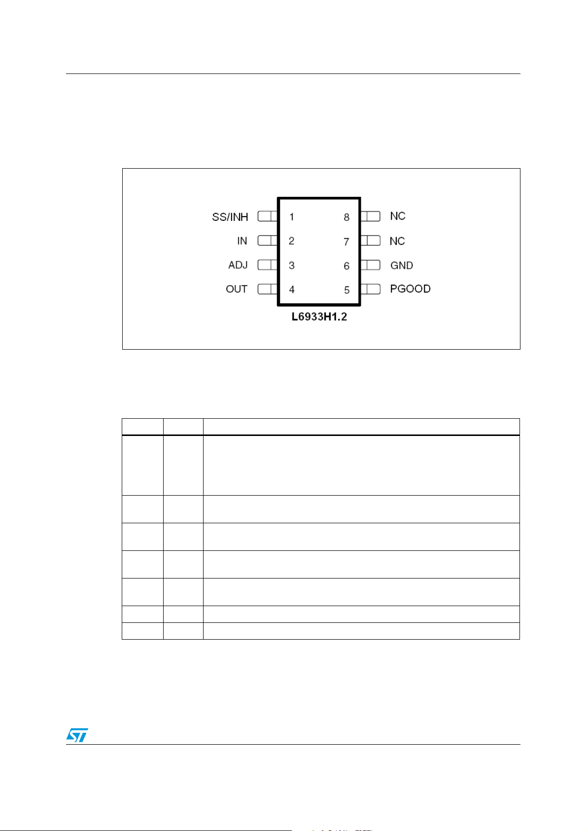
Figure 2. Pin connection (top view)
1.2 Pin description
Table 2. Pin description
Pin N° Name Description
The soft-start time is programmed connecting an external capacitor from this
pin and GND. The internal current generator forces a current of 5 µA through
SS/INH 1
VIN 2
ADJ 3
VOUT 4
PGOOD 5
NC 7, 8 Not connected
GND 6 Ground pins internally connected
the capacitor. In steady state regulation, the voltage at this pin will be about 8 V.
This pin is also used to inhibit the device: when the voltage at this pin is lower
than the 0.5 V, the device is disabled.
Supply voltage. This pin is connected to the drain of the internal N-mos.
Connect this pin to a capacitor larger than 10 µF.
Connecting this pin to a voltage divider it is possible to program the output
voltage between 1.2 V and 5 V.
Regulated output voltage. This pin is connected to the source of the internal Nmos. Connect this pin to a capacitor of 10 µF.
Power good output. The pin is open drain and detects the output voltage. It is
forced low if the output voltage is lower than 90 % the programmed voltage.
3/12

Maximum ratings L6933H1.2
2 Maximum ratings
2.1 Absolute maximum ratings
Table 3. Absolute maximum ratings
Symbol Parameter Value Unit
V
IN
2.2 Thermal data
Table 4. Thermal data
Symbol Parameter Value Unit
R
thJA
T
MAX
T
STG
1. Package mounted on board
VIN and PGood 14.5 V
SS/INH, OUT and ADJ -0.3 to (Vin +0.3) V
Maximum thermal resistance junction-ambient
Maximum junction temperature 150 °C
Storage temperature range -65 to 150 °C
34
(1)
°C/W
3 Block diagram
Figure 3. Block diagram
4/12
 Loading...