

L6925D
Fi
HIGH EFFICIENCY MONOLITHIC SYNCHRONOUS
STEP DOWN REGULATOR
1FEATURES
■ 2.7V TO 5.5V BATTERY INPUT RANGE
■ HIGH EFFICIENCY: UP TO 95%
■ INTERNAL SYNCHRONOUS SWITCH
■ NO EXTERNAL SCHOTTKY REQUIRED
■ EXTREMELY LOW QUIESCENT CURRENT
■ 800mA MAX OUTPUT CURRENT
■
ADJUSTABL E OUTPUT VOLTAGE FRO M 0.6V
■ LOW DROP-OUT OPERATION: UP TO100%
DUTY CYCLE
■ SELECTABLE LOW NOISE/LOW
CONSUMPTION MODE AT LIGHT LOAD
■ LOW BATTERY INPUT
■ LOW BATTERY OUTPUT
■ ±1% OUTPUT VOLTAGE ACCURACY
■ CURRENT-MODE CONTROL
■ 600kHz SWITCHING FREQUENCY
■ EXTERNALLY SYNCHRONIZABLE FROM
500kHz TO 1.4MHz
■ OVP
■ SHORT CIRCUIT PROTECTION
1.1 APPLICATIONS
■ BATTERY-POWERED EQUIPMENTS
■ PORTABLE INSTRUMENTS
■ CELLULAR PHONES
■ PDAs AND HAND HELD TERMINALS
■ DSC
■ GPS
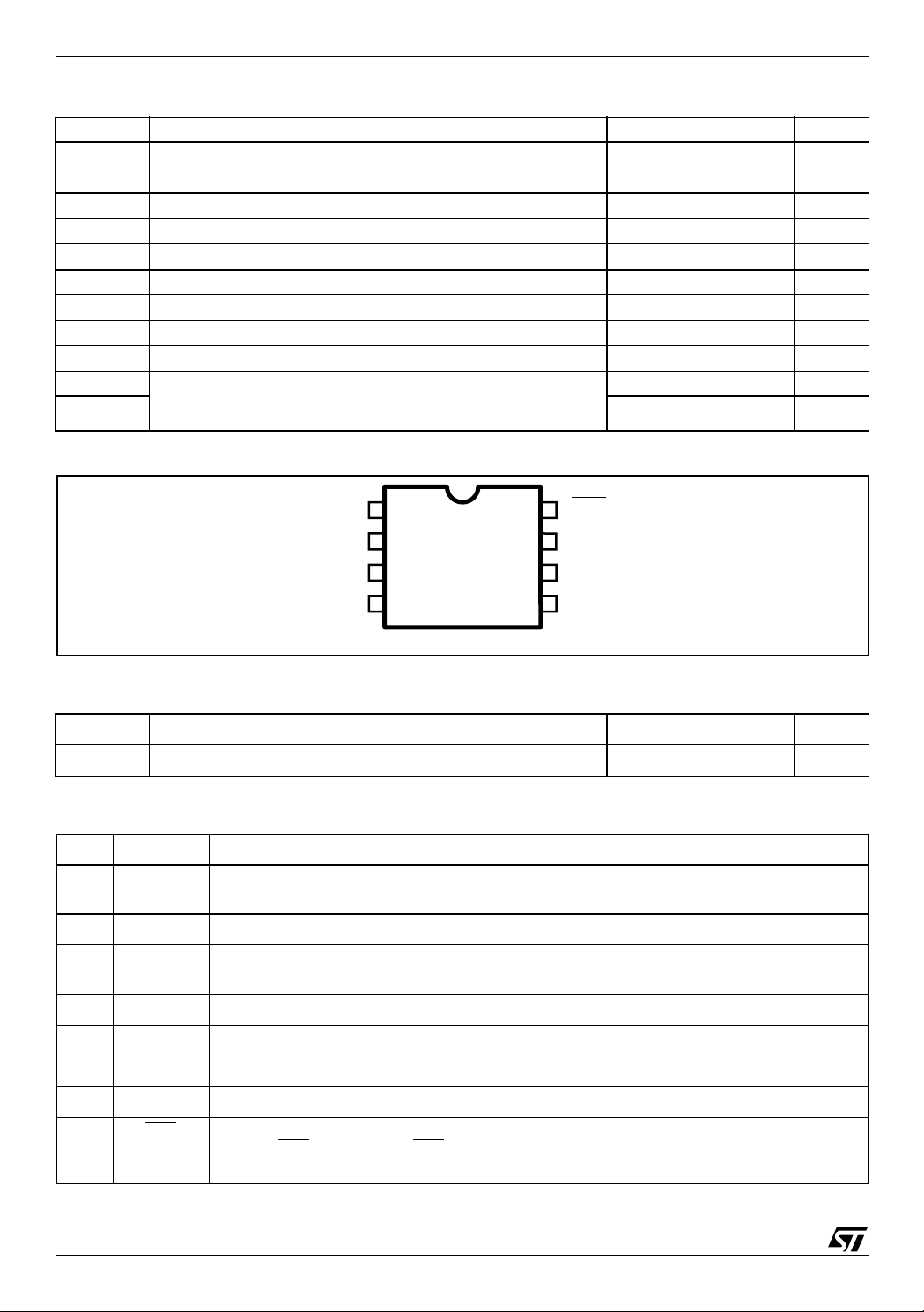
gure 1. Package
MSOP8
Table 1. Orde r Codes
Part Number Package
L6925D MSOP8 (Tube)
L6925D013TR Tape & Reel
2DESCRIPTION
The device is dc-dc monolithic regulator specifically
designed to provide extremely high efficiency.
The device has on UVLO set at 2.7V cause it is particurarly thought for single Li-ion cell applications.
Output voltage can be selected by an exter nal divider
down to 0.6V. Duty Cycle can saturate to 100% allowing low drop-out operation.
The device is based on a 600kHz fixed-frequency,
current mode-architecture. Low Consumption Mode
operation can be selected at light load conditions, allowing switching losses to be reduced. L6925D is externally synchronizable with a clock which makes it
useful in noise-sensitive applications.
LBI pin can be used to have a LBO
Battery voltage is lower than a preset value. Other
features like, Overvoltage protection, Shortcircuit
protection and Thermal Shutdown (150°C) are also
present.
signal when the
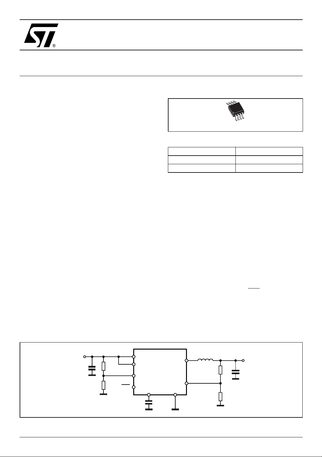
Figure 2. Applica t i on Test Circuit
V
=2.7V to 5.5V
IN
C1
10µF
6.3V
September 2004
R2
600K
R1
100K
D01IN1238B
SYNC
7
V
CC
6
LBI
1
8
LBO
24
COMP GND
220pF
C2
L 6.8µH
5
LX
VFB
3
R4
200K
R3
100K
V
=1.8V
OUT
C4
10µF
6.3V
Rev. 3
1/6
L6925D
Table 2. Absolute Maximum Ratings
Symbol Parameter Value Unit
V
V
V
1, V8
V
V
V
P
tot
T
T
stg
LX Pin Maximum Withstanding Voltage Range Test Condition: CDF-
Other pins ±2000 V
Figure 3. Pin Connection
Input voltage -0.3 to 6 V
6
Output switching voltage -1 to V
5
Low Battery Input, Low Battery Output -0.3 to V
Feedback voltage -0.3 to V
3
Error Amplifier Output Voltage -0.3 to V
2
Syncronization / Mode Selector -0.3 to V
7
CC
CC
CC
CC
CC
Power dissipation at Tamb=70°C0.45W
Junction operating temperature range -40 to 150 °C
j
Storage temperature range -65 to 150 °C
±1000 V
AEC-Q100-002- “Human Body Model” Acceptance Criteria:
“Normal Performance’
V
V
V
V
V
LBI
COMP
VFB
GND
1
2
3
4LX
D01IN1239A/mod
7
6
5
LBO8
SYNC
V
CC
Table 3. Thermal Data
Symbol Parameter Value Unit
R
th j-amb
Thermal Resistance Junction to Ambient 180 °C/W
Table 4. Pin Functions
N Name Description
1 LBI Battery low voltage detector input. The internal threshold is set to 0.6V. The external threshold
can be adjusted by using an external resistor divider.
2 COMP Error amplifier output. Compensate it with a 220pF capacitor
3 VFB Error amplifier input. The output voltage can be adjusted by using an external resistor divider
connected to this pin (V
4 GND Ground.
= 0.6V).
FB
5 LX Switch node connection to the inductor.
6 VCC Input voltage.
7 SYNC This pin allows to select Low Noise/ Low Consumption Mode or to sychronize the device.
8LBO
Battery low voltage detector output. If the voltage at the LBI pin drops below the internal
thrshold, LBO
goes low. The LBO is an open drain output. A pull_up resistor should be
connected between the pin and the output voltage
2/6

L6925D
Table 5. ELECTRICAL CHARACTERISTICS (TJ = 25°C, VCC = 3.6V unless otherwise specified)
Symbol Parameter Test Condition Min Typ Max Unit
V
cc
V
cc ON
V
cc OFF
V
cc hys
R
p
R
n
I
lim
V
out
f
osc
f
sync
DC CHARACTERISTICS
I
q
Operating input voltage After Turn On 2.7 5.5 V
Turn On threshold 2.8 V
Turn Off threshold 2.65 V
Hysteresis 150 mV
High side Ron V
Low side Ron V
= 3.6V, I
cc
= 3.6V, I
cc
=100mA 240 mΩ
lx
=100mA 215 mΩ
lx
Peak current limit Vcc = 3.6V 1.2 A
Valley current limit V
= 3.6V 1.4 A
cc
Output voltage range 0.6 Vcc V
Oscillator frequency 600 KHz
Sync mode clock (*) 500 1400 KHz
Quiescent current
(low noise mode)
Quiescent current
(low cunsumption mode)
V
= 0V, no load,
sync
V
> 0.6V
FB
V
= Vcc, no load,
sync
VFB > 0.6V
230 µA
25 µA
I
sh
I
lx
Shutdown current V
< 2.7V, VFB > 0.6V 0.2 µA
cc
LX leakage current (*) Vcc < 2.7V, V
V
< 2.7V, V
cc
= V
LX
cc
= 0V 1 µA
LX
1 µA
ERROR AMPLIFIER CHARACTERISTICS
V
fb
I
fb
Voltage feedback 0.593 0.6 0.607 V
Feedback input current (*) VFB = 0.6V 25 nA
SYNC/MODE FUNCTION
V
sync_H
V
sync_L
Sync mode threshold high 1.3 V
Sync mode threshold low 0.5 V
LB SECTION
V
LBI
V
LBO
I
LK-LBO
LBI Threshold 0.6 V
LBO Logic Low I
LBO Leakage Current (*)
= 1mA, Vcc = 3.6V,
sink
V
< 0.6V
LBI
V
V
LBO
LBI
= 3.6V,
> 0.6V
Vcc = 3.6V
0.2 0.4 V
,
50 nA
PROTECTIONS
HOVP Hard overvoltage threshold 10 %Vout
(*) Guarant eed by design
3/6

L6925D
Figure 4. MSOP8 Mechanical Data & Package Dimensions
DIM.
A 1.10 0.043
A1 0.050 0.150 0.002 0.006
A2 0.750 0.850 0.950 0.03 0.033 0.037
b 0.250 0.400 0.010 0.016
c 0.130 0.230 0.005 0.009
D (1) 2.900 3.000 3.100 0.114 0.118 0.122
E 4.650 4.900 5.150 0.183 0.193 0.20
E1 (1) 2.900 3.000 3.100 0.114 0.118 0.122
e 0.650 0.026
L 0.400 0.550 0.700 0.016 0.022 0.028
L1 0.950 0.037
k 0˚ (min.) 6˚ (max.)
aaa 0.100 0.004
Note: 1. D and F doe s not include mold flash o r protru sions.
mm inch
MIN. TYP. MAX. MIN. TYP. MAX.
Mold flash or potrusions shall not exceed 0.15mm
(.006inch) per side.
OUTLINE AND
MECHANICAL DA T A
MSOP8
(Bod y 3mm)
4/6

Table 6. Revision History
Date Revision Description of Changes
January 2004 2 First Issue in EDOCS DMS
September 2004 3 Changed Style-sheet and Table 2
L6925D
5/6

L6925D
Information furnished is believed to be accurate and reliable. However, STMicroelectronics assumes no responsibility for the consequences
of use of such information nor for any infringement of patents or other rights of third parties which may result from its use. No license is granted
by implic ation or otherwise under any patent or p at ent rights of STMicroelectronics. Spec i fications mentioned i n this publication are subject
to change without notice. This publication supersedes and replaces all information previously supplied. STMicroelectronics products are not
authorized for use as cri tical comp onents in life support dev i ces or systems wi thout express written approval of STMicroel ectronics.
The ST logo is a registered trademark of STMic roelectronic s.
All other nam es are the property of th ei r respectiv e owners
© 2004 STMi croelectro ni cs - All rights reserved
Australi a - Belgium - Brazil - Canada - China - Czech Rep ubl i c - Finland - France - Germ any - Hong Kong - India - Is rael - Italy - Japan -
Malaysia - M al ta - Morocco - S i ngapore - Sp ai n - Sweden - Sw i t zerland - Un i ted Kingdom - United States of Ameri ca
STMicroelectronic s group of com panies
www.st.com
6/6
 Loading...